

Introduction to PIC18F4520
- PIC18F4520 is a PIC microcontroller, introduced Microchip, and mainly used in automation and embedded systems. It comes in three packages known as PDIP, QFN, and TQFP where the first one is 40-pin (mostly used) while other two come with a 44-pin interface.
- This microcontroller version comes with CPU, timers, 10-Bit ADC and other peripherals that are mainly used to develop a connection with external devices.
- This PIC version, like other models in the PIC community, contains everything that is required to make an embedded system and drive automation.
- The PIC18F4520 contains 256 bytes of EEPROM data memory, 1536 bytes of RAM, and program memory of 32K.
- It also incorporates 2 Comparators,10-bit Analog-to-Digital (A/D) converter with 13 channels, and houses decent memory endurance around 1,000,000 for EEPROM and 100,000 for program memory.
- The Enhanced Universal Asynchronous Receiver Transmitter (EUSART) feature is useful for developing the serial communication with other devices.
- The asynchronous serial port is added on the chip that can be interfaced both ways i.e. 3-wire Serial Peripheral Interface (SPI™) or the 2-wire Inter-Integrated Circuit (I²C™) Bus.
- Wide operating voltage range (2.0V-5.5V)
- Multiplexed Master Clear with pull-up/input pin
- In-Circuit Serial Programming™ (ICSP™) via two pins
- Power-Saving Sleep mode
- C compiler optimized architecture
- Industrial and Extended Temperature range
- Power-up Timer (PWRT) and Oscillator Start-up Timer (OST)
- Power-on Reset (POR)
- In-Circuit Debug (ICD) via two pins
- Brown-out Reset (BOR) with software control option
- Watchdog Timer (WDT)
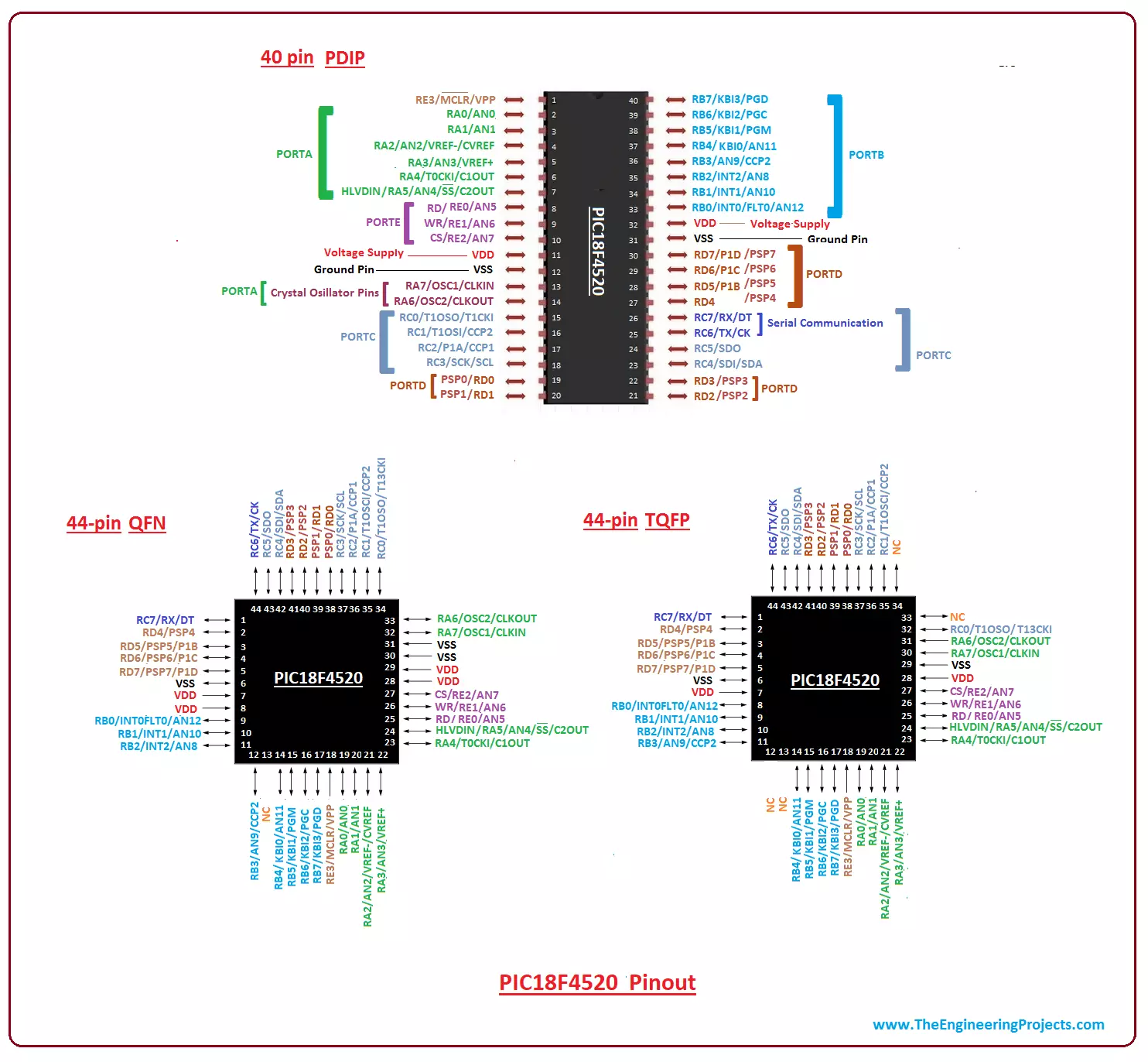
1. PIC18F4520 Pinout and Description
You have got a clear idea about this PIC18F4520 model. In this section, we jot down the pinout of the controller and cover a detailed description of each pin.PIC18F4520 Pinout
Following figure shows the pinout of PIC18F4520.- The PDIP module comes with 40-pin interface while other two QFN and TQFP contain 44-pin on each module.
- The former module is mainly used for developing individual projects while the other two are incorporated in industrial electronic devices.
Pin Description
Every pin on the module comes with a unique function, used as per the requirement of the project. And some pins incorporate multiple functions. The following figure shows the complete pinout description of this tiny PIC module.| Pin# | Pin Name | Pin Description |
|---|---|---|
| 2 | RA0/AN0 RA0 AN0 | Digital I/O Pin Analog Input 0 Pin |
| 3 | RA1/AN1 RA1 AN1 | Digital I/O Pin Analog Input 1 Pin |
| 4 | RA2/AN/VREF- RA2 AN2 VREF- | Digital I/O Pin Analog Input 2 Pin ADC Reference Input Voltage (low) |
| 5 | RA3/AN/VREF+ RA3 AN3 VREF+ | Digital I/O Pin Analog Input 3 Pin ADC Reference Input Voltage (high) |
| 6 | RA4/T0CKI/C1OUT RA4 T0CKI C1OUT | Digital I/O Pin External clock input for Timer0 Output Comparator 1 |
| 7 | RA5/AN4/SS/HLVDIN/C2OUT RA5 AN4 SS HLVDIN C2OUT | Digital I/O Pin Analog Input 4 Pin Slave Select input for SPI (High, Low) Detect Input for Low Voltage Output Comparator 2 |
| 33 | RB0/INT0/FLT0/AN12 RB0 INT0 FLT0 AN12 | PORTB can be programmed with software Digital I/O Pin External Interrupt 0 Fault Input for Enhanced CCP1 Analog Input |
| 34 | RB1/INT1/AN10 RB1 INT1 AN10 | Digital I/O Pin External Interrupt 1 Analog input 10 |
| 35 | RB2/INT2/AN8 RB2 INT2 AN8 | Digital I/O Pin External Interrupt 2 Analog input 8 |
| 36 | RB3/CCP2 RB3 AN9 CCP2 | Digital I/O Pin Analog input 9 Output for Compare2 and PWM2, and Input for Capture2 |
| 37 | RB4/KBI0/AN11 RB4 KBI0 AN11 | Digital I/O Pin Interrupt-on-change pin Analog input 11 |
| 38 | RB5/KBI1/PGM RB5 KBI1 PGM | Digital I/O Pin Interrupt-on-change pin ICSP programming enable pin for low voltage |
| 39 | RB6/KBI2/PGC RB6 KBI2 PGC | Digital I/O Pin Interrupt-on-change pin ICSP programming clock and In-Circuit Debugger pin |
| 40 | RB7/KBI3/PGD RB7 KBI3 PGD | Digital I/O Pin Interrupt-on-change pin ICSP programming data and In-Circuit Debugger pin |
| 15 | RC0/T1OSO/T13CKI RC0 T1OSO T13CKI | Digital I/O Pin Oscillator output for Timer1 External clock input for Timer1/Timer3 |
| 16 | RC1/T1OSI/CCP2 RC1 T1OSI CCP2 | Digital I/O Pin Oscillator input for Timer1 Output for Compare2 and PWM2, Input for Capture2 |
| 17 | RC2/CCP1/P1A RC2 CCP1 P1A | Digital I/O Pin Output for Compare1 and PWM1, Input for Capture1 Enhanced CCP1 Output |
| 18 | RC3/SCK/SCL RC3 SCK SCL | Digital I/O Pin SPI Module Synchronous serial clock input/output I2C Module Synchronous serial clock input/output |
| 23 | RC4/SDI/SDA RC4 SDI SDA | Digital I/O Pin SPI Data-In Pin I2C Data I/O Pin |
| 24 | RC5/SDO RC5 SDO | Digital I/O Pin SPI Data-Out Pin |
| 25 | RC6/TX/CK RC6 TX CK | Digital I/O Pin Asynchronous Transmit (USART) Synchronous Clock (USART) |
| 26 | RC7/RX/DT RC7 RX DT | Digital I/O Pin Asynchronous Receive (USART) Synchronous Data (USART) |
| 19 | RD0/PSP0 | Digital I/O Pin Parallel Slave Port (PSP) for D0 with TTL input buffers |
| 20 | RD1/PSP1 | Digital I/O Pin Parallel Slave Port for D1 with TTL input buffers |
| 21 | RD2/PSP2 | Digital I/O Pin Parallel Slave Port for D2 with TTL input buffers |
| 22 | RD3/PSP3 | Digital I/O Pin Parallel Slave Port for D3 with TTL input buffers |
| 27 | RD4/PSP4 | Digital I/O Pin Parallel Slave Port for D4 with TTL input buffers |
| 28 | RD5/PSP5 | Digital I/O Pin Parallel Slave Port for D5 with TTL input buffers |
| 29 | RD6/PSP6 | Digital I/O Pin Parallel Slave Port for D6 with TTL input buffers |
| 30 | RD7/PSP7 | Digital I/O Pin Parallel Slave Port for D7 with TTL input buffers |
| 8 | RE0/RD/AN5 RE0 RD AN5 | Digital I/O Pin PSP Read Control Analog input 5 Pin |
| 9 | RE1/WR/AN6 RE1 WR AN6 | Digital I/O Pin PSP Write Control Analog input 6 Pin |
| 10 | RE2/CS/AN7 RE2 CS AN7 | Digital I/O Pin PSP Chip Select Control Analog input 7 Pin |
| 1 | MCLR/VPP MCLR VPP | ICSP Programming Enable Pin Master Clear Active Low Reset Pin |
| 13 | OSC1/CLKI OSC1 CLKI | Crystal Oscillator Input Pin |
| 14 | OSC2/CLKO/RA6 OSC2 CLKO RA6 | Crystal Oscillator Output Pin |
| 12,31 | VSS | Ground pin |
| 11,32 | VDD | Voltage pin |
- This table will help you understand the function associated with each pin.
2. PIC18F4520 Features
Features are very important for any device that makes it unique from its counterparts. The following figure shows the complete features of PIC18F4520.| PIC18F4520 Features | |
|---|---|
| No. of Pins | 40 |
| CPU | 8-Bit PIC |
| Operating Voltage | 2 to 5.5 V |
| Program Memory | 32K |
| Program Memory (Instructions) | 16384 |
| RAM | 1536 Bytes |
| EEPROM | 256 Bytes |
| ADC Number of Channels | 10-Bit 13 |
| I/O Ports (5) I/O Pins | A,B,C,D,E 36 |
| Packages | 40-pin PDIP 44-pin QFN 44-pin TQFP |
| External Oscillator | up to 40 MHz |
| Timer (4) | 16-Bit Timer (3) 8-Bit Timer (1) |
| USART Protocol | 1 |
| I2C Protocol | Yes |
| SPI Protocol | Yes |
| Brown-out Reset | Yes |
| Watchdog Timer | Yes |
| Comparators | 2 |
| Master Synchronous Serial Port (MSSP) module | 1 |
| Capture/Compare/PWM | 16bit/16bit/10bit |
| Power Saving Sleep Mode | Yes |
| Selectable Oscillator Option | Yes |
| Operating High-current sink/source Each pin | 25mA |
| Programmable High/Low-Voltage Detect | -Yes |
| Oscillator Start-up Timer | Yes |
- These features help you identify the main characteristics of the controller that are appropriate for designing and developing for the certain project.
3. PIC18F4520 Functions
This PIC model is capable of performing many functions similar to other controllers in the PIC community. Following are the main functions of PIC18F4520.Timer
PIC18F4520 comes with three 16-bit and one 8-bit timer that can be used as a timer as well as a counter. All three timers contain internal and external clock select capability. The timer mode mainly increments the instruction cycle while the counter mode is used to increment the rising and falling edge of the pin.Brown Out Reset (BOR)
The BOR is a very useful function that allows this controller to reset once the Vdd (voltage supply) drops below a brownout threshold voltage. The multiple voltage ranges are used and provided to protect the chip once the power drops at the voltage supply line. The Power Up Timer must be kept enabled, in order to put the delay in returning the device from a BOR function, t The BOR mode can be configured both ways i.e. through BOREN settings in a register as well through programming.In-Circuit Serial Programming
In-circuit serial programming (ICSP), also called In-system programming (ISP), is a feature added to this device that makes it enable to be programmed in the required system after installation, setting it free from programming the device before making it compatible with the certain project.USART
This controller version comes with USART module, that stands for Universal Synchronous and Asynchronous Receiver and Transmitter, and is mainly used for setting up the serial communication with external devices. There are two parts of this module called TX and RX where former is known as transmitting component that is used for transmitting serial data while later is known as receiving component, used for receiving the serial data across the attached devices.Watchdog Timer
PIC18F4520 contains a built-in watchdog timer that brings the controller in reset position if the program hangs up during compilation or gets stuck in the infinite loop. It is worth mentioning here, this timer must be reset to the initial value after every 3 instructions in order to avoid it going to zero value in normal conditions. The watchdog timer is more or less a countdown timer that starts from 1000 and ultimately goes down to zero.Power On Reset
Power On Reset function is very helpful and resets the controller and starts it from scratch when Vdd raises above a certain threshold value. This function is very useful to prevent the device from malfunctioning.Power Managed Modes
PIC18F4520 provides total 7 operating modes that help in more efficient power management. These modes offer multiple options for selective power conservation in a variety of applications. The power managed modes are mainly divided into three main categories called:- Run modes
- Sleep mode
- Idle modes
Master Clear Reset (MCLR)
The MCLR pin is used for calling the external reset for the chip. The reset is triggered by keeping this pin at a LOW value and is not dependent on the internal resets. The noise filter is added in the MCLR executing process that helps in detecting and removing the small pulses. The MCLRE configuration bit can also be used to disable MCLR input.4. PIC Compiler
- Microchip comes with its own standard compiler for the PIC controller called MPLAB C18 Compiler. You can get this compiler online from the Official Microchip Site.
- MikroC Pro For PIC is a third party software mainly used as a replacement of Microchip standard compiler.
- These Top 3 PIC C Compilers give you many options to choose from to pick any compiler as per your needs and demands.
- The code written in the compiler generates a hex file which is then uploaded to the microcontroller to execute the number of instructions.
- The PICKit3 is a standard PIC burner, mainly used for burning the code in the controller. There are other burners also available in the market but PICKit3 is mostly used and preferred for the PIC controllers.
5. PIC18F4520 Memory Layout and Working
The memory of the module is very useful for storing a number of instruction which can be divided into three major types: Program Memory Data EEPROM Data RAM Let's discuss each memory one by one and highlight the main functions associated with them.Program Memory
The Program memory, also known as ROM memory or Non-Volatile memory, stores the running program permanently. It doesn't depend on the power supply i.e. stores the program in the absence of the main power supply. The ROM memory is about 32K and is made with FLASH Technology.Data EEPROM
This memory is similar to ROM memory in one way or the other and stores running program permanently with one limitation i.e. the instructions in EEPROM can be controlled and modified during the controller operation. The EEPROM comes with memory space around 256 bytes and can be accessed and addressed by multiple control registers.Data RAM
RAM memory, also known as volatile memory, stores the program temporarily and removes the stored program once the power supply is removed. It is classified into two main parts called General-purpose registers (GPR) Special-function registers (SFR) This memory is volatile in nature as it stores the program temporarily and is power dependent i.e. once the power supply is turned off the instructions stored in the RAM will be removed. The RAM memory registers are the data holding places that can hold instruction, storage address, and any kind of data ranging from an individual character to bit sequence. The data memory can be employed as static RAM where each register comes with a 12-bit address. This memory is comprised of a total 16 banks and each bank contains a memory space of around 256 bytes.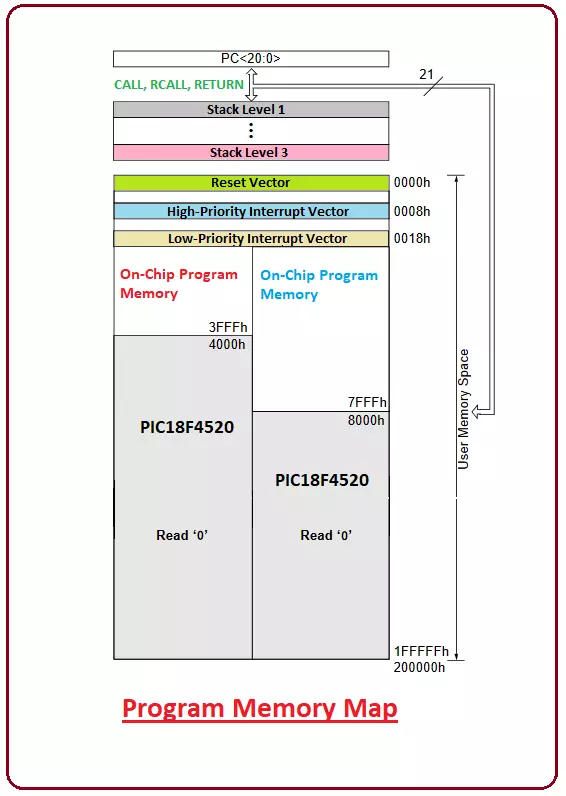
6. PIC18F4520 Block Diagram
You have got a brief overview of pinout, its description and main features of the controller. In this section, we discuss the main block diagram of the microcontroller so you can get an idea how each function in the controller is related and connected to each other.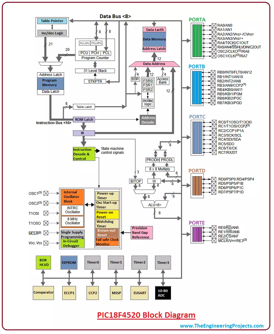
- PIC18F4520 comes with five ports where each port contains 8 pins except the E port that comes with 4 pins which also include MCLR (master clear pin).
- This device can be configured using 10 different oscillator modes where different capacitor values are required to generate acceptable oscillator operation. The user must test oscillator performance with the suitable VDD and temperature range for the required project.
7. PIC18F4520 Projects and Applications
- PIC18F4520 is widely used in home and industrial automation
- Student projects for motor controlling and sensor interfacing
- GPS and security systems
- Gas sensor projects
- Production of temperature data logger
- Serial Communication
- Central heating projects
- Embedded system
8. Why Use PIC MicroControllers
- PIC microcontrollers are widely used in multiple applications as they come with user-friendly interface and easy onboard architecture that requires little or no prior skills before getting familiar with the chip.
- They can perform a number of functions using minimum circuitry and are cheap in price as compared to other modules available in the market.
- Minimum power consumption is another ability that makes this controller an ideal choice for the projects where power limitation is a major concern.
- PIC controllers stay ahead of other Atmel controller like 8051 in terms of their higher processing speed and efficiency.
