

Introduction to JFET
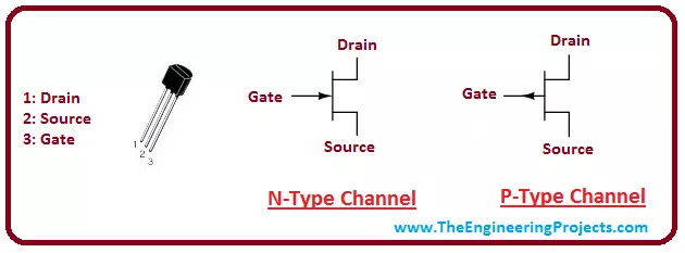
- JFET (Junction Field Effect Transistor) is a uni-polar voltage-controlled device that consists of three terminals called drain, source and gate.
- Unlike bipolar junction transistors which are bipolar current-controlled devices in which a small amount of base current is used to control a large amount of current at the collector and emitter side, JFET is a uni-polar voltage-controlled device in which voltage applied to the gate terminal allows the current to flow through JFET, resulting in input applied voltage equals to the current flowing through the transistor.
- In JFET, gate is always negatively biased as compared to source.
- As compared to bipolar junction transistors, JFET are uni-polar because current carriers in case of JFET are either electrons or holes while bipolar junction transistors are operated by the movement of both electrons and holes.
- The operation of JFET depends on the electric field created by input applied voltage, hence it is called Field Effect Transistor.
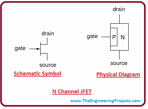
- JFET can be classified into two types on the bases of their operation i.e. N-Type and P-Type JFET.
- In JFET, current carrying path between drain and source is called channel which contains no pn-junction. Channel can be made up of P-Type or N-Type semiconductor.
- Current flowing through this channel widely depends on the input voltage applied to the gate terminal of JFET.
- Field effect transistors generally comes in two types JFET (Junction Field Effect Transistors) and MOSFET( Metal Oxide Semiconductor Field Effect Transistors)
- As stated earlier, JFET contains no pn-junction, instead it comes with channel that consists of N type or P type semiconductor that passes between source and drain terminals of JFET.
- N-Type Configuration
- P-Type Configuration
1: N-Type Configuration
- In N-Type configuration current flowing through the channel is negative i.e. current flow is carried out by the flow of electrons which are also termed as donor impurities.
- The measure of conductivity of electron in N-Type configuration is much higher than the holes in P-Type configuration, because electrons come with high level of mobility than holes. Hence, in terms of conductivity, N-Type configuration is more efficient than P-Type configuration.
- Channel is a conducting path between drain and source. Within this channel, there lies a third terminal called Gate at which input voltage is applied that is used to control the current flowing through the JFET.
- As channel is resistive in nature, resulting in creating the voltage gradient which becomes less positive as we move from drain to source terminal. This less positive voltage makes drain terminal high reverse biased and source terminal low reverse biased. This bias creates a depletion region whose width is directly proportional to the bias itself.
- The current carrying path between source and drain is controlled by the voltage applied to the gate terminal. In an N-Type configuration of JFET this gate voltage is negative while in case of P-Type configuration it is positive.
- It is important to note that gate current in reverse biased condition in the JEFT is practically zero, while base current in Bipolar junction transistor always comes with a value greater than zero.
N-Type Channel Biasing
- Following is the figure shows N-Type semiconductor with P-Type material which forms the reverse biased PN-junction that creates a depletion region around the gate terminal of JFET.
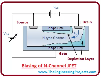
- Depletion region will be created in the absence of external voltages. JFET are also termed as depletion mode components.
- The depletion region will create a voltage gradient of some thickness which ultimately limits the flow of current, hence results in increasing the overall resistance of FET.
- It is clear from the figure above that most part of depletion region lies between the gate and drain terminals which least part lies between the gate and source terminals which means resistance between gate and drain terminal appears more than the resistance between gate and source terminals.
- In the absence of external input voltage at gate and small voltage at the drain and source Vds allows the saturation current to flow between drain and source.
- The amount of current flowing through the pn-junction will be restricted by the depletion region around the pn-junction.
- It is important to note, if we apply negative voltage at the gate and source Vgs terminals, it will cause the depletion region to grow which ultimately restricts the flow of current, hence results in decreasing the overall conduction of transistor.
- If the voltage applied at the gate terminal Vgs appears to be more negative, it will allow the depletion region to increase and results in decreasing the overall width of channel. The moment comes when applied voltage at gate terminal appears to be negative to the point that will squeeze the channel and won't allow a fraction of current to flow between source and drain terminals.
- The negative voltage applied to the gate terminal at which no current flows between drain and source terminals is called "Pinch-off Voltage".
- In pinch off region negative voltage at the gate terminal Vgs controls the overall conductivity of the channel. This is the reason JFET are called voltage controlled devices.
- Voltage appears at the gate terminal must not be positive, otherwise it will make resistance zero and allows the current to flow between gate terminal instead of source terminal. Positive voltage at the base terminal can damage the transistor at large.
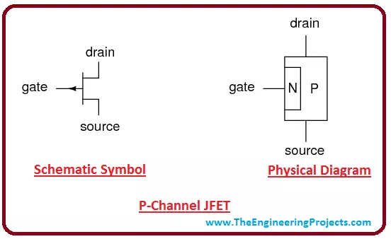
2: P-Type Configuration:
- In P-Type configuration current flowing through the channel is positive i.e. current flow is carried out by the flow of holes which are also termed as acceptor impurities. Both N-Type and P-Type configurations come with same characteristics with some exceptions.
- Current carriers in N-Type configuration are electorn, hence current appears to be negative
- Current carriers in P-Type configuration are holes, hence current appears to be positive.
- Biasing voltage in P-Type configuration comes with reverse polarity.
- The voltage applied at the gate terminal is used to control the current flowing between source and drain. As JFET is a voltage controlled device and no current flows through gate terminals Ig=0. Hence in that case, current flowing out from source terminal will be equal to the current flowing into the drain terminal i.e. Is=Id
V * I Curves of N-Channel JFET
Following figure depicts the four region of operation of JFET.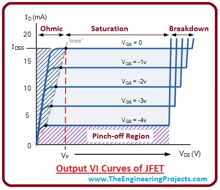
- Ohmic Region: Region is called ohmic region when Vgs=0. In this region JFET operates like a voltage controlled resistor.
- Pinch off or Cut-off Region: It is region at which voltage applied to the gate is negative to the point which causes depletion region to increase and allows the current carrying width to decrease till it disappears, resulting in maximum resistance to appear and current flowing through the channel will be zero.
- Active or Saturation Region: The region that is controlled by gate voltage Vgs and where JFET becomes good conductor is called active region. Vds has no effect on active region.
- Breakdown Region: Region is termed as breakdown region where voltage between source and drain appears to be maximum to the point where it breaks the resistive channel and allows the current to flow between the channel.
V * I Curves for P-Type JFET
- The curves for P-Type configuration appear to be same with one exception i.e. Increase in positive voltage at the gate terminal will decrease the current at the Drain terminal Id.
Formula for Drain Current and Drain-Source Channel Resistance
- Drain current at the saturation region can be calculated as follows:
Id= Idss * [ 1 - Vgs / Vp ]
- Id lies between zero to Idss.
- Similarly, if we know drain source voltage Vds and drain current Id, we can calculate the drain-source channel resistance.
Rds = ?Vds / ? I d = 1 / gm
- Here gm represents the "transconductance gain"
Different Modes of Operation of FETs:
FETs can be classified into three different modes of configuration.- Common Source Configuration
- Common Gate Configuration
- Common Drain Configuration
1: Common Source Configuration CS:
Common source configuration is an analogous to the common emitter configuration in the bipolar junction transistors. In this configuration input voltage is applied to the gate terminal and output we get is from the drain terminal. This mode of operation comes with amplified voltage and high impedance, hence it is mostly used in high audio frequency amplifies. As this is an amplifying circuit, it allows the output to be diverted 180º from its input.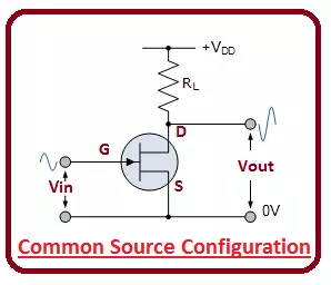
2: Common Gate Configuration CG:
Common gate configuration is an analogous to the common base configuration in the bipolar junction transistors. In this configuration input voltage is applied to the source terminal and output appears at the drain terminal while gate is connected to ground. In this configuration impedance will be low as compared to common source configuration. This configuration is mostly used in high frequency and impedance matching circuits. Unlike common source configuration, here "output signal is in phase with the input signal"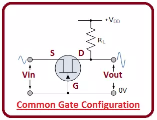
3: Common Drain Configuration CD:
Common drain configuration is an analogous to the common collector configuration in the bipolar junction transistors. In this configuration input voltage is applied to the gate and output signal is collected from the source. It is important to note there is no signal applied to the drain terminal. Vdd simply depicts the bias voltage. Similar to common gate configuration, here "output signal is in phase with the input signal"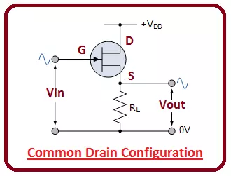
Comparison between BJT and JFET
-
- Both, bipolar junction transistors and uni-polar field effect transistors encompass same characteristics with some exceptions.
- BJT are bipolar devices i.e. they are operated by the movement of both electrons and holes. JFET are unipolar devices i.e. they are operated by the movement of either electrons or holes.
- As compared to Bipolar junction transistors, JFET comes in much smaller form and can be used in many tiny electronic chips.
- One major feature that differentiates between bipolar junction transistors and JFET is the input impedence. It is very high in case of JFET while it appears very low in bipolar junction transistors.
Applications
- JFET are widely used in many electronic appliations. They are mainly used for amplification purpose.
- JFET are used to obtain high frequency audio signal.
- They are useful for obtaining impedance matching circuits.
