

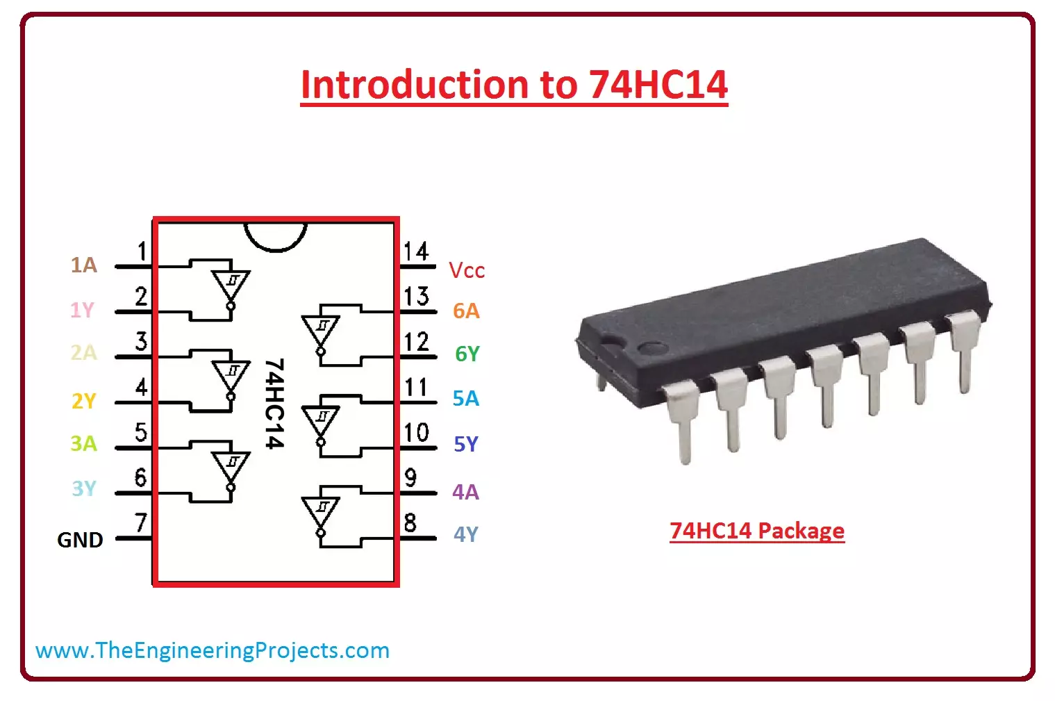
Introduction to 74HC14
- 74HC14 is a member of 74XXXX integrated circuit series, it consists of logic gates. This module is also called HEX inverting Schmitt trigger.
- It is a high-speed CMOS Schmitt Inverter which consists of C2MOS technology. It provided high-speed operation like LSTTL, by using low power.
- Its pin configurations are the same as the 74HC04D, but the inputs have 25% Vcc hysteresis.
- Due to its Schmitt trigger function, it is used as a line receiver which will receive slow input signals.
- Its all inputs are equipped with protection circuits for static discharge or fleeting voltage.

74HC14 Pinout & Description
- These are the main pinout of 74HC14, which are described below. For further information, let's discuss them one by one.
| Pin# | Type | Parameters |
| Pin#1 | 1A | It is an input of gate 1. |
| Pin#3 | 2A | It is an input of gate 2. |
| Pin#5 | 3A | It is an input of gate 3. |
| Pin#9 | 4A | It is an input of gate 4. |
| Pin#11 | 5A | -It is an input of gate 5. |
| Pin#13 | 6A | It is an input of gate 6. |
| Pin#7 | GND | It is connected to ground. |
| Pin#14 | Vcc | It is connected to a positive voltage to provide power to all six gates. |
| Pin#2 | 1Y | It is an output of gate 1 |
| Pin#4 | 2Y | It is an output of gate 2 |
| Pin#6 | 3Y | It is an output of gate 3 |
| Pin#8 | 4Y | It is an output of gate 4 |
| Pin#10 | 5Y | It is an output of gate 5 |
| Pin#12 | 6Y | It is an output of gate 6 |

Features of 74HC14
- These are the main features of 74HC14, which are described below.
- Its operating voltage is -0.5V to +7.0V.
- The maximum current allowed to daw through each gate is 25mA.
- Maximum total current can pass through Vcc or GND pins are 50mA.
- This device is lead-free.
- This module has a TTL type outputs.
- It has noise immunity.
- It maximum ESD is 2kv.
- Its typical rise time is 85-625ns (depending on supply voltage)
- Its typically fall time is 85-625ns (depending on supply voltage).
- It's working temperature is -55°C to 125 °C.
- It's working voltage range is 2.0 to 6.0 V.
- Its output drive capability is 10 LSTTL Loads.
- It has the ability to directly interface to CMOS, NMOS, and TTL.
- This module is compatible with the JEDEC standard No.7A requirements.
- Its chips consist of 60 FETs or equivalent gates.
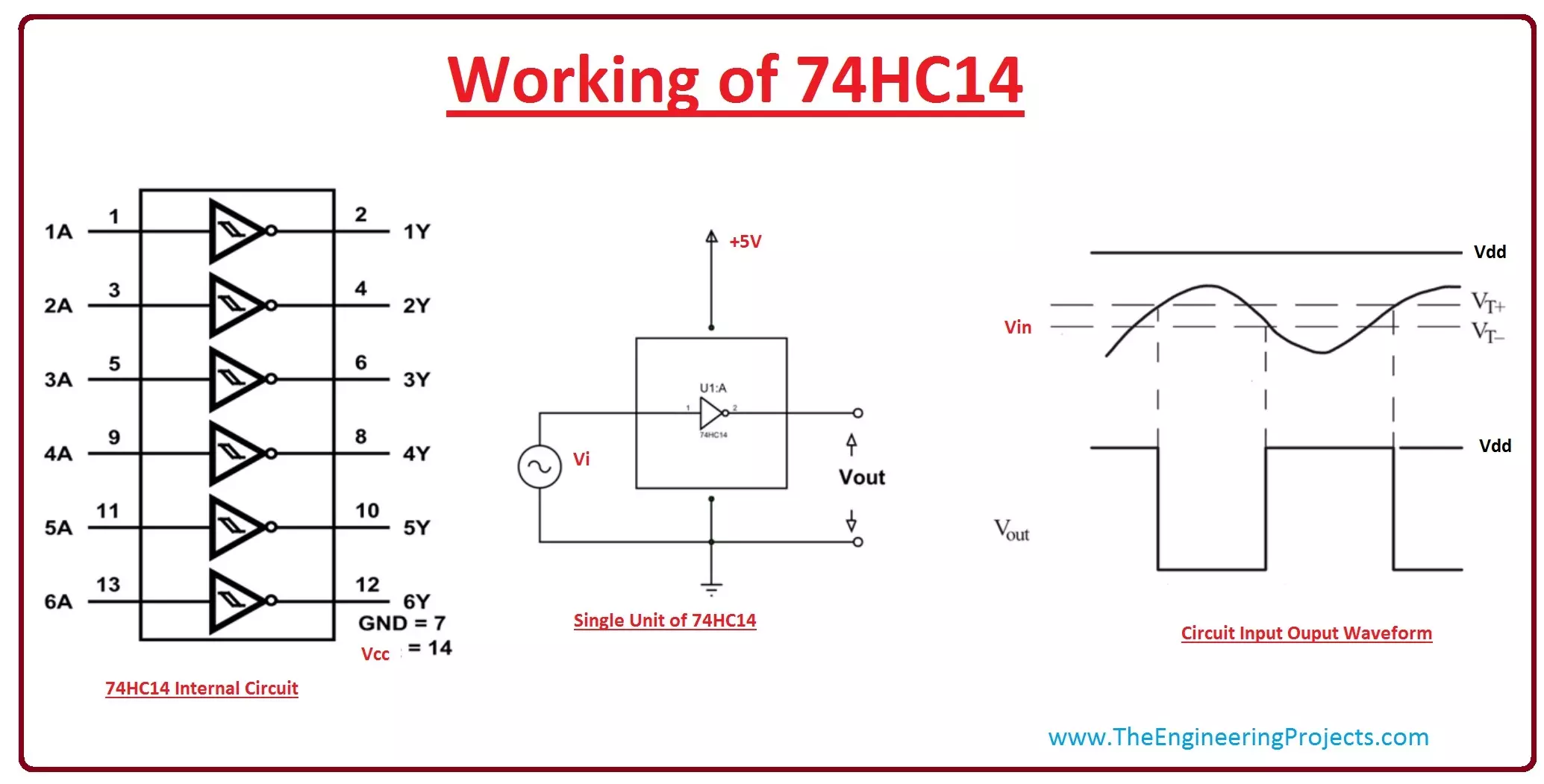
Working of 74HC14
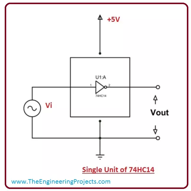
- As mentioned earlier, there are 6 Schmitt Trigger Gates (inverted) in 74HC14, and we can used each of these gates separately.
- The internal circuit of 74HC14 is shown in the given diagram.
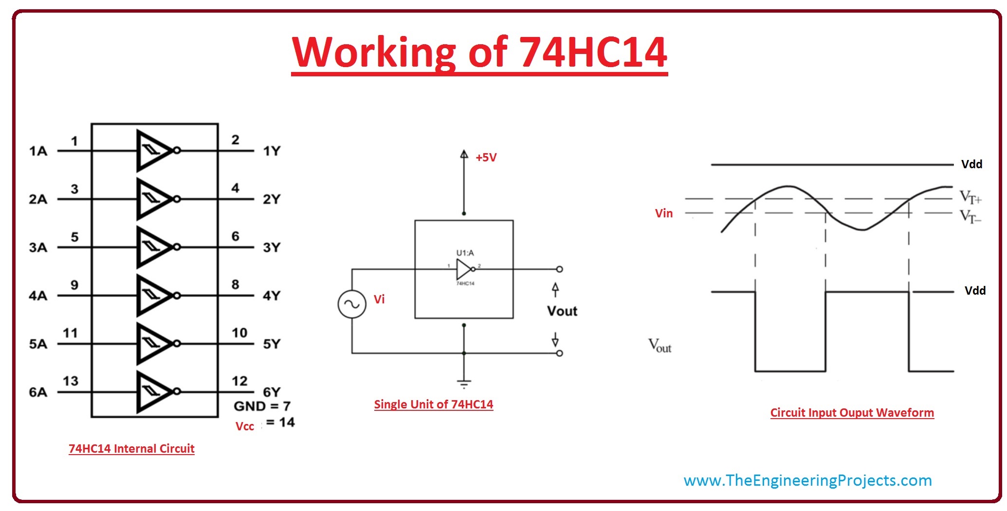
- For our knowledge how single gate works let's take one gate and connect it with power supply and analog signal at the input.
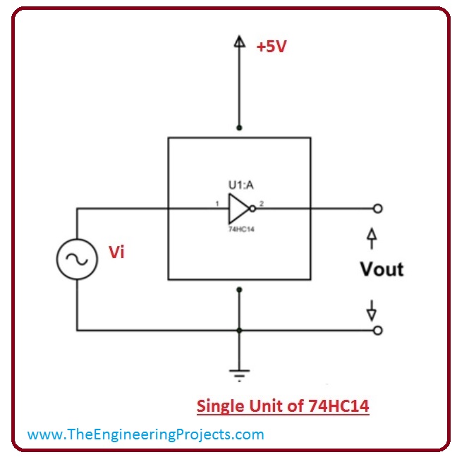
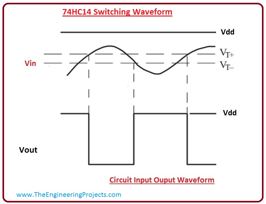
- We can see in the given diagram, the sinusoidal signal is given at the input and we receiving (Vout) as an output. The input, output graph is shown in the above diagram.
- The working principle of Schmitt trigger is very simple, the inverting Schmitt trigger's output is low only when input voltage values cross the threshold voltage (+Vt).
- We can see in the given diagram that the value of input voltage (Vin) is below the threshold voltage (Vt+), an output voltage is high. The value of the input voltage closer the value of the threshold voltage, the value of the output voltage shows low-value state.
- The value of output voltage remains low until the input voltage value is low to the threshold voltage. After this cycle continues.
- We can observe form diagram that the sinusoidal signal is our input and square wave is output. We can use every gate to get the output according to our requirements.
Switching Time of 74HC14
- Now, discuss switching time of 74HC14, in which we see how much time it take for switching.
- Every gate in 74HC14 takes some time to show output according to applied input. This delay of time is called switching time. For better understanding lets see switching diagram of 74HC14.
- There are two types of delays which occurs during switching. Which are Rise time (tPHL) and Fall time (tPLH).
- In a given diagram we can see that VoH becomes low when input reaches a threshold voltage and VoH becomes higher when the input voltage lower than the threshold voltage.
- We can observe from a graph that there is a delay between input as it is going high and Voh going low. This time delay is called Rise time (tPHL ). The value of rising time (tPHL ) is 95ns.
- We can also see from a picture that there is a time delay between logic input as it is going low and VoH is going high at the output. This time delay is called Fall time (tPLH ).
- All these delays occur at higher frequencies, if frequencies are below given frequencies, then there will be some major errors.

Applications of 74HC14
- These are some applications of 74HC14.
- It is the general purpose logic.
- It is used in PCs and notebooks.
- It is used in TV, DVD, Set Top Box.
- It is used for Networking.
- It is also used in Digital systems.
