

Hello, Students here I am present to cover an article on a series of Electronic devices and circuit theory. The foremost article of this series is Ideal diode vs practical diode. I try to elaborate on basic to modern theory related to the diode. This component act as fundamental to many important circuit devices such as rectifiers, transformers, etc. The question which we cover in this article are;
- What is a diode?
- How a diode is formed? Which methodology manufacturer utilized while the formation of the diode?
- What is the concept of doping and PN junction in diode theory?
- How does a Diode work?
- What type of biasing allows a diode to conduct? Under which situation of biasing diode offers a restriction while conducting?
- Upon which characteristics do we categorize the diode as an ideal diode and practical diode?
- Which factor makes a diode ideal? And how practical diode is different from an ideal diode?
Along with these questions, numerous questions may arise in your mind related to diode because it is a very vast concept in circuit theory. If you want to know the answer to these questions, keep sticking with our article. The best step taken by our platform for the easiness of our readers is to provide two things in a single platform. A short video of this article is also tried to cover on our YouTube channel. You may visit. The link is given at end of the article.
What is a diode?
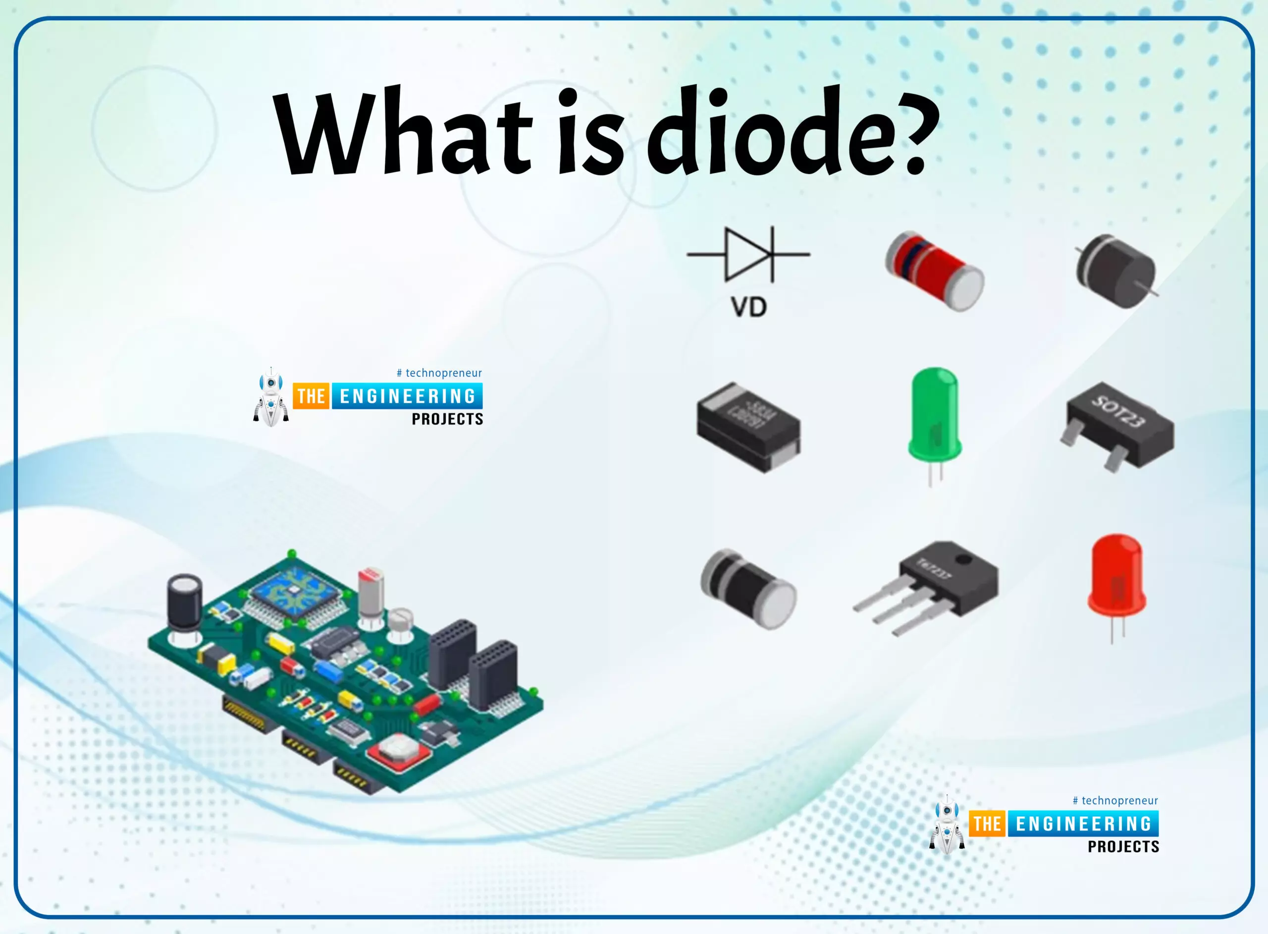
A diode is a two-terminal device that worked as a one-way conductor. A diode may assume as a simple solid-state component. This solid-state component is formed when the intrinsic semiconductor such as germanium or silicon Crystal is grown in such a way that one end is doped with pentavalent and the other end is doped with a trivalent impurity. It is also referred to as PN-junction Diode. Here word doped comes from techniques of doping which is used during the manufacturing of diode.
Doping
The process of adding an impurity to an intrinsic semiconductor I.e germanium and silicon. Semiconductors are those materials whose conductivity lies between a conductor ( good to conduct electricity) and an insulator ( bad to conduct electricity). To enhance the conducting capacity of semiconductors they are doped with different Impurities. Here the word impurity is used for those elements which are doped to pure semiconductor, after they are doped the germanium or silicon Crystal no longer remains pure.
Which element is used for doping?
Basically, elements from a fifth and third group of the periodic tables are commonly used in this process. Which refer to as pentavalent impurity (5the group) and trivalent impurity. Byword pentavalent means there are five electrons present in the outermost shell they lose one electron to complete their Octate and to become stable. That’s why these impurities are also named Donor impurity examples of such impurity are phosphorus, bismuth, etc. When we add such impurity to a semiconductor then N-type material is formed. Trivalent are those which have 3 electrons in the outermost shell and they need 1 electron to become stable due to this reason they are also named acceptor impurities. Examples of such impurities are Aluminum, Boron, etc. When they are doped with pure semiconductors then P-type material is formed.
How a diode is formed?
When intrinsic semiconductors is doped with two different Impurities then a junction is formed which I explain you in video of our Engineering prove t channel and I try to explain this also in my article;
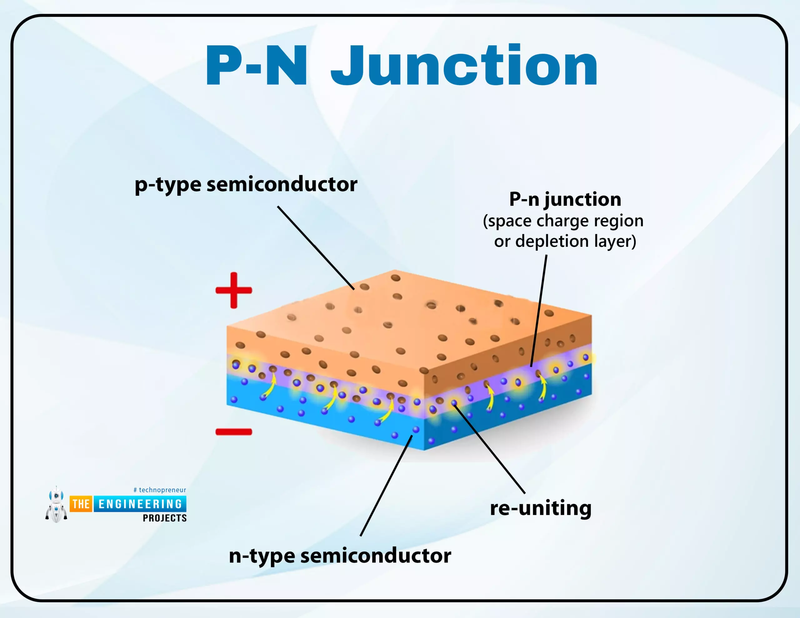
When an N-type material is combined with P-type material then a PN junction is formed. In N-type material, there is the availability of a large number of free electrons which act as a majority charge carrier and holes act as minority charge Carriers. While in P-Type materials the doped material belongs to a trivalent group, they need 1 more electron to complete their covalent bond tendency. To complete one hole an electron jump from one shell to another. This creates another hole in the second shell which results in more than holes these holes act as majority charge carrier and electrons act as a minority charge carriers in P-Types material. As soon as these material are combine electrons from the N-side start to attract toward holes in P-side where they both diffuse and as soon as electron diffuse in the P-side this leave behind a positive ion and holes from the P-side move toward N-side and leave behind a negative ion result information depletion layer where there is lack of Carrier but still, there is the availability of negative and positive ions. This creates a natural potential difference between the two sides, thus forming a junction which refer to as PN-junction. Given below energy diagram and other pictorial representation helps to understand my concept.
Symbolic representation of a PN junction diode.
Symbolically a diode is represented as follows:
How diode works
Under which biasing diode conduct and which biasing make diode poor to Conduct?
Biasing;
Biasing is a process in which to obtain the desire mode of operation we apply potential to both sides of the diode. This potential also helped us to control the width of the depletion layer.
Forward Biasing;
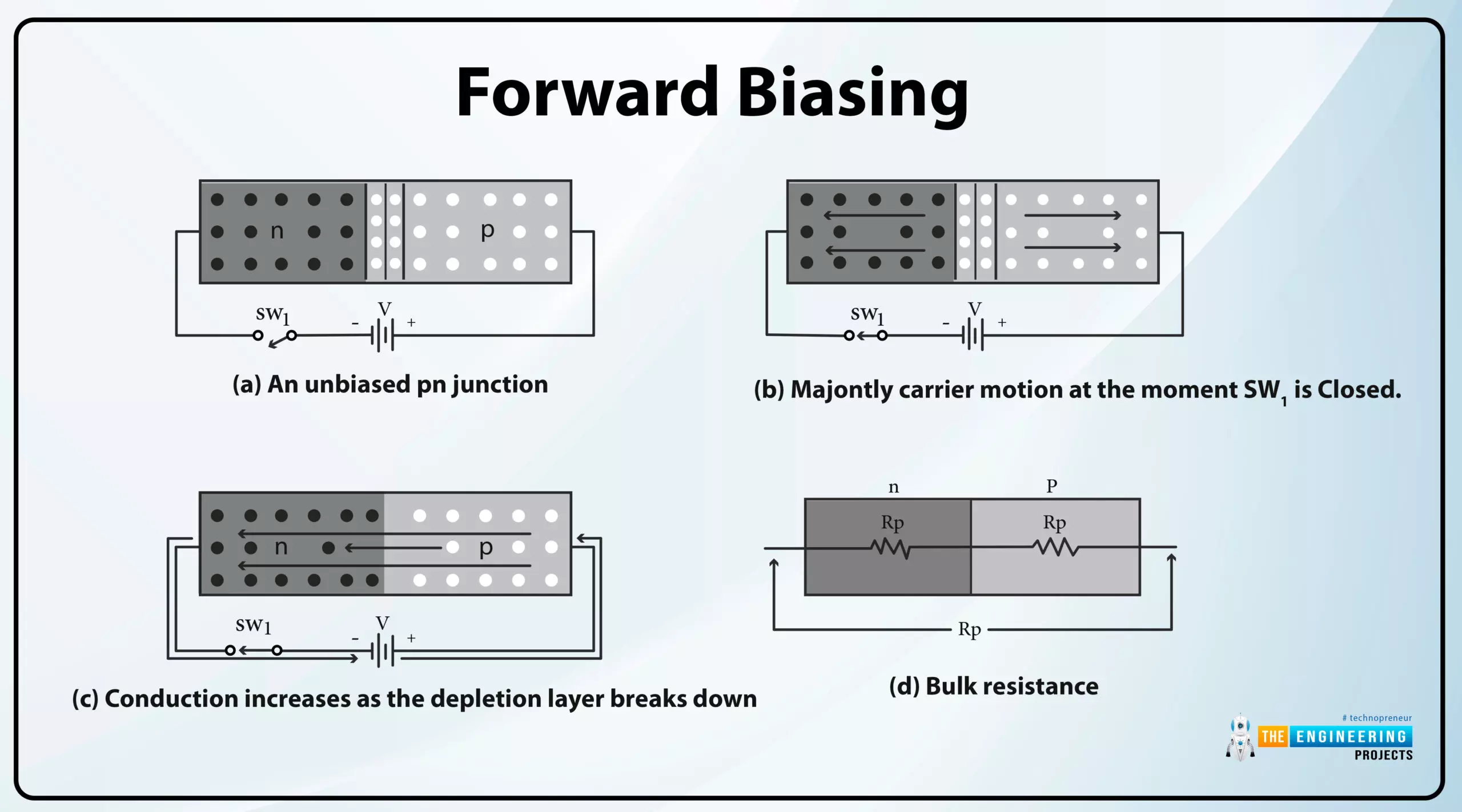
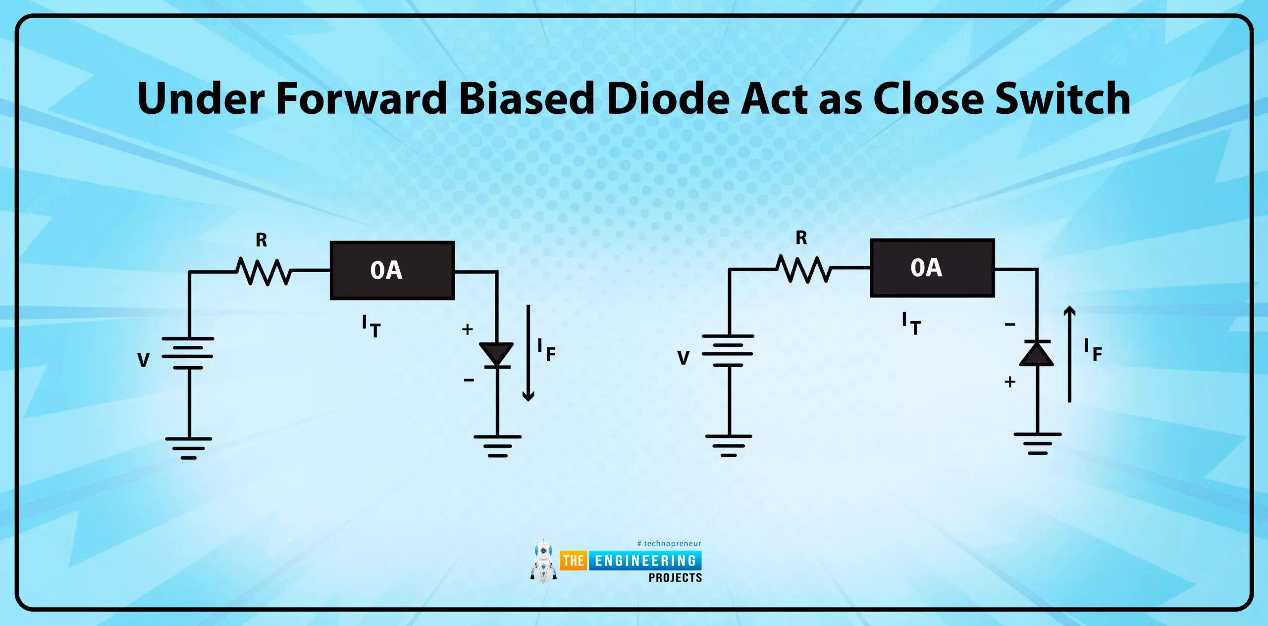
As shown in figure when biasing is applied in such a way that we provide the positive potential to cathode or P-Side of diode which makes it positive and negative potential of battery is connected with N-side of diode this makes the N-side more negative than P-side. This meets the necessary condition for a diode to conduct. This allows the flow of charges with little opposition almost negligible along with the depletion layer which reduces its width. Once a diode starts to conduct, there is slight opposition faced by carriers. This opposition is a referee to as bulk resistance. It combines the resistance of N-type and p-type. Its value is a most 5 ohm or less.
R(B)= R(N) + R(P)
As the value of R(B) is very low therefore there is little voltage drop across the resistance. Thus negligible in circuitry calculations. When the diode conduct fully the forward voltage becomes greater than the barrier potential. Typically the value of barrier potential or forward voltage for silicon and germanium are;
V(f) =0.7V for silicon
V(f)= 0.3V for germanium
Thus we can drive a diode to conduct by making the N-side more negative than the P-side of a diode.
Reverse Bias
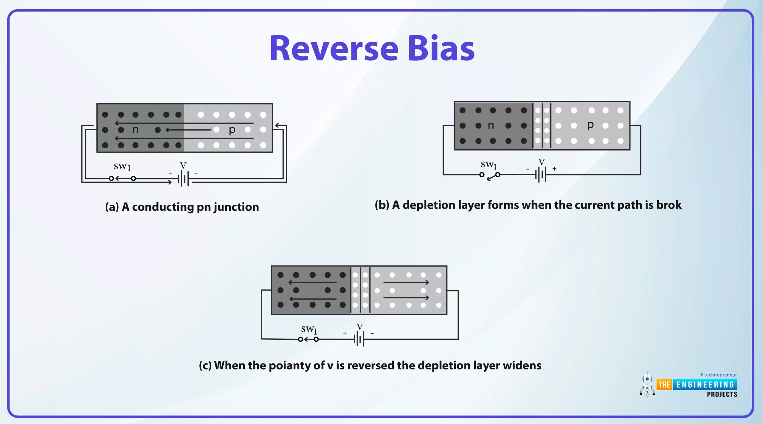
When the potential is applied in such a way that the N-side is connected to positive terminal and P-side of diode is connected to the negative terminal of the battery then no electron and hole move through the junction they attracted toward their own attached pole side of the battery thus enhancing the width of depletion layer, junction current becomes reduces to zero. This means that there is large opposition faced by carriers in reverse biasing. However, there is a small few Milliampere current drawn in reverse biased condition due to some thermal agitation process which causes electron and hole pair combination. We can set a reverse biased condition by applying a potential to the N-side such that it drives more positively than the P-side of diode.
The conclusion which we drawn from these two biasing methods is;
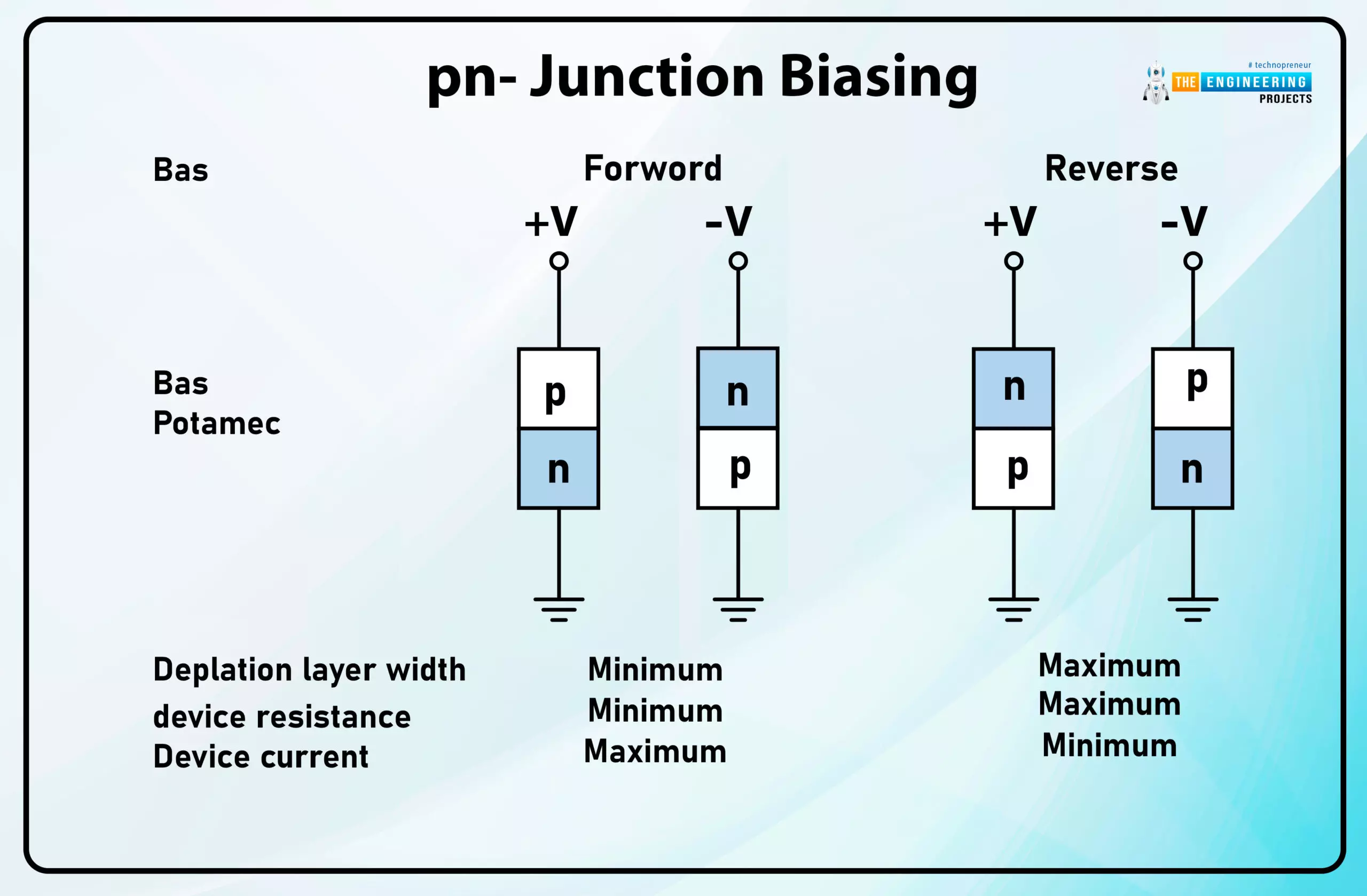
Under forward biased conditions n-type is more negative then p-type, depletion layer width, junction Resistance are at minimum value. And device current is at peak value. Under reverse bias every situation becomes reversed p-type is more negative than the n-side. The width of the depletion layer increase and junction resistance meet to peak value we can say it becomes infinite and the device current become negligibly zero.Want are the characteristics that make a diode ideal?
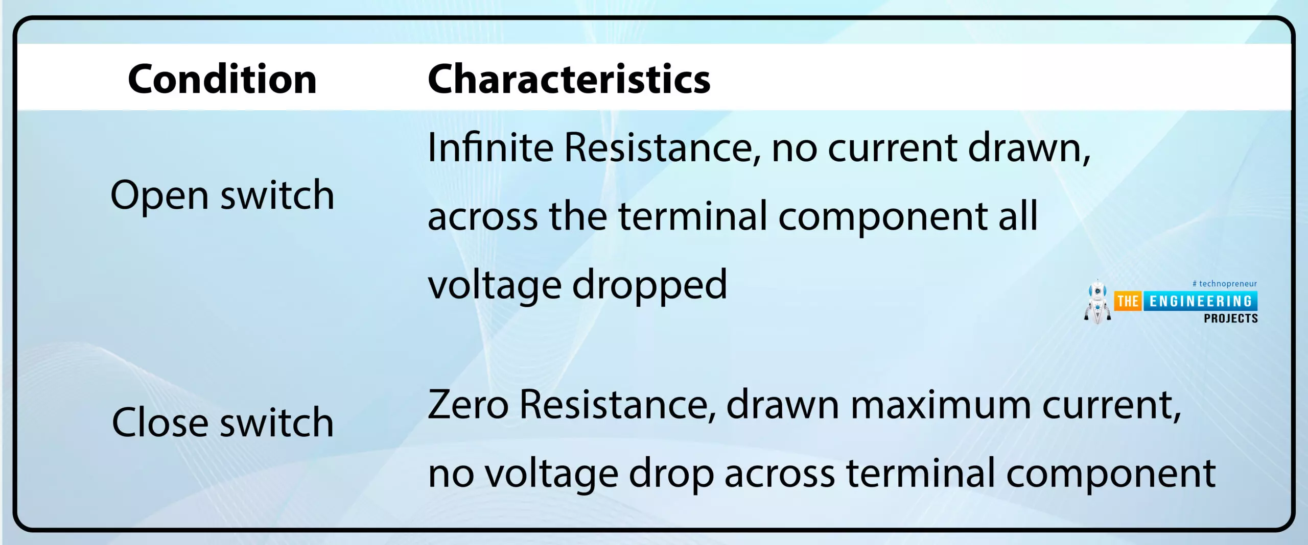
Ideal diode act as switch. There might be two possibilities which we attain while studying ideal diode. One is open switch and other is close switch. Let’s put a through back on some characteristics which a switch possess:
Ideal diode have following properties, which I also explain in my video whose link is given below of our article source.
Ideal diode can acts as a good conductor and good insulator under varying biasing schemes.
Under reverse biased condition it act as open switch;

- Infinite Resistance
- There is no flow of current across the junction. And diode acts as prefect insulator.
- All voltage dropped across terminal component.
Under forward biased diode act as close switch
which have following properties;
- Zero forward resistance
- Maximum current is dream from diode. AMD Diode acts as perfect conductor.
- No voltage drop across the components.
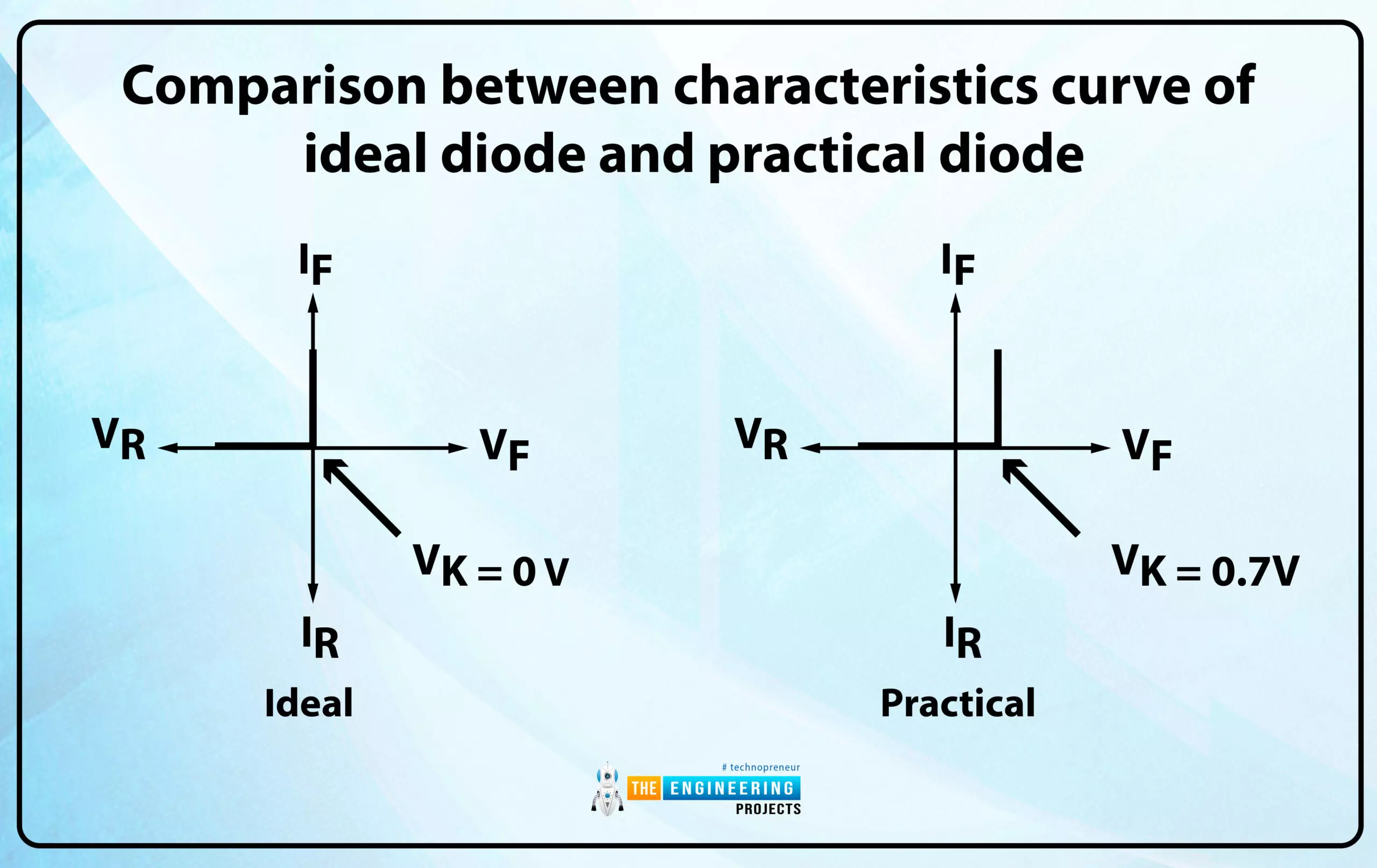
Characteristics curve of ideal diode
Now consider a characteristics algorithm for an ideal diode;
Characteristics curve of a circuit is the curve which is dream between the current and voltage to explain the manner in which device work under different situation.
Forward voltage is measured along positive x- axis and reverse voltage along negative x-axis. Similarly forward current and reverse current are measured along positive y-axis and negative y-axis respectively. 1st quadrant represent the forward bias region and 3rd quadrant represent reverse biased operating system. For vertical line in forward bias region the value of forward voltage increases with increase in forward voltage. For horizontal line in reverse bias mode we see that value of reverse current remains at zero level no matter what the value of reverse voltage. This implies diode act as perfect Insulator or open switch under reverse bias condition.

Now we discuss
how practical diode is different from ideal diode and what characteristics it posses?
(a) A practical diode can’t act as a perfect conductor and perfect insulator.
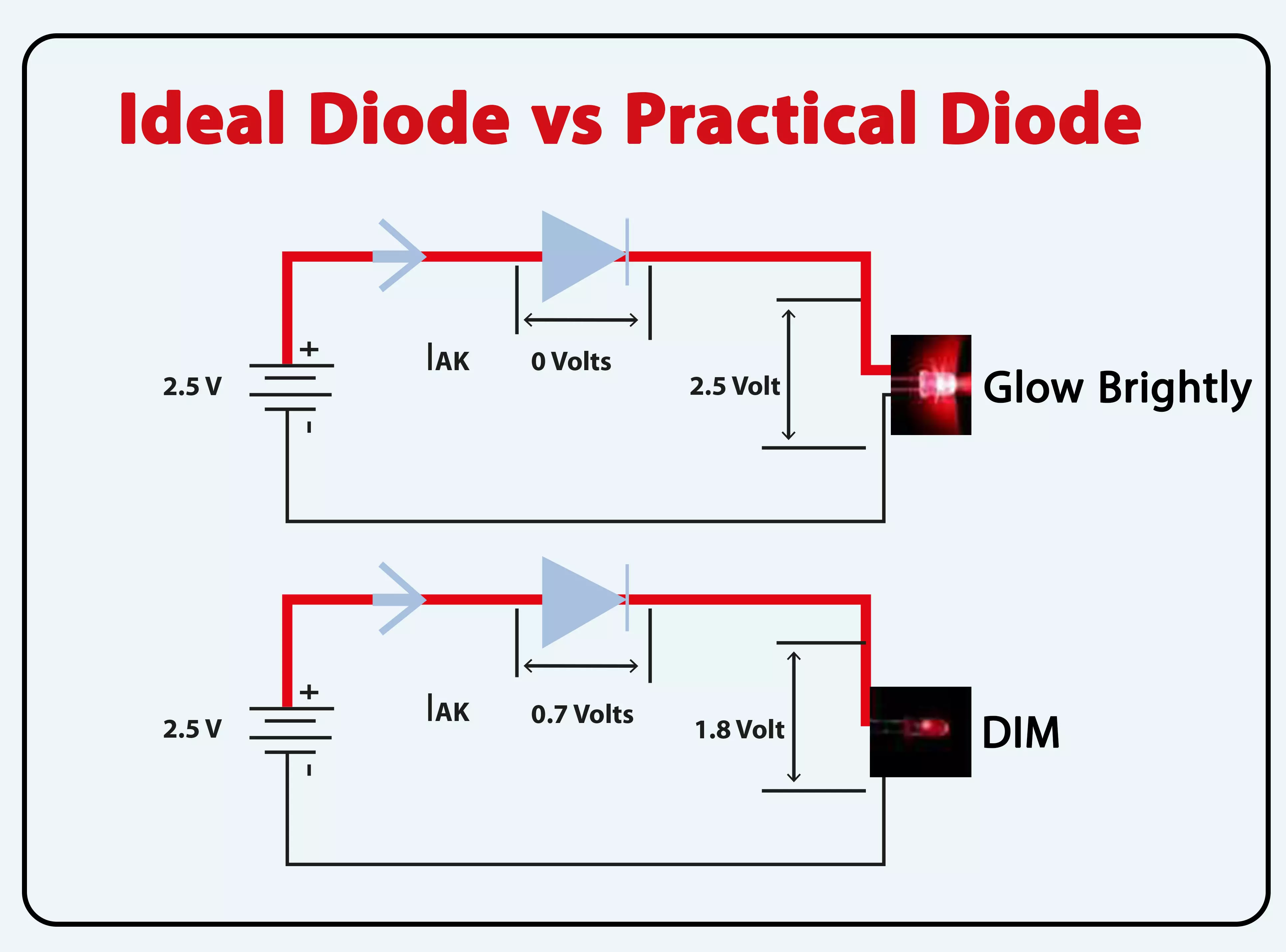
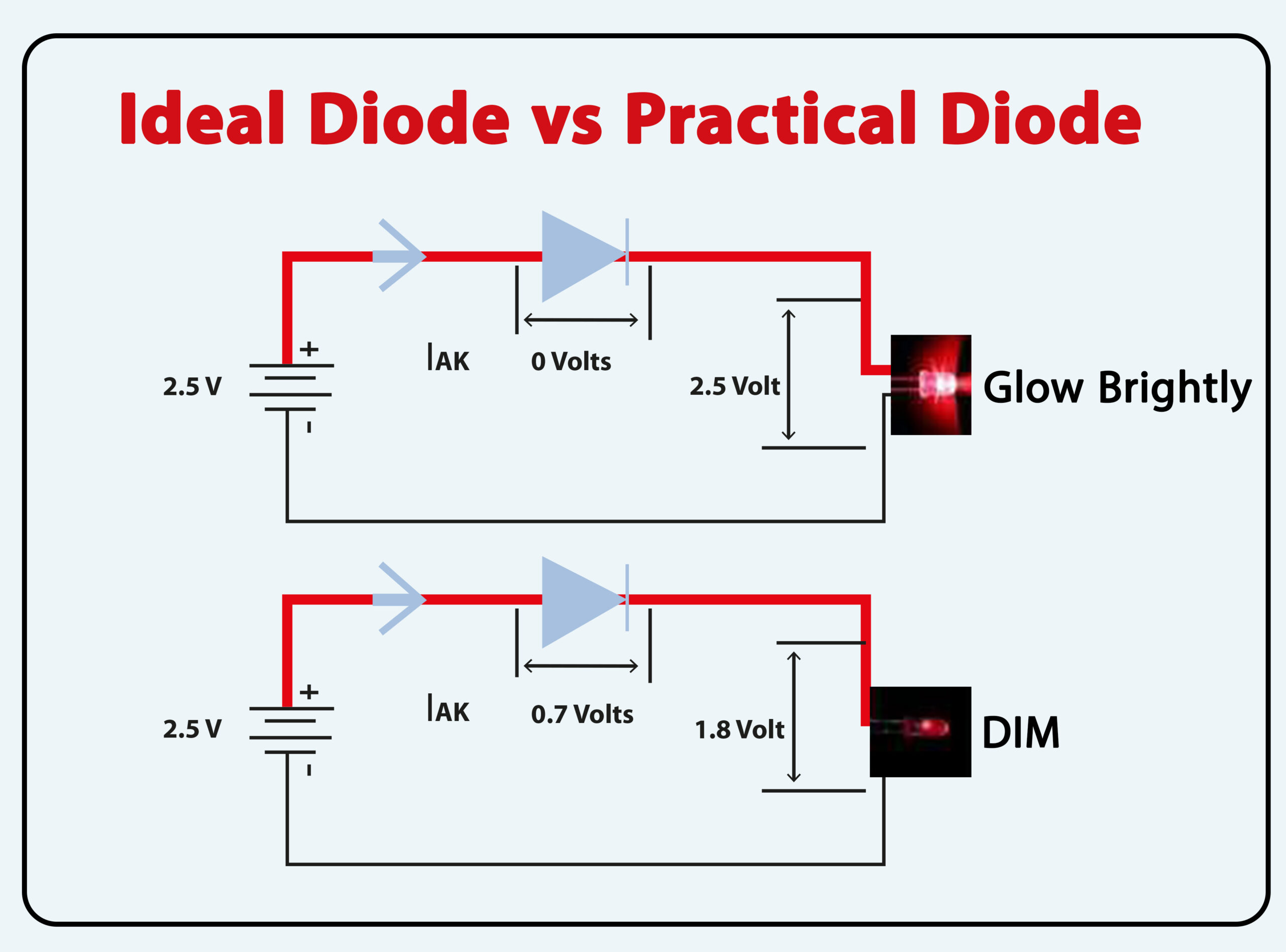
(b)Under reverse bias conditions there are a few milli-ampere current flows. Its value is very low. Now the question is why its Draws a small amount of current when reverse biased, it might be due to some thermal agitation process. Let’s try to explain this query. Consider the characteristics curve of the diode in both situations ideal and practical. in an ideal diode under reverse bias, the curve starts from the origin and there is no reverse current. And knee voltage is zero. Byword knee voltage we consider a point on the current-voltage curve at which there is a sudden increase or decrease of current. When a reverse voltage is increased beyond a limit then a breakdown occurs. Which break the electron-hole pair, and provides us a flow of free charge carrier due to this reason a small current is drawn even under reverse condition for practical diode due to electron-hole pair recombination. The value of knee voltage for silicon PN-junction is 0.7 V.
( c) In an ideal diode under forward biasing there is no voltage drop. While in practical diode there is a finite voltage drop across the terminal component whose value is different for silicon and germanium PN-junction.
(d) Piratical diode offers some finite Resistance under forward biasing which can’t be ignored and under reverse biased conditions there is no infinite Resistance.
The result we obtained about the Practical diode are:
(a) As Long as the knee voltage is not reached, the diode current is zero.
(b) When the knee voltage is achieved the diode begins to work and draws forward current.
Comparison between characteristics curve of ideal diode and practical diode
Lastly, there is an observable difference between the characteristics curve of both diodes.
In an ideal diode for forward biasing the forward current is maximum and the voltage drop is zero. And under reverse conditions no matter what’s the voltage, the reverse current is zero.
While in practical diode under forwarding biased, no current is drawn until the knee voltage that is 0.7 V is reached. Once this voltage is reached and the diode start to conduct the value of knee voltage is approximately equal to forward voltage I.e 0.7 regardless of the value of forwarding current.
The comparison between voltage and current values calculated in both diodes is summarized in below pictorial representation.
Some other considerations which we should make while dealing with practical diode are;
- Peak reverse voltage
- Average forward current
- Forward power dissipation
This is the article from the series of electronic devices and circuit theory. I hope this material might be helpful for you. If you have any queries you may mention your problem in the comment section. Thanks to All.
