Hi everyone! Thank you for viewing this article, I welcome you on board. In this post I’ll walk you through the detailed Introduction to BC546. BC546 is a low power NPN transistor mainly used for general purpose amplification and switching applications.
In this read you’ll study all nitty-gritty of BC546 transistor i.e. from pinout, pin configuration, and working principle to power ratings, key parameters, physical dimensions and applications. Keep reading.
Introduction to BC546
BC546 is a bipolar junction NPN transistor that finds applications in switching, amplification, impedance, H-bridge and current mirror circuits.
This transistor falls in silicon epitaxial planar transistor category which is generally divided into three groups A, B & C. This BC546 is available in group A & B.
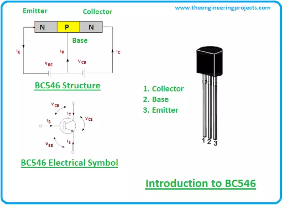
BC546 low power transistor mainly contains three terminals named emitter, base and collector. And all these terminals are different in terms of their doping concentration and are used for external connection with electronic circuits.
BC546 transistor contains three layers i.e. two N-doped layers and one P-doped layer. The P-doped layer resides between two N-doped layers. Plus, it carries two PN junctions where one is forward biased and other is reverse biased.
Unlike FET (Field-Effect Transistor) that is voltage controlled device, BC546 is a current controlled device where small current at the base terminal is primarily used for controlling the large current at both emitter and collector terminals.
1. BC546 Datasheet
Although, we are going to discuss everything related to BC546, in this tutorial but still its always wise to have a look at the datasheet.
You can download BC546 Datasheet by clicking the below button:
The collector voltage is much larger than the base voltage and emitter terminal is highly doped compared to base and collector terminals. When voltage is applied at the base terminals, it ignites the electron reaction between emitter and collector terminals.
3. BC546 Pin Configuration
Emitter current is a sum of both collector current & base current.
The small current at the base terminal is used to control large current at the emitter and collector terminals.
This transistor can be employed in three main configurations named:
Common base configuration.
Common emitter configuration.
Common collector configuration.
Common emitter configuration comes with exact voltage and current ratings required for amplification.
Forward current defines the nature of amplification. It is called amplification factor, or beta and denoted by ß. Which is a ratio between collector current and base current and it carries no unit. The amplification factor ranges from -110 to 800.
Similarly, current gain is a ratio between collector current and emitter current. It is known as alpha, denoted by a. The alpha value ranges from 0.95 to 0.99 but more often than not its value is taken as unity.
4. BC546 Working Principle
BC546 is a junction transistor where both electrons and holes are responsible for conductivity, electrons are majority charge carriers, however.
In NPN transistor base terminal is positive with respect to emitter and is usually used to control the number of electrons.
It gets biased and draws current when voltage is applied at the base terminal, thus controlling the large current at emitter and collector side.
Free movements of electrons plays a key role for conductivity and is mainly used to bridge the gap between emitter and collector where electrons are emitted by the emitter which are then collected by the collector.
In this NPN transistor current flows from collector to emitter unlike PNP transistor where current flows from emitter to collector.
5. BC546 Power Ratings
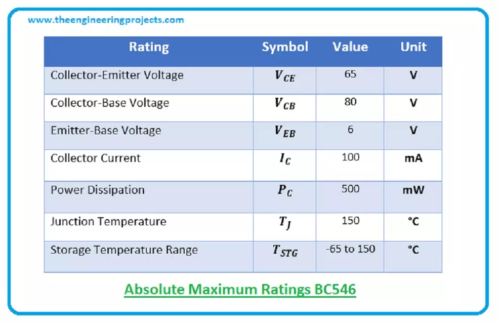
Absolute maximum power ratings of this NPN transistor are shown in the figure below:
Collector-Base voltage is 80V. And Emitter-Base voltage is 6V.
High Collector-Emitter voltage of 65V makes it the best pick for high voltage audio amplifier applications.
Collector current is 100mA with maximum power dissipation 500mW at temperature 25C.
These are stress ratings that, if increased from absolute maximum ratings, can severely affect the quality of the product, thus damaging the device.
Similarly, if these ratings are applied for the extended period of time, they can affect the device reliability.
The absolute maximum ratings are stress ratings with values measured at T = 25C
6. BC546 Modes & Key Parameters
The current directions and voltage polarities are opposite in both NPN and PNP transistors. If current flows in a clockwise direction in NPN transistor and carries positive polarity at the base terminal, it will flow in an anticlockwise direction in PNP transistor negative voltage polarity. Flow of electrons from collector to emitter in this NPN transistor depends on the biased voltage applied at the base terminal. Following are four modes of BC546 transistor:
Active mode.
Cut-off mode.
Saturation mode.
Reverse-active mode.
Base terminal is also called the active mode, and is mainly responsible for transistor action, where voltage is applied that draws small current which is then used to control large current at the emitter and collector terminals.
In cut-off mode transistor acts like an open switch and no current flows between the terminals.
Saturation mode acts like an ON switch where current flows from collector to emitter. In this condition the voltage difference between collector and emitter is zero.
In reverse active mode transistor acts like an active mode but here current direction is reversed, now it flows from emitter to collector.
7. BC546 Alternatives
BC546 contains following alternatives:
2SC4145
2SD1698
2SD1701
2SD1978
2SD1981
2SD2296A
2SD2213
HIT667
KTC1026
KTC3200
All transistors mentioned above are NPN transistors and are composed of silicon material. While its complementary types PNP transistors are BC556 & BC559.
8. BC546 Applications
BC546 is mainly used in the following applications:
It is used in linear amplifiers.
BC546 finds applications in H-Bridge circuits
Used for impedance circuits and current mirrors circuits
Also employed in oscillator circuits and Astable vibrators
Used in bistable multivibrators and comparator circuits
9. BC546 Physical dimensions
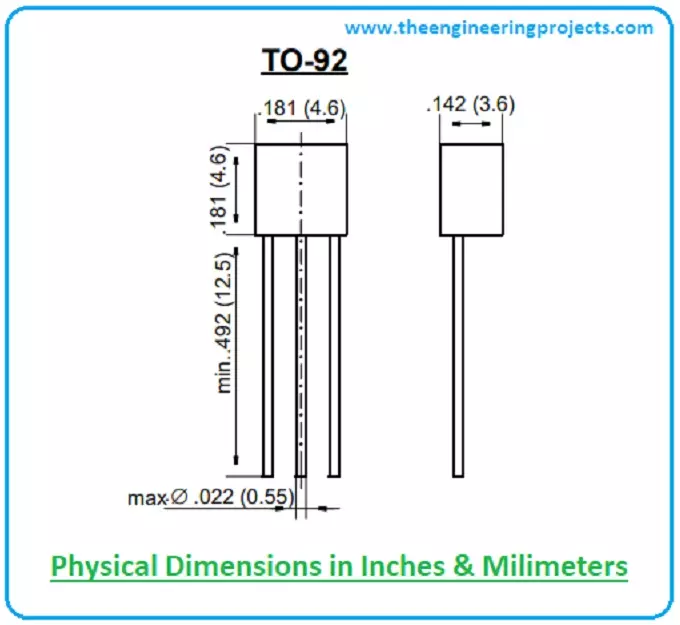
Following diagram shows the physical dimension of BC546:
All three terminals are 0.492in in length and 0.181in in width with distance between two terminals 0.142in. This transistor carries weight approx. 0.18g.
That's all for today. I hope you’ve got clear idea about BC546 transistor. If you are unsure or have any question, you can ask me in the section below, I'd love to help you the best way I can. You’re most welcome to keep us updated with your valuable feedback and suggestions. Thank you for your precious time.
syedzainnasir
I am Syed Zain Nasir, the founder of The Engineering Projects (TEP). I am a
programmer since 2009 before that I just search things, make small projects and now I am sharing my
knowledge through this platform. I also work as a freelancer and did many projects related to
programming and electrical circuitry. My Google Profile+Follow
Get Connected