74LS238 Datasheet, Pinout, Features, Working and Simulation

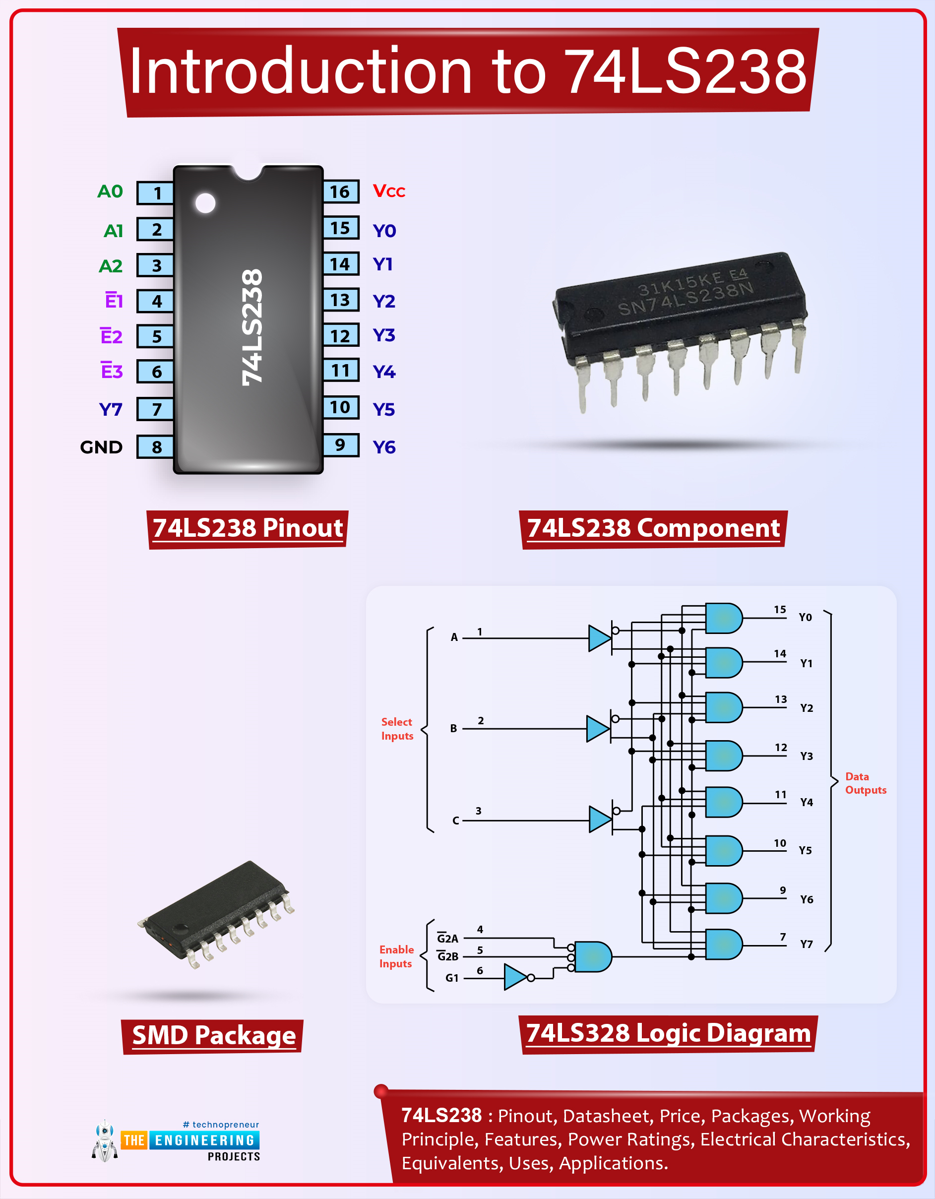
Hey readers! I hope you are doing great. Welcome to another article where we are discussing the integrated circuit device. Today, we’ll study the 74LS238 IC, which is a widely used component in different digital circuits as a multiplexer and demultiplexer. Multiple features of this IC, such as its low power performance and versatility, make it a good choice for electronic circuits. 

In this article, you will see the basic introduction of 74LS238, the datasheet of this IC, its working principle, the simulation in Proteus, and its applications in detail. There is a lot of information to understand about this 3 to 8 line decoder and we’ll shed light on all these topics from scratch so let’s start working on it.

Figure 1: Basic structure of 74LS238 IC

74LS238 Introduction

  • The 74LS238 is an integrated circuit that belongs to the transistor-transistor logic (TTL) family and is part of the Shcottkey series.
  • It is a 16-pin DIP IC and the LS in the name of this decoder indicates low-power performance.

  • It is a 3 to 8 line decoder and demultiplexer and generally, the following points are covered in its working:
    • It is designed to take three inputs in binary format only

    • The internal structure of this IC performs complex calculations of demultiplexing or decoding according to the circuit

    • On the output side, the inputs are converted into eight mutually exclusive outputs and the high value is only at one output

  • This IC is widely used in different digital circuits because of its versatility. 

  • It has a reliable, simple, and straightforward working nature. Moreover, it is also preferred to convert complex circuits into simple ones because of their fine structure and the ability to fit in multiple types of circuits. 

  • It has the feature of minimizing the effect of system decoding.  

74LS238 Datasheet

The details of the structure and functionalities of the 74LS238 IC can be understood from the details of its datasheet. Here are different points about this IC:

74LS238 Pinout Configuration

This IC has 16 pins that are packed in the dual inline package (DIP). Here is the diagram that describes its structure:

Figure 2: Pinout configuration of 74LS238

All the pin numbers have a specific name in alphanumeric format. The details of each pin and its description are given here:


Symbol

Pin Number

Description

Active State

A0

1

Address input

-

A1

2

Address input

-

A2

3

Address input

-

E1

4

Enable input

LOW

E2

5

Enable input

LOW

E3

6

Enable input

HIGH

Y0

7

Output

HIGH

Y1

9

Output

HIGH

Y2

10

Output

HIGH

Y3

11

Output

HIGH

Y4

12

Output

HIGH

Y5

13

Output

HIGH

Y6

14

Output

HIGH

Y7

15

Output

HIGH

GND

8

Ground (0 V)

-

VCC

16

Supply voltage

-


Table 1: Pinout configuration of 74LS238

74LS238 Function Table

The 74LS238 is used as the 3 to 8 line decoder. The binary combination of three inputs results in different outputs. Here is the detail in the form of the function table:

Enable Inputs

Select Input

Outputs

G1 

G2A

G2B

C

B

A

Y0

Y1

Y2

Y3

Y4

Y5

Y6

Y7

X

H

X

X

X

X

L

L

L

L

L

L

L

L

X

X

H

X

X

X

L

L

L

L

L

L

L

L

L

X

X

X

X

X

L

L

L

L

L

L

L

L

H

L

L

L

L

L

H

L

L

L

L

L

L

L

H

L

L

L

L

H

L

H

L

L

L

L

L

L

H

L

L

L

H

L

L

L

H

L

L

L

L

L

H

L

L

L

H

H

L

L

L

H

L

L

L

L

H

L

L

H

L

L

L

L

L

L

H

L

L

L

H

L

L

H

L

H

L

L

L

L

L

H

L

L

H

L

L

H

H

L

L

L

L

L

L

L

H

L

H

L

L

H

H

H

L

L

L

L

L

L

L

H

Table 2: Function table of 74LS238

74LS238 Alternatives

The following are some other devices that have similar features and can be used in place of 74LS238:

  • 74HC238 

  • SN74HCT238

  • LS238C

  • TS74HC238P

74LS328 Logic Diagram

We know that ICs are made of a combination of logic circuits. The internal structure of these ICs makes the concept of working of the IC clear. If you want to have the details of its structure, you can have a look at the logic diagram of 74LS238 in a positive state:

Figure 3: Logic diagram of 74LS238

If you want to learn this datasheet in detail, you can have a look at the linked article give here:

74LS328 Working Principle

The basics of the working of this IC in detail are shared with you so that you may know the expected outcomes when using the 74LS238:

74LS238 Input Combination

This IC consists of three inputs that take only binary information. It means the inputs are only in the form of 0 and 1. The combination of these numbers decodes the output line, where the signals will be high. 

74LS238 Decoding Logic

The decoding logic of the 74LS238 depends on the internal structure that varies from manufacturer to manufacturer. The logic diagram is shared with you in this tutorial. Different combinations of these logic gates are used to get the required output. 

This IC usually consists of AND and NOT gates that process the inputs together and provide the expected output at the output.

74LS238 Output Selection

The internal structure is responsible for setting one of the eight bits high. This is the basic expectation of this integrated circuit. After processing the input bits, only one output bit is selected where the HIGH signals are sent. All other bits remain low.

74LS238 Enable Control

There are three enable pins (E1, E2, and E3) that work as the master switch of the decoder. The functionality of each of these is given next:

  • The E1 and E2 pins work closely with each other and if any one of these is HIGH, the output is always HIGH, no matter what the inputs are. 

  • The pin E3 provides additional control over the output of the decoder. It is an important pin because it acts as the AND gate with three inputs and the overall output is HIGH only when the result of this AND gate combination is set to LOW. 

74LS238 Simulation in Proteus

If you want to check the working of this IC then a good option is the proteus simulation. Here, I have created a simple circuit of this IC that will help you understand how the output is generated with 74LS238:

Material Required


74LS238 Features and Specifications

Till now, I hope you have an idea of the working of this IC but I have created a table that clearly describes its features and specifications of 74LS238 at a glance:


Category

Feature

Description

General Information

Function

3-to-8 line decoder with active LOW outputs

Family

TTL (Transistor-Transistor Logic)

Logic Level

Low-power Schottky (LS)


Package Type

DIP (Dual In-Line Package) with 16 pins

Inputs

A0, A1, A2

Binary address inputs (3 lines)

E1, E2, E3

Enable inputs (3 lines, all must be LOW to enable outputs)

Outputs

Y0 to Y7

Active LOW decoded outputs (8 lines)

Key Specifications

Propagation Delay

15 ns typical

Power Dissipation

19 mW typical

Supply Voltage

4.75 V to 5.25 V

Operating Temperature

0°C to 70°C

74LS238 Physical Dimensions

Before designing the circuit with the 74LS328, it is crucial to know the dimensions of this IC. Here is the table that describes its exact size in metric and imperial units:


Dimension

Value (mm)

Value (inches)

Width

6.10

0.240

Length

9.91

0.390

Height

3.81

0.150

Lead Spacing

2.54

0.100

74LS238 Applications

The 3 to 8 line decoders have applications in multiple fields where the digital circuits are the basic devices. The main application of 74LS238 is in the form of a 3 to 8 line decoder and here are some examples of its applications:

74LS238 for Memory Address Decoding

In circuits like memory banks, an important process is to calculate the higher address bit. Here, the 74LS238 is widely used and its basic duty is to activate the most appropriate memory chip. In some cases, it also activates the specific memory location within that chip. 

74LS238 in Microprocessors

Some microcontrollers have limited input-output ports, therefore, ICs like 74LS238 are used to expand the availability of the pins by providing the decoding process. Through decoding, the microprocessor can successfully select the required device at a time.

74LS238 in the Display Control

In display devices where the output is created by stimulating the specific arrangement of the LEDs, the 74LS238 plays a crucial role. For instance, in the 7-segment display, 74LS238 can illuminate the particular segments. As a result, the output shows the particular digit. 

74LS238 in the Simplification of Circuits

The logic circuits consist of multiple logic gates and other related components. Logic gates are simple circuits and provide basic functionality but if the user wants to have a higher level of performance, there is a need for complex circuitry that is difficult to understand. The 74LS238 has built-in decoding functionalities therefore, using this IC in the logic circuit is a good idea to reduce the complexities of the circuit.

In this way, we have understood the basic information of the 74LS238 in detail. In this article, we have started from the scratch and learned about the introduction of the 74LS238 in detail. We saw the datasheet of this IC and understood the basic features in detail. We also created the simulation of 74LS238 in Porteus and in the end, we saw the physical dimensions and applications of this decoder. I hope this was a useful study for you and if you want to add more authentic information to it, you can contact us.

74LS164 Datasheet, Pinout, Features, Working and Simulation

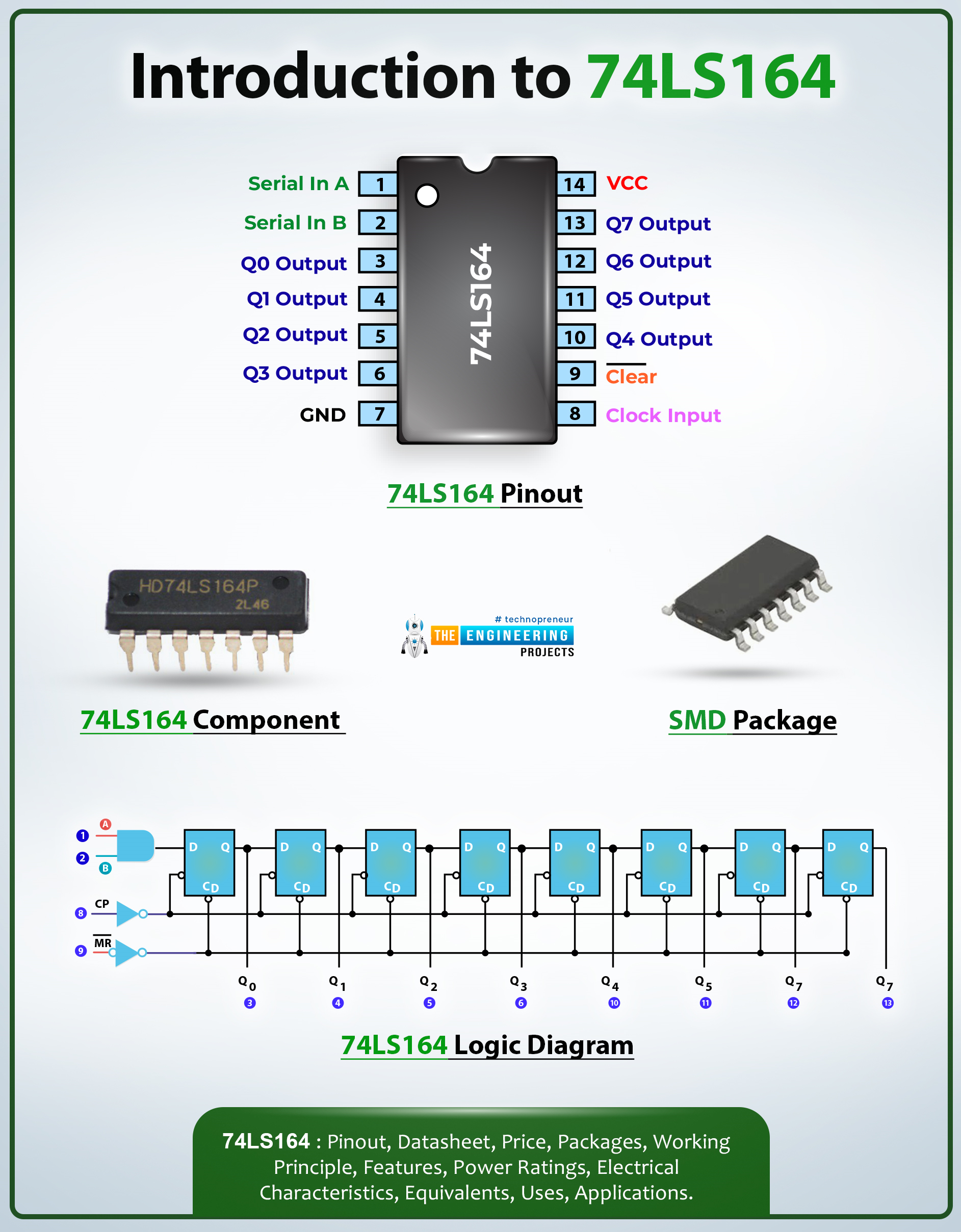
Hi pupils! Welcome to another article on integrated circuits. We have been studying different ICs in detail and today the topic is 74LS164. It is another important family member of the 74xx series of ICs and is widely used in different types of digital devices because it is a serial-in parallel-out shift register.

In this article, we’ll discuss the 74LS154 in detail. We’ll start with the introduction and after that, I’ll share a detailed datasheet with you that will help you understand the workings and basic structure of this app. After that, I’ll discuss the working principle and share a simple project of this IC in proteus. Moreover, I'll share the measurement of the dimensions of this IC and in the end, there will be the details of applications for 74LS164. This article has all the basic information about this IC and let’s start our discussion with its introduction

74LS164 Introduction

  • It is a synchronous reset register that takes the serial input but can process and represent the data in the parallel output. 

  • It belongs to the 74LS family; therefore, it is a low-power Schottky TTL logic circuit. 

  • It has an asynchronous clear.

  • It is a 14-pin dual inline package (DIP) and sometimes the package is a small outline integrated circuit (SOIC).

  • It acts differently in the situation. At the low logic level, it follows the logic given next:

    • It may inhibit the entry of new data 

    • At the next clock pulse, it resets the flip-flops to the low level

As a result, it has complete control over the incoming data. 

  • At the high logic level, any input enables other inputs and this determines the start of the first flip-flop.

  • This is one of the most simple and versatile registers; therefore, it has multiple applications in different fields where digital circuits are used.  

74LS164 Datasheet

The information about the datasheet of this IC will help you understand the basic information in detail. 

74LS164 Connection Diagram

The 14-pin package has a specific pin configuration. Each PIN has a specific name according to its function. This can be understood with the following connection diagram

  • It has the outputs on both sides of the IC.

  • A cut on the ground pin side indicates the right direction of the pin combination. 

  • It has two serial inputs. 

74LS164 Pinout Configuration

The details of the above diagram will be clear with the help of the following table:

Pin No

Pin Name

Description

1

A

Data Input 

2

B

Data Input 

3

Q0

Output pin

4

Q1

Output pin 

5

Q2

Output pin 

6

Q3

Output pin

7

GND

Ground Pin

8

CP

Clock Pulse Input

9

MR’

Active Low Master   Reset

10

Q4

Output pin 

11

Q5

Output pin 

12

Q6

Output pin 

13

Q7

Output pin 

14

Vcc

Chip Supply Voltage

Table 1: 74LS164 pinout configuration

74LS164 Sequential Logic Circuit Operations

The combination of the inputs in this IC results in different conditions. Here is the detailed table for this:

CP

DSM

MR

Operation

Description

Additional Notes

X

X

Clear (Asynchronous Master Reset)

It immediately clears all flip-flops to 0, regardless of clock or other inputs.

Overrides all other operations.

X

H

Hold (No Change)

Maintains the current state of the register.

It is useful for pausing data transfer or holding a specific value.

L

X

Load Parallel Data

Loads the parallel data inputs (A-H) into the register.

It occurs on the next rising clock edge.

H

H

Shift Right (Serial Input)

Shifts data one position to the right, with new data entering at the serial input (SER).

Occurs on each rising clock edge.

Table 2: 74LS164 Sequential Logic Circuit Combination

This can be understood with the following information:

  • CP (Clock Pulse) = It controls the timing of data transfer and operations.

  • DSM (Data Strobe Master) =  It enables parallel data loading when low.

  • MR (Master Reset)= It asynchronously clears the register when low.

  • X = It is the "don't care" condition, which means the input can be either high or low without affecting the operation.

  • ↑ = It represents a rising clock edge.

  • ↓= It represents a falling clock edge.

74LS164 Logic Diagram

The internal structure of any IC is much more complex than the connection diagram because ICs consist of a combination of different logic gates. Here is the logic diagram that displays the internal structure of the 74LS164:

Figure 3: 74LS164 Logic Diagram

Here, you can see how the basic logic gates combine to form the 74LS164.

74LS164 Timing Diagram

The operations and the clock shifting of the 74LS164 are understood with the following diagram.

Figure 4: 75LS164 Timing Diagram

This is a general representation of the timing diagram that can be understood with the help of the following points:

  • The rising edge clock pulse signal (CP) results in the shifting operation of the pulse. 

  • When the parallel load phase is applied to the parallel inputs, it affects the content of the shift register. 

  • The master reset signal clears the active low transition and clears the shift register asynchronously. 

If you want to know more details about the datasheet for 74LS164, then you can visit this:

74LS164 Circuit Diagram

The general representation of the circuit diagram is important to understand when you are using it in practical work. Here is the diagram that clearly specifies the working and pin connections of this IC.

Figure 5: Circuit diagram of 74LS164

74LS164 Working Principle

  • The 74LS164 has a pin named MR, which is a low active input master reset pin. The output of this pin remains in a low state until the state of the circuit is low. In such conditions, the values on the input do not affect its state. 

  • The MR pin is also referred to as the reset or clear mode pin. 

  • The procedure of the circuit’s working is completed only when the output of the MR pin is set high. 

  •  This IC has two serial input pins for all the functions. These pins are responsible for the versatility of this IC. 

  • In order to ignore any unintentional input signal, any unused input is set to high. 

  • In the event that the clock transition is set from low to high, the data in the IC is moved to one place on the right. The AND operation of the input pins A and B determines the new value of the right-most bit, Q0.

74LS164 Simulation in Proteus

Before ordering or testing this IC, a good practice is to learn how it works in the simulator. I am presenting a simple circuit of the 74LS164 IC in Porteus ISIS. The following are its details:

Component Required

  • 74LS164 IC

  • LEDs 

  • SW-SPDR (switch)

  • Power terminal

  • Ground terminal

  • Clock pulse

74LS164 Testing Project Steps

  • Open the Proteus software. 

  • Go to the pick library “P” option and choose the first three components one by one by typing their names and double-clicking on them.

  • Arrange these components on the screen.

  • Connect the components using the wire connections. 

  • Go to terminal mode from the left side of the screen and attach ground, power, and clock terminals on the required sites. 

  • The circuit should look like the following image:

Figure 6: Proteus Simulation of 74LA123

  • The connections must be created cleanly and clearly to ensure the right output. 

  • Click on the play button presented on the left side of the screen to start the simulation.

74LS164 Working of Project

Once the project is complete, you will see the following points:

  • The circuit does not show any output on the LEDs when the circuit is played. At this point, the LM317 does not get any input.

  • Once the negative input is provided to the switch, the LEDs start showing the output one after the other. This shows the logic HIGH on the bits after the regular interval. 

Figure 7: output of 64LS164 circuit with a switch on the negative side

  • Now, use the switch to provide the positive bit to the circuit, and the output on the LEDs will be shifted to the right. 

Figure 8: 74LS164 output when the plus side of the switch is on

  • As a result, the LEDs will show the LOW output one after the other and in the end, it will show the LOW output at every LED. 

If you want to test the circuit by yourself, download the simulation from the link given here:

74LS164 working Porteus Simulation

74LS164 Features and Specifications

The basic features and specifications of the 74LS164 are given next:

Characteristic

Value

Description

Operating Voltage

3V - 18V

Range of input voltage for proper operation

Maximum Supply Voltage

5.25 V

The absolute maximum voltage that can be applied to the device

Propagation Delay Time

25 ns

Time for a signal to travel through the device's internal circuitry

Maximum Clock Frequency

36 MHz

The highest clock rate at which the device can reliably function

Operating Temperature Range

0°C to +70°C

Environmental temperature range for reliable operation

Clock Buffering

Fully Buffered

Internal clock buffering for improved signal integrity and noise immunity

Available Packages

16-pin PDIP, GDIP, and PDSO

Different physical package options for PCB mounting

Logic Family

74LS (Low-power Schottky)

A specific logic family with tradeoffs in speed and power consumption

Power Consumption

(Typical) 75 mW

Average power is drawn during operation

Output Current

15 mA

The maximum current that can be sourced or sunk by the outputs

Fan-out

10 LS-TTL Loads

The number of logic gates that can be driven by a single output

Input Threshold Voltage

1.3 V

Minimum input voltage level to reliably recognize a logic high

Table 3: Features and Specifications of 74LS164

74LS164 Physical Dimensions

Just like other integrated circuits, the physical dimensions of the 74LS164 are also described in two units:
The metric dimensions are those in which the units used are the following:

  •  Millimetres (mm)

  • Centimeters (cm)

  • Meters

  • Kilograms

  • Seconds 

On the other hand, imperial units are those where the used units are the following:

  • Inches

  • Feet

  • Pounds

The dimensions of 74LS164 are given in the table:


Dimension

Metric (mm)

Imperial (inches)

Length

19.30 ± 0.30

0.760 ± 0.012

Width

6.35 ± 0.25

0.250 ± 0.010

Height

3.94 ± 0.25

0.155 ± 0.010

Pin spacing

2.54 ± 0.10

0.100 ± 0.004

Table 4: Physical dimensions of the 74LS164

74LS164 Application

As mentioned before, the 74LS164 is a versatile register IC. It has multiple applications mentioned here:

74LS164 in Arithmetic Logic Register

The feature of the 74LS164 to store memory temporarily is useful in applications like the arithmetic logic register. Moreover, on the same device, it also shifts the data within the arithmetic logic register. Here, the main purpose of using 74LS164 is to use serial or parallel data handling. 

74LS164 in Sequence Generator

The sequence generator requires the shifting and storing of the bit values. This can easily be done with the 74LS164 IC.

74LS164 in Digital Up and Down Counter

74LS164 is part of a large digital circuit. In digital up and down counters, this IC has applications because it has a sequential counting feature and when clock pulses are applied, it can decrement the values accordingly. 

74LS164 in Converter 

The basic feature of this IC is the serial to parallel output conversion. This feature makes it ideal for the circuit such as parallel to the serial output and vice versa.

So, in this article, we study the 74LS164 register IC in detail. We started with the basic introduction and then saw the details of the datasheet. There, we saw circuit diagrams, truth tables, logical circuits, and other related features to understand the basics of this IC. After that, we learned the working principle so that we could use it in the proteus simulation. Once we saw the results of the simulation, we studied the features and specifications of this IC, and in the end, we saw the applications of 74LS164. I hope we covered all the points but if something is missing, you can suggest it in the comment section.

74LS160 Datasheet, Pinout, Features, Working and Simulation

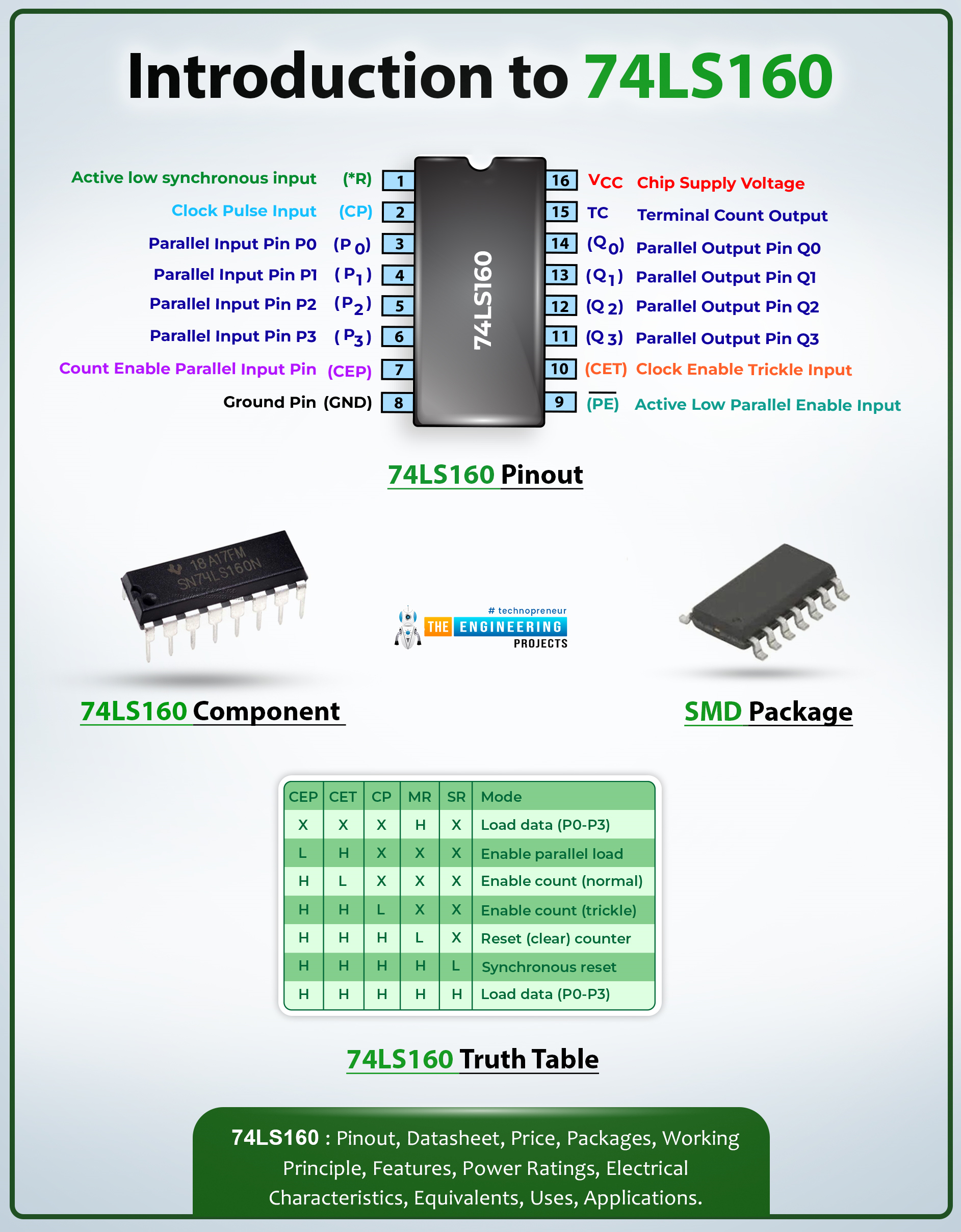
Hello students! Welcome to another tutorial on the integrated circuit in Proteus. Different integrated circuits are revolutionizing the electronic world and today we are discussing one of them. The core topic of this tutorial is the 74LS160 IC in the proteus but before that, we’ll understand the basics of this IC.

In this article, we’ll start learning the 74LS160 from scratch. We’ll see its introduction and datasheet in detail. You will see the truth table, logic diagram, and pinouts of this IC in detail, and then we’ll move on to the basic features of this IC. You will see the simulation of 74LS160 in Proteus and in the end, we’ll go through some important applications of this IC. Let’s move towards the introduction first.

Figure 1: Top view of 74LS160 IC

74LS160 Introduction

  • 74LS160 is an integrated circuit (IC) that is used as a counter in digital electronics.

  • It is a 4-bit binary synchronous counting device.

  • It belongs to the family of the 74xx series of ICs and the letters LS indicate that these belong to the low-power Schottky series. 

  • This IC is made with the transistor transistor logic (TTL) technology. 

  • It is an edge-triggered and cascadable MSI building block for multiple purposes, such as counting, memory addressing, frequency division, etc.

  • Moreover, it is widely used in digital circuits because it is presettable; that is, it can be used as the initial counter.

  • A feature of this series is that it has an asynchronous Master Reset (Clear) input that acts as an independent input, and the cock or other inputs do not control it.

74LS160 Datasheet

Before using any digital IC, it is important to understand its structure and datasheet. The details given below will help you understand the workings of this IC:

74LS160 Pinout Configuration

The 74LS160 is 16 in IC and here is its connection diagram, DIP:

Figure 2: Pinout configuration of 74LS160

You can see that each pin has a name and number associated with it. The details of each pin can be seen in the table given next:

Symbol

Name

Description

PE

Parallel Enable (Active LOW) Input

Enables parallel loading of data into the counter

P0–P3

Parallel Inputs

Four parallel data inputs for loading the counter

CEP

Count Enable Parallel Input

Enables counting when asserted (Active LOW)

CET

Count Enable Trickle Input

Enables counting when asserted (Active LOW)

CP

Clock (Active HIGH Going Edge) Input

Clock input for synchronous counting (Active on rising edge)

MR

Master Reset (Active LOW) Input

Resets the counter to 0 when asserted (Active LOW)

SR

Synchronous Reset (Active LOW) Input

Resets the counter synchronously (Active LOW)

Q0–Q3

Parallel Outputs (Note b)

Four parallel binary outputs represent the count

TC

Terminal Count Output (Note b)

Indicates when the counter reaches its maximum count

Table 1: Pinout configuration of 74LS160

74LS160 Logic Symbol

In different cases, when the 74LS160 is shown with the logic symbol given here:

Figure 3: Logic Symbol of 74LS160

Here, pin 16 is used for the power input and pin 8 is used as the ground. The names and numbers of the pins are the same as given before in the form of the table. 

74LS160 Truth Table

The truth table of this IC will help you understand the output of 74LS160 when the specific combination of inputs is fed into it. But before this, it is important to understand the following denotations in the table:

  • X = Don't-care condition

  • L = Logic low or ground

  • H = Logic high or positive voltage

  • CEP = Count Enable Parallel Input

  • CET = Count Enable Trickle Input

  • CP = Clock (Active HIGH Going Edge) Input

  • MR = Master Reset (Active LOW) Input

  • SR = Synchronous Reset (Active LOW) Input


CEP

CET

CP

MR

SR

Mode

X

X

X

H

X

Load data (P0-P3)

L

H

X

X

X

Enable parallel load

H

L

X

X

X

Enable count (normal)

H

H

L

X

X

Enable count (trickle)

H

H

H

L

X

Reset (clear) counter

H

H

H

H

L

Synchronous reset

H

H

H

H

H

Load data (P0-P3)

Table 2: Truth table of 74LS160

74LS160 Working Principle

The working principle of 74LS160 can be understood with the help of some important points about its internal structure. The basis of its working principle is to understand that when the clock pulse is applied to the 74LS160, it responds to it and counts the binary values.  Here are the important points to understand this:

74LS160 Counter Bits

Since the beginning, we have been mentioning that it is a 4-bit counter. It means it can count from 0000 to 1111 in binary numbers.  

74LS160 Clock Input

As with other integrated circuits, the counter responds to the clock pulse applied to its clock input. The rise in the clock input stimulates the counter operations. 

74LS160 Parallel Load Inputs

The parallel load inputs are denoted by P0 to P3. The counter allows the parallel loading of the data when the appropriate pattern of signals is applied at the input pins.

74LS160 Cascading

Cascading is the process in which two or more integrated circuits are connected with each other in such a way that the output of one circuit becomes the input of the other. This is done to enhance the working ability of the system or is crucial when higher calculations are required using the counter.

The 74LS160 allows the cascading process. In this case, the ripple carry output (RCO) is connected with the clock input of the next counter.

74LS160 Simulation in Proteus

Now, it is better to understand how to create the circuit of this IC in the Porteus simulator before using it in the circuit. Here is the way to create the circuit:

Material Required

  • 74LS160 

  • Switch

  • LED

  • Clock

  • Ground

  • Power

Procedure

  • Fire up the proteus software. 

  • Choose the first three components from the list given above. 

  • Place them in the working area to create the circuit.

  • Now, go to terminal mode from the left side of the screen and choose ground terminal. Place it in the respected area. 

  • Repeat the above step for the power terminal. 

  • Now go to generation mode and choose the Dclock. 

  • Place the clock on pin 2 of IC. 

  • Connect the component through the connecting wires. 

  • The circuit must look like the image given here:

Figure 4: Proteus Circuit for 74LS160

  • The circuit is now ready to work. Click on the play button to start the working of the circuit. 

74LS160 Circuit Working

  • The switches are used to provide the input signal to the circuit. When the switch is on, the input signal to the respective pin is HIGH, otherwise low.

  • At the start, the LEDs are working in a particular manner that the output is on all the pins in a particular pattern. 

Figure 4: Changing the input of the 74LS160 circuit

  • Change the input through the switches and you will observe the change in the output.

  • You will observe a change in the values of output when the signal on the input signals is changed.

Figure 5: Getting the output of the 74LS160 Circuit simulation

  • The inputs and outputs are the same as given in the truth table.  

If you want to have the design of the Proteus project I am using, then you can download it through the link given next:

Proteus simulation for the basic working of 74LS160

74LS160 Features and Specifications

The 74LS160 has different modes and studying all of these will help you to understand the features and specifications. 

74LS160 Counting Mode

  • On reaching the clock edge, a pulse propagates that stimulates the counter to work. 

  • The master-slave FF is the pulse that triggers the master-slave flip-flop structure of this IC. The state of the internal logic circuit is changed according to the structure of the IC. The details of these inputs are given in the table given before. 

  • The logic gates of flip-flops determine the output of the IC. Usually, the output depends on the following factors:

    • The current state of the pins

    • Previous inputs of pins

    • Feedback connections.

  • In some versions, 75LS160 has the decade working, which means these can provide values between 0 and 9.

  • The state of the master flip flop is transferred to the corresponding slave flip flop after some time. This is done to provide a stable and more synchronized output. 

74LS160 Preset Mode

  • During the processing, the low signals on the load input activate the logic path of the IC. 

  • All the values in the data inputs are transferred directly to the respective flip-flops. 

  • The process of overriding the current counter bypasses the internal counter logic. It also sets the counter’s desired initial values and this is done by presetting the counter.  

74LS160 Reset Mode

  • The reset pin is the active low pin, which means the output is reset when this pin has a zero value.

  • The clearing of the flip flop is the situation when all the FFs are forced to reset their values, no matter what the values on their inputs or what the values of the clock are.

74LS160 Carry Out (CO)

  • The logic gates in the structure of the integrated circuit determine the internal structure of the flip flops. These are particularly useful for the transition from 1001 to 0000, which is 9 to 0 in the decimal numbers. 

  • When the transition of the carry-out goes high, it indicates that the count cycle is complete. 

  • The carryout pulse can be used in the cascading counter to enhance the working ability of the circuit using 74LS160.

74LS160 Physical Dimensions

If you want to use the 74LS160 in your circuits, you must know the physical dimensions of this IC. There are two basic units to measure the physical dimensions of devices like ICs:

Metric Package

In the metric package, only metric units are used to represent the calculations. The following are some of the basic units in this system:

  • Millimetres (mm)

  • Centimeters (cm)

  • Meters

  • Kilograms

  • Seconds 

Usually, in the representation of the physical dimensions of the ICs, like 74LS160, millimeters are used for metric packages. 

Imperial Package

The imperial units are also known as the British imperial units. The popular units in the imperial packages are:

  • Inches

  • Feet

  • Pounds

The physical dimensions of the ICs in the imperial package are mostly inches. Here is the table that clearly shows the physical calculations of the 74LS160 IC:

Dimension

Metric (mm)

Imperial (inches)

Length

19.30 ± 0.30

0.760 ± 0.012

Width

6.35 ± 0.25

0.250 ± 0.010

Height

3.94 ± 0.25

0.155 ± 0.010

Pin spacing

2.54 ± 0.10

0.100 ± 0.004

Table 3: Physical dimensions of 74LS160

74LS160 Applications

The following are some prime applications where the 74LS160 is extensively used:

74LS160 as Digital Counter

The most common example of the application of this IC is to use it as a digital counter. When the clock pulse is applied to this IC, it represents the binary counting values. This is not only used as it is but usually other logic gates are combined with it to get the complex calculator to work. 

74LS160 Frequency Divider  

The frequency divider is the circuit that is designed to determine the value of frequency after dividing it by the power of 2. This circuit is incomplete without the 74LS160 IC. 

74LS160 Timer Circuits

This IC is incorporated into the time circuits, where its main job is to generate a time delay. Moreover, it also triggers specific events based on certain conditions. These conditions are set during the design process of the circuit. 

74LS160 in Sequential Logics

In the sequential logic, the 74LS160 is used as the counter. The output of this IC is used as the input of some other devices and this creates the basis of the sequential logic circuits.

74LS160 in Signal Processing Circuits

Signal processing is an important field where complex circuits are used. This IC is used in devices for signal processing where counting and timing functions are required.

Hence, today, we have seen the details of the 74LS160 Integrated Circuit. We started with the basic introduction of this IC and understood the structure and output of every pin through its datasheet. Through the logic diagram, logic circuit, truth table, and the pinouts of this IC we understood the details of its functionalities. Moreover, we saw its basic features and mode of operation. The physical dimensions of this IC made clear the domains of its usage in different circuits. We saw the simulation of the 74LS160 in the proteus and in the end, we shed light on different applications where the 74LS160 plays a vital role. I hope you have understood all the information but if you feel something missing or have any questions, you can ask us.

74LS138 - 3 to 8 Line Decoder IC | Datasheet, Working and Simulation

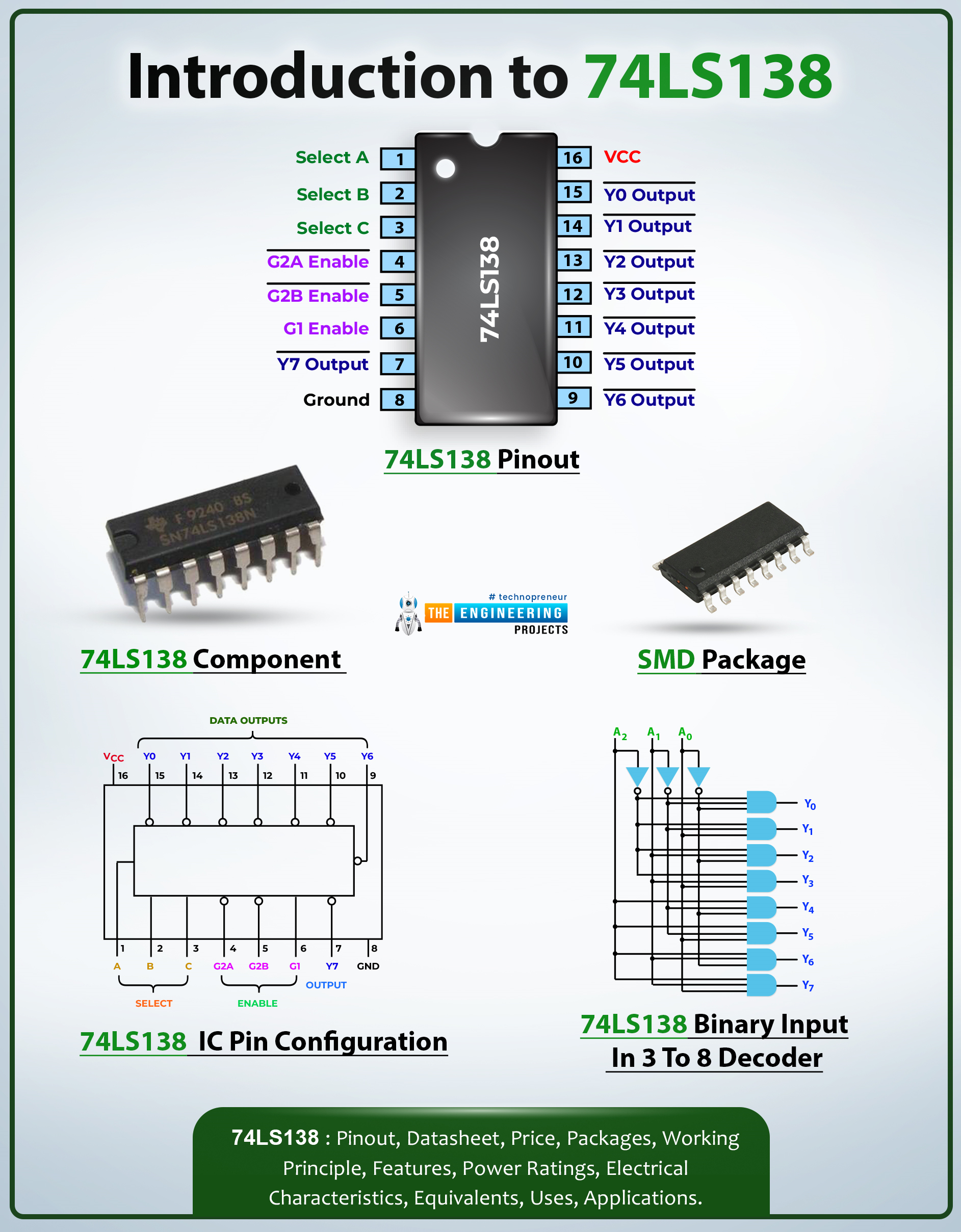
Hello students! I hope you are doing great. Today, we are talking about the decoders in the proteus. We know that decoders are the building blocks of any digital electronic device. These electronic circuits are used for different purposes, such as memory addressing, signal demultiplexing, and control signal generation. These decoders have different types and we are discussing the 3 to 8 line decoders.

In this tutorial, we will start learning the basic concept of decoders. We’ll also understand what the 3-to-8line decoders are and how we connect this concept with the 74LS138 IC in proteus. We’ll discuss this IC in detail and use it in the project to present the detailed work. 

Where To Buy?
No.ComponentsDistributorLink To Buy
174LS138AmazonBuy Now

What is a 3 to 8 Line Decoder?

A three to eight line decoder is an electronic device that takes three inputs and based on their combination, provides one of its eight outputs. In simple words, the 3 to 8 line decoder gets three inputs and reads the binary combination of its input. As a result, the single output is obtained at the output of the decoder. Here are the basic concepts to understand its working:

Binary Input in 3 to 8 Decoder

A 3 to 8 line decoder has three input pins which are usually denoted as A, B and C. These correspond to the three bits of the binary code.  The term binary means these can only be 0 or 1 and no other digits are allowed. This can be the raw bits from the user or can be the output signal from the circuits’ device that becomes the input of the decoder.

Outputs of 3 to 8 Decoder

The 3 to 8 decoder has eight possible output pins. These are usually denoted as Y0, Y1, Y2,..., Y7  and the output is obtained only at one of these pins. The output depends on the binary combination of the input provided to it. In large circuits, its output is fed into any other component and the circuit works. 

Functionality of 3 to 8 Decoder

As mentioned before, the combination of the binary input decides the output. Only one of the eight output pins of the decoder gets high which means, only one output has the value of one and all others are zero. The high pin is considered active and all other pins are said to be inactive. 

Truth Table of 3 to 8 Decoder

The truth talbe of all the inputs and possible output of 3 to 8 decoders are given here:

Input MSB (A)

Input B

Input LSB (C)

Active Output

Y0

Y1

Y2

Y3

Y4

Y5

Y6

Y7

0

0

0

Y0

1

0

0

0

0

0

0

0

0

0

1

Y1

0

1

0

0

0

0

0

0

0

1

0

Y2

0

0

1

0

0

0

0

0

0

1

1

Y3

0

0

0

1

0

0

0

0

1

0

0

Y4

0

0

0

0

1

0

0

0

1

0

1

Y5

0

0

0

0

0

1

0

0

1

1

0

Y6

0

0

0

0

0

0

1

0

1

1

1

Y7

0

0

0

0

0

0

0

1

Here, 

MSB= Most significant bit

LSB= Least significant bit

I hope the above concepts are now clear with the help of this truth table. 

Introduction to 74LS138 Decoder 

The 74LS138 is a popular integrated circuit IC that is commonly used 3 to 8 line decoder. It is one of the members of 74LS therefore, it is named so. The 74LS is a group of transistor transistor logic (TTL) chips. The basic feature of this IC is to get three inputs and provide the signal on only one pin of the output automatically based on the binary inputs. In addition to the input, output, and functionality of the 74LS138, there are some additional features listed below:

Features of 74LS138

  • The 74LS138 has the cascading feature which means, two or more 74LS138 can be connected together to enhance the number of output lines. The circuit is arranged in such a way that the output of one 74LS138 IC becomes the input of the other and as a result, more than one ICs can work together. 

  • The structure of this IC is designed in such a way that it provides high-speed operation. It is done because the decoders are supposed to decode the input so quickly that its output may stimulate other functions of the circuits. 

  • The TTL compatibility of the 74LS138 makes it more accurate. The LS in its name indicate that these are part of low-power shotkey series therefore, these can be operated at the 5V power supply. This makes it ideal for multiple electronic circuits and these do not require any additional device to get accurate power. 

  • These ICs are versatile because they come in different packages and the users can have the right set of ICs depending on the circuit he is using. Two common packages of this IC are given next:

    • DIP (Dual Inline Package)

    • SOP (Small Outline Package)

  • It has multiple modes of operation therefore, it has versatile applications. 

74LS138 IC Pin Configuration

Before using any IC in the circuit, it is important to understand its pinouts. The 73LS138 has the 16 pins structure that which is shown here:

The detailed names and features of these pins can be matched with the table given below:

Pin Number

Pin Name

Pin Function

1

A

Address input pin

2

B

Address input pin

3

C

Address input pin

4

G2A

Active low enable pin

5

G2B

Active low enable pin

6

G1

Active high enable pin

7

Y7

Output pin

8

GND

Ground pin

9

Y6

Output pin 6

10

Y5

Output pin 5

11

Y4

Output pin 4

12

Y3

Output pin 3

13

Y2

Output pin 2

14

Y1

Output pin 1

15

Y0

Output pin 0

16

VCC

Power supply pin

74LS138 in Proteus

The structure and working of this IC can be understood by creating a project with it and for this, we have chosen the Porteus to show the detailed working. Here are the steps to create the project of a 3 to 8 line decoder in Proteus:

  • Open your Proteus software.

  • Create a new project. 

  • Go to the pick library by clicking the “P” button at the left side of the screen. It will show you a search box with details of the components. 

  • Here, type 74LS138 and you will see the following search:

  • Double click on the IC to collect it on your devices. 

  • Selecting this IC, click on the working sheet to place it there. 

You can see the pins and labels of this IC. 

Designing a 3 to 8 Line Decoder with 74LS138

The 74LS138 requires some additional components to be used as a decoder. Here is the project where we are using it as 3 to 8 line decoder:

Components Required

  • 74LS138 IC

  • 8 LEDs of different colors

  • Switch SPDT

  • Switch  SPST

  • Switch Mom

  • Switch (simple)

  • Connecting wires

Procedure

  • Go to the pick library and get all the components of the circuits one after the other. 

  • Set the 74LS138 IC in the working area.

  • On the left side of the IC, arrange the switches to be used as the input devices.

  • On the left side of the IC, arrange the LEDs that will indicate the output. 

  • Go toto the terminal mode from the left side of the screen and arrange the ground and power terminals with the required devices. 

  • The circuit at this point must look like the following image:

  • Connect all of these with the help of connecting wires. For convenience, I am using the labels to have better work:

  • Once you have connected all the components, the circuit is ready to use. In the left bottom corner, search for the play button and run the project. 

  • Change the input with the help of switches and check for the output LEDs. You will see the circuit works exactly according to the truth table. 

Working of 74LS138 IC in Proteus

  • The 74LS138 is designed to be used as a 3 to 8 line so there is no need to connect different ICs and components to design the working of this decoder.

  • The input and output pins are present with this IC therefore, the user simply connects the switches as an input device. A switch has only two possible states that are either on or off therefore, it is an ideal way to present the binary input. 

  • Usually, LEDs are used as the output devices so that when they get the signal, they are turned on and vice versa. 

  • The ground and power terminals are used to complete the circuit. 

  • Pins 4, 5, and 6 are called the enabled pins. These are labeled as E1, E2, and E3 pins. Out of these, E1 and E2 are considered as the active low pins which means, these are active only when they are pulled down. On the other hand, the E3 is considered an active high; hence it activates the output only when it is pulled high. 

  • Once the circuit is complete, the user can change the binary inputs through the switches and check for the output LEDs. 

  • The combination of inputs results in the required output hence the user can easily design the circuit without making any technical changes. 

Today, we have seen the details of 74LS138 decoder IC in Proteus. We started with the basic introduction of a decoder and saw what is the 3 to 8 line decoder isdecoder. After that, we saw the truth table and the features of a 3 to 8 line decoder. We saw how 74LS128 works and in the end, we designed the circuit of a 3 to 8 line decoder using 74LS138. The circuit was easy and we saw it working in detail. If you have any questions, you can ask in the comment section.

2SC2240 Datasheet, Pinout, Power Ratings, Equivalents & Applications

Hello Everyone! Happy to see you around. In this post today, we’ll cover the 2SC2240 NPN Transistor. We will have a look at the 2SC2240 Datasheet, Pinout, Power Ratings, Equivalents & Applications.

Electrons are the majority charge carriers in this NPN transistor, in contrast to PNP transistors, where holes are the majority carriers. The 2SC2240 comes with a power dissipation of 0.3W, the amount of energy this transistor dissipates while operating in the forward-biased state, while the collector current is 0.1A means it can support load up to 0.1A.

This NPN transistor contains 3 terminals, named:

  1. Emitter
  2. Collector
  3. Base

If the voltage at the base terminal is above 0.7V, the transistor will get forward-biased and the current will start flowing from Collector to Emitter terminal. If the base voltage is less than 0.7V, it will remain reverse-biased.

So, let's have a look at the 2SC2240 NPN Transistor in detail. Let’s get started:

2SC2240 NPN Transistor

  • The 2SC2240 is a bipolar junction transistor that belongs to the NPN transistor family.
  • This component is mainly used for switching and amplification purposes and comes in a TO-92 package.
  • 2SC2240 comes with three layers, with one p-doped layer between two n-doped layers.
  • The two n-doped layers represent the Collector and Emitter, while the p-doped layer represents the Base Terminal.

  • This device contains three terminals: the base, collector, and emitter. The collector terminal collects the electrons coming from the base side and the emitter terminal emits the electrons into the base terminal.
  • The NPN transistors contain two junctions known as collector-base junction and emitter-base junction.
  • The transistor is said to operate in a Forward-Biased state, when the collector-base junction is reverse-biased, while the emitter-base junction is forward-biased.
  • When a negative voltage is applied at the emitter side and a positive voltage is available at the base terminal then we can make the emitter-base junction forward biased.

NPN vs. PNP: A Quick Recall

  • Bipolar Junction Transistors(BJTs) are categorized into two types i.e. NPN transistors and PNP transistors. This is a bipolar transistor, which means both electrons and holes play a role in the conductivity process inside the transistor.
  • But electrons are the major carriers in NPN transistors while in the case of PNP transistors, holes are the major carriers.
  • NPN transistors are preferred over PNP transistors because the mobility of electrons is more efficient than the mobility of holes.
  • These bipolar devices are called current-controlled devices, in opposition to MOSFETs, which are called voltage-controlled devices and carry terminals like a drain, source, and gate.

2SC2240 Datasheet

It’s wise to go through the 2SC2240 datasheet before you apply this device to your electrical project.

2SC2240 Pinout

The following figure shows the 2SC2240 pinout.

This component contains three terminals named: 1: Emitter 2: Collector 3: Base

  • These terminals differ in terms of size and doping concentration and are used for external connection with the electronic circuit. The emitter side is highly doped and the base side is lightly doped and the collector terminal is moderately doped.
  • The collector terminal dissipates more energy compared to the other two terminals. It is bigger in size compared to base and emitter terminals. The large surface area of the collector side guarantees more heat dissipation.

2SC2240 Working Principle

The base is responsible for the transistor action. When voltage is applied at the base terminal, it will bias the device and as a result, the current will flow from collector to emitter terminal. As this is an NPN transistor so here current will flow from the collector to the emitter side and in the case of the PNP transistor current will flow from the emitter to the collector side. These bipolar devices are not symmetrical in nature. This projects if we exchange the emitter and collector pins then these terminals will start working in reverse active mode and will stop working in forward active mode. The different doping concentrations of these pins are the reason this device lack symmetry.

2SC2240 Power Ratings

The following table shows the 2SC2240 power ratings.
Absolute Maximum Ratings of 2SC2240
Pin No. Pin Description Pin Name
1 Collector-emitter voltage 120V
2 Collector-base voltage 120V
3 Base-emitter voltage 5V
4 Collector current 0.1A
5 Power dissipation 0.3W
6 Current gain 200 to 700
7 Operating and storage junction temperature range -55 to 125C
  • If these ratings are applied more than the required time, they can affect the device reliability.
  • The collector-current is 0.1A which defines the amount of load this component can support.
  • The power dissipation is 0.3W which represents the amount of energy released during the working of this component.
  • The current gain ranges from 200 to 700 which is the amount of current this device can amplify.
  • The operating and storage junction temperature ranges from -55 to 125C.
  • The emitter-base voltage is 5V represents the voltage required to bias this component. The collector-base voltage and collector-emitter voltage both are 120V.
  • When using this device, make sure these ratings don’t exceed the absolute maximum ratings else they can damage the device.

2SC2240 Equivalents

The following are the 2SC2240 equivalents.
  • 2SC3201
  • 2SC3245A
  • 2SC3200
  • 2SC3245
  • 2SC2459
  • KTC3200
Before applying alternatives into your projects, double-check the pinout of these equivalents as the pinout of 2SC2240 might differ from the pinout of the alternatives. The 2SA970 is a complementary PNP transistor to the 2SC2240.

2SC2240 Applications

The following are the 2SC2240 applications.
  • Incorporated in modern electronic circuits.
  • Used in Bistable and Astable multivibrators circuit.
  • Used in voltage regulator circuits.
  • Used in a common power amplifier.
  • Used in electronic Ballasts.
  • Used in energy-saving lights.
  • Employed to support loads under 0.1A.
  • Used in the high switching power supply.
  • Used in high-frequency power transform.

2SC2240 Physical Dimensions

The following diagram shows the 2SC2240 physical dimensions.

With physical dimensions, you can evaluate the space required for this device in the electrical project.

That’s all for today. Hope you find this article helpful. Feel free to share your valuable feedback and suggestions around the content we share. They help us produce quality content based on your needs and requirements. If you’re unsure or have any questions, you can approach men in the section below. I’m happy and ready to help you the best way I can. Thank you for reading this post.

KSC1845 Datasheet, Pinout, Power Ratings, Equivalents & Applications

Hi Guys! I welcome you on board. In this post today, we’ll discuss the KSC1845 NPN Transistor. We will have a look at the KSC1845 Datasheet, Pinout, Power Ratings, Equivalents & Applications in detail. As it's an NPN transistor, electrons are the majority charge carriers and thus play a major role in conductivity. KSC1845 is mainly used for fast-switching and amplification purposes.

NPN transistor carries 3 terminals, known as:

  • Emitter
  • Collector
  • Base

If the applied voltage at the base terminal exceeds 0.7V, it will forward bias this NPN transistor and the current will start to flow from Collector to Emitter. If the base voltage is less than 0.7V, KSC1845 will remain in the reverse-biased state.

I suggest you buckle up as I’ll discuss the KSC1845 NPN Transistor in detail. Let’s get started:

KSC1845 NPN Transistor

  • The KSC1845 is a bipolar junction transistor that falls under the NPN transistor family.
  • It is made of silicon semiconductor material and comes in a TO-92 package.
  • The NPN transistors carry two junctions known as emitter-base junction and collector-base junction.
  • When the emitter-base junction is forward-biased and the collector-base junction is reverse-biased, the transistor starts to conduct.
  • KSC1845 Pinout, Symbol and SMD Package are shown in the below figure:

  • We can make the emitter-base junction forward-biased, by applying a negative voltage at its Emitter and a positive voltage at its Base.
  • KSC1845 contains three layers where one p-doped layer sits between two n-doped layers. The p-doped layer represents the base terminal while the other two n-doped layers represent Collector and Emitter.
  • In a forward-biased state, the Emitter emits the electron into the Base while the Collector collects the electrons coming from the Base.

NPN vs PNP

KSC1845 is a Bipolar Junction Transistor, so let's quickly recall it:

  • The bipolar junction transistors come in two types i.e. NPN transistors and PNP transistors. Both holes and electrons play a role in carrying out the conductivity process inside the transistor.
  • In PNP transistors, holes are the majority charge carriers, while in NPN transistors, electrons are the majority charge carriers.
  • Know that the mobility of electrons is better than the mobility of holes, that's why NPN transistors are preferred over PNP transistors for a range of applications.
  • These bipolar(BJT) components are called current-controlled devices in opposition to MOSFETs, which are considered voltage-controlled devices and carry terminals like a drain, source, and gate.

KSC1845 Datasheet

Before you incorporate this device into your electrical project, it’s wise to go through the KSC1845 datasheet that details the main characteristics of the device. Click the link below to download the KSC1845 datasheet.

KSC1845 Pinout

The following figure shows the KSC1845 pinout.

This component contains three terminals named: 1: Emitter 2: Collector 3: Base All these terminals are used for the external connection with the electronic circuit. These terminals differ in terms of size and doping concentration. The base side is lightly doped and the emitter side is highly doped while the collector side is moderately doped. The collector side dissipates more energy because it is bigger in size compared to other terminals. The large surface area of the collector side ensures more heat dissipation.

KSC1845 Working Principle

The base side is the main region that initiates the transistor action. When voltage is applied at the base terminal, it will bias the device and as a result, current starts flowing from collector to emitter side. These bipolar devices are not symmetrical in nature. Which means if we exchange the emitter and collector sides then these terminals will stop working in forward active region and start working in reverse active mode. The different doping concentrations of these terminals ensure the lack of symmetry.

KSC1845 Power Ratings

The following table represents the KSC1845 power ratings.
Absolute Maximum Ratings of KSC1845
Pin No. Pin Description Pin Name
1 Collector-emitter voltage 120V
2 Collector-base voltage 120V
3 Base-emitter voltage 5V
4 Collector current 0.05A
5 Power dissipation 0.5W
6 Current gain 200
7 Operating and storage junction temperature range -55 to 150C
  • When using this device, make sure these ratings don’t exceed the absolute maximum ratings else they can damage the device.
  • Plus, if these ratings are applied more than the required time, they can affect the device reliability.
  • The collector-current is 0.05A which shows the amount of load this device can support.
  • The power dissipation is 0.5W which represents the amount of energy released during the working of this component.
  • The current gain is 200 which shows the amount of current this device can amplify.
  • The collector-base voltage is 120V and the collector-emitter voltage is 120V. The emitter-base voltage is 5V represents the voltage required to bias this component.

KSC1845 Equivalents

The following are the KSC1845 equivalents.
  • FJV1845

Before applying alternatives into your projects, double-check the pinout of these alternatives as the pinout of KSC1845 might differ from the pinout of the equivalents.

The KSA992 is a complementary PNP transistor to the KSC1845.

KSC1845 Applications

The following are the KSC1845 applications.
  • Incorporated in modern electronic circuits.
  • Used in high-frequency power transform.
  • Used in electronic Ballasts.
  • Used in voltage regulator circuits.
  • Used in a common power amplifier.
  • Used in Bistable and Astable multivibrators circuit.
  • Used in energy-saving lights.
  • Employed to support loads under 0.05A.
  • Used in the high switching power supply.

KSC1845 Physical Dimensions

The following diagram shows the KSC1845 physical dimensions.

The KSC1845 physical dimensions help you evaluate the space required for this component in the electrical project.

That’s all for today. Hope you find this article helpful. If you’re unsure or have any questions, you can pop your comment in the section below. I’m ready to help you the best way I can. Feel free to share your valuable feedback and suggestions around the content we share. They help us produce quality content based on your needs and requirements. Thank you for reading the article.

2SC1345 Datasheet, Pinout, Power Ratings, Equivalents & Applications

Hi Guys! Hope you’re well today. In today's tutorial, we will have a look at the 2SC1345 NPN Transistor. We will also discuss 2SC1345 Datasheet, Pinout, Power Ratings, Equivalents & Applications. As this is an NPN transistor, the conductivity is mainly carried out by electrons as the major charge carriers. 2SC1345 is mainly used for switching and amplification purposes.

Let's first recall NPN transistors: NPN transistor comes with 3 terminals, named:

  1. Emitter
  2. Collector
  3. Base

If the voltage at the base terminal is above 0.7V, the NPN transistor gets forward biased & starts conducting i.e. current will flow from the Collector to Emitter terminal. If the Base voltage is less than 0.7V, it remains reverse-biased.

So now let’s get started with the 2SC1345 NPN Transistor.

2SC1345 NPN Transistor

  • 2SC1345 is a bipolar junction transistor that belongs to the NPN transistor family.
  • It is composed of silicon semiconductor material and comes in a TO-92 package.
  • 2SC1345 contains three layers where one is a p-doped layer and the other two are n-doped layers. The p-doped layer stands between the two n-doped layers.

  • This device contains three terminals named: the base, collector, and emitter. The small current change at the base side is used to produce a large output current at the remaining terminals.
  • The bipolar junction transistors are available in two types i.e. NPN transistors and PNP transistors. Both holes and electrons play a role in the conductivity inside the transistors the reason they are called bipolar devices.
  • However, these devices differ in terms of major charge carriers. In the case of NPN transistors, electrons are the major charge carriers and in PNP transistors holes are the major charge carriers.
  • These bipolar devices are called current-controlled devices in opposed to MOSFETs that are termed voltage-controlled devices and contain terminals like a drain, source, and gate.
  • It is important to note that the mobility of holes is less efficient than the mobility of electrons the reason NPN transistors are preferred over PNP transistors for a range of applications.

2SC1345 Datasheet

Before you apply this component to your electrical project, it’s wise to scan through the 2SC1345 datasheet that features the main characteristics of the device. Click the link below to download the 2SC1345 datasheet.

2SC1345 Pinout

The following figure shows the 2SC1345 pinout.

This component contains three terminals named: 1: Emitter 2: Collector 3: Base These terminals carry different doping concentrations. The base side is 10-times more doped than the collector side. The emitter side is highly doped and the collector terminal is lightly doped.

2SC1345 Working Principle

When voltage is applied at the base terminal, it will bias the device and as a result, current starts flowing from collector to emitter terminal.
  • Know that, bipolar junction devices are not symmetrical in nature. This means if we exchange the emitter and collector terminals then these terminals will stop working in the forward active region and start working in reverse active mode.
  • The non-symmetry of these devices is due to the different doping concentrations of all three terminals.

2SC1345 Power Ratings

The following table represents the 2SC1345 power ratings.
Absolute Maximum Ratings of 2SC1345
Pin No. Pin Description Pin Name
1 Collector-emitter voltage 50V
2 Collector-base voltage 550V
3 Base-emitter voltage 5V
4 Collector current 0.1A
5 Power dissipation 0.2W
6 Base current 0.05A
7 Operating junction temperature range 150C
  • The collector-emitter voltage is 50V and the collector-base voltage is 550V. The emitter-base voltage is 5V which is the voltage required to bias the device.
  • The collector-current is 100mA which means it can support load under 100mA.
  • The power dissipation is 0.2W which is equal to the amount of energy released during the functioning of this component.
  • The current gain is 250 to 1200 which is the amount of current this device can amplify.
  • When working with this device, make sure these ratings don’t exceed the absolute maximum ratings else they can damage the device.
  • Moreover, if these ratings are applied more than the required time, they can affect the device's reliability.

2SC1345 Equivalents

The following are the 2SC1345 equivalents.
  • 2SC2240
  • KSC1845FTA (Fairchild)
Before incorporating these devices into your projects, double-check the pinout of these alternatives as the pinout of 2SC1345 might differ from the pinout of the equivalents.

2SC1345 Applications

The following are the 2SC1345 applications.
  • Used in electronic Ballasts.
  • Used in a common power amplifier.
  • Used in voltage regulator circuits.
  • Incorporated in modern electronic circuits.
  • Used in Bistable and Astable multivibrators circuit.
  • Used in energy-saving lights.
  • Used in high-frequency power transform.
  • Used in the high switching power supply.
  • Employed to support loads under 0.1A.

2SC1345 Physical Dimensions

The following diagram shows the 2SC1345 physical dimensions. The 2SC1345 physical dimensions give you the idea to evaluate the space needed for this device to incorporate in the electrical project. That’s all for today. Hope you find this article helpful. If you have any questions, you can approach me in the section below. I’m happy and willing to help you the best way I can. Feel free to share your valuable feedback and suggestions around the content we share so we keep producing quality content based on your needs and requirements. Thank you for reading the article.

D13005K Datasheet, Pinout, Power Ratings, Equivalents & Applications

Hello Everyone! Hope you’re well today. In today's tutorial, we will have a look at D13005K NPN Transistor. We will also study D13005K Datasheet, Pinout, Power Ratings, Equivalents & Applications. As its an NPN transistor, so major charge carriers are electrons. D13005K is mainly employed for switching and amplification purpose. Let's first recall NPN transistors: NPN transistor consists of 3 terminal, named as:

  • Emitter.
  • Collector.
  • Base.
If we provide voltage > 0.7V at base terminal, NPN transistor gets forward biased & starts conducting. If Base voltage < 0.7V, it remains reverse biased. So now let’s get started with D13005K NPN Transistor:

D13005K NPN Transistor

  • D13005K is a bipolar NPN transistor, mainly used for amplification and switching purposes.
  • It contains three layers where two n-doped layers surround one p-doped layer.
  • This device is made of silicon semiconductor material and comes in a TO-220 package.

  • D13005K contains three terminals named base, collector, and emitter. All these terminals are different in terms of doping concentrations.
  • The small current at the base side is used to control the large current at the emitter and collector terminals.
  • These transistors are called bipolar because both electrons and holes play role in the conductivity inside the transistor.
  • Bipolar junction transistors are divided into two main types i.e. NPN and PNP transistors.
  • In the case of NPN transistors, electrons are the major charge carriers while holes are major charge carriers in PNP transistors.
  • The bipolar junction transistors are the current-controlled devices in contrast to MOSFETs that are voltage-controlled devices that come with terminals named: drain, source, and gate.
  • The NPN transistors are preferred over PNP transistors because the mobility of electrons is better than the mobility of holes.
  • While in the case of NPN transistors the current flows from the collector to emitter terminals and it flows from emitter to collector terminal in the case of PNP transistors.

D13005K Datasheet

It is wise to go through the datasheet of the device before incorporating this component into your electrical project. The datasheet comes with the main characteristics of the device. Click the link below to download the D13005K datasheet.

D13005K Pinout

  • The following figure shows the D13005K pinout:

The D13005K Pinout comes with three terminals named: 1: Base 2: Collector 3: Emitter Recall, all these terminals are different in terms of doping concentrations. The emitter side is highly doped and the collector side is lightly doped. The collector side is 10-times lightly doped than the base side. These terminals are used for the connection with the external circuits.


D13005K Working Principle

The working of this device starts from the base side. When voltage is applied at the base side, it will bias the device and as a result, current starts flowing from collector to emitter terminal. This bipolar device is not symmetrical in nature. And the different doping concentration of all three terminals is the reason these devices are not symmetrical. Which means if you exchange both emitter and collector terminals then these terminals will start operating in reverse active mode and it prevents these terminals to work in forward active mode.

D13005K Power Ratings

The following table shows the D13005K power ratings.
Absolute Maximum Ratings of D13005K
Pin No. Pin Description Pin Name
1 Collector-emitter voltage 400V
2 Collector-base voltage 700V
3 Base-emitter voltage 9V
4 Collector current 4A
5 Power dissipation 75W
6 Base current 2A
7 Operating and storage junction temperature range -55 to 150C
  • The junction temperature of this device is 150C and the storage temperature ranges from -55 to 150C.
  • The collector current is 4A which means this device can support load up to 4A.
  • The power dissipation is 75W which is the amount of energy this device releases during the working of this component.
  • Know that, don’t apply these ratings more than the required time, else they can affect device reliability.
  • The collector-emitter current is 400V and the collector-base voltage is 700V. And the emitter-base voltage is 9V which means this device will get biased when 9V is applied across the base and emitter terminals.

D13005K Applications

The following are the D13005K applications.
  • Used in voltage regulator circuits.
  • Used in electronic Ballasts.
  • Used in a common power amplifier.
  • Used in the high switching power supply.
  • Incorporated in modern electronic circuits.
  • Employed to support loads under 4A.
  • Used in high-frequency power transform.
  • Used in Bistable and Astable multivibrators circuit.
  • Used in energy-saving lights.

D13005K Physical Dimensions

The following diagram represents the D13005K physical dimensions. By checking those dimensions you can audit the space required for your component in the electrical project. That was all about the Introduction to D13005K. Feel free to share your thoughts around the content we share so we keep producing quality content customized to your exact needs and requirements. You can approach me in the section below if you need any assistance regarding this article. I’m happy and willing to help you the best way I can. Thank you for clicking this read.

D13003K Datasheet, Pinout, Power Ratings & Applications

Hi Friends! I welcome you on board. Thank you for clicking this read. In this post today, I’ll document the Introduction to D13003K. The D13003K is an NPN silicon transistor mainly employed for switching and amplification purposes. It comes with a power dissipation of around 50W which demonstrates the amount of energy this device releases during the functioning of this device. As this is an NPN transistor as here electrons are the major charge carriers. The collector current is 1.8A which means it can support load under 1.8A. The emitter-base voltage is 9V which means it needs 9V to bias this device and start the transistor action. I suggest you read this post all the way through as I’ll walk you through the complete Introduction to D13003K covering pinout, datasheet, power ratings, working principle, applications, and physical dimensions. Let’s get started.

Introduction to D13003K

  • The D13003K is a power transistor made of silicon material and falls under the category of NPN transistors.
  • This device is composed of three layers where one is a p-doped layer that stands between the two n-doped layers.

  • This component comes with three terminals known as collector, emitter, and base. All these terminals are different in terms of doping concentrations.
  • The power dissipation of this device is 80W which is the amount of power released during the working of this device.
  • The D13003K belongs to bipolar junction transistors where electrons are the major carriers. The bipolar junction transistors are divided into two main types NPN transistors and PNP transistors. In NPN transistors electrons are the major carriers while in the case of PNP transistors holes are the major carriers. They are called bipolar junction transistors because both electrons and holes are responsible for the conductivity inside the transistor.
  • These bipolar junction transistors are current-controlled devices because a small current at the base terminal is employed to control large output current at the remaining terminals.
  • The MOSFETs, on the other hand, are voltage-controlled devices that come with terminals named drain, source, and gate.
  • The mobility of electrons is better than the mobility of holes the reason NPN transistors are preferred over PNP transistors for a range of applications.

D13003K Datasheet

Before you embed this device into your electrical project, it is better to scan through the datasheet of D13003K. The datasheet features the main characteristics of the device. Click the link below to download the datasheet of D13003K:

D13003K Pinout

The following figure represents the pinout diagram of D13003K. This NPN transistor contains three terminals known as: 1: Base 2: Collector 3: Emitter All these terminals come with different doping concentrations. The collector terminal is lightly doped while the doping concentration of the emitter terminal is high. The base side is 10-times more doped than the collector side.

D13003K Working Principle

  • The base pin plays a vital role to start the transistor action. When voltage is applied at the base pin, it will bias the device, and as a result, the current will start flowing from the collector to the emitter terminal.
  • As this is an NPN transistor here current flows from collector to emitter terminal and in the case of PNP transistor current flows from emitter to collector terminal.
  • These bipolar junction devices are not symmetrical in nature. And the different doping concentration of all three terminals is responsible for the lack of symmetry of this device.
  • This means if we try to exchange emitter and collector terminals then the device will start working in reverse active mode, and stop working in forward active mode.

D13003K Power Ratings

The following table features the absolute maximum ratings of D13003K.
Absolute Maximum Ratings of D13003K
Pin No. Pin Description Pin Name
1 Collector-emitter voltage 400V
2 Collector-base voltage 700V
3 Base-emitter voltage 9V
4 Collector current 1.8A
5 Power dissipation 50W
6 Base current 0.9A
7 Operating and storage junction temperature range -55 to 150C
  • While embedding this chip into your project, make sure the ratings don’t exceed the absolute maximum ratings. Otherwise, it will put your entire project at stake.
  • The junction temperature and storage temperature ranges from -55 to 150C.
  • It is important to note that, don’t apply these ratings more than the required time, else they can affect device reliability.
  • The collector-emitter 400 and collector-base voltage is 700. And total power dissipation is 50W which demonstrates that this device will release 50W energy during the working of this device.

D13003K Applications

D13003K is used in the following applications.
  • Used in a common power amplifier.
  • Used in voltage regulator circuits.
  • Used in electronic Ballasts.
  • Used in Bistable and Astable multivibrators circuit.
  • Incorporated in modern electronic circuits.
  • Used in the high switching power supply.
  • Used in high-frequency power transform.
  • Employed to support loads under 1.8A.
  • Used in energy-saving lights.

D13003K Physical Dimensions

The image below represents the physical dimensions of D13003K. By reading those dimensions you can evaluate the space required for your component in the electrical project. That’s all for today. Hope you find this article helpful. If you have any questions, you can pop your comment in the section below. I’m willing to help you the best way I can. You’re most welcome to share your valuable feedback and suggestions around the content we share so we keep coming up with quality content customized to your exact needs and requirements. Thank you for reading the article.

D13007K NPN Transistor Datasheet, Pinout, Power Ratings & Applications

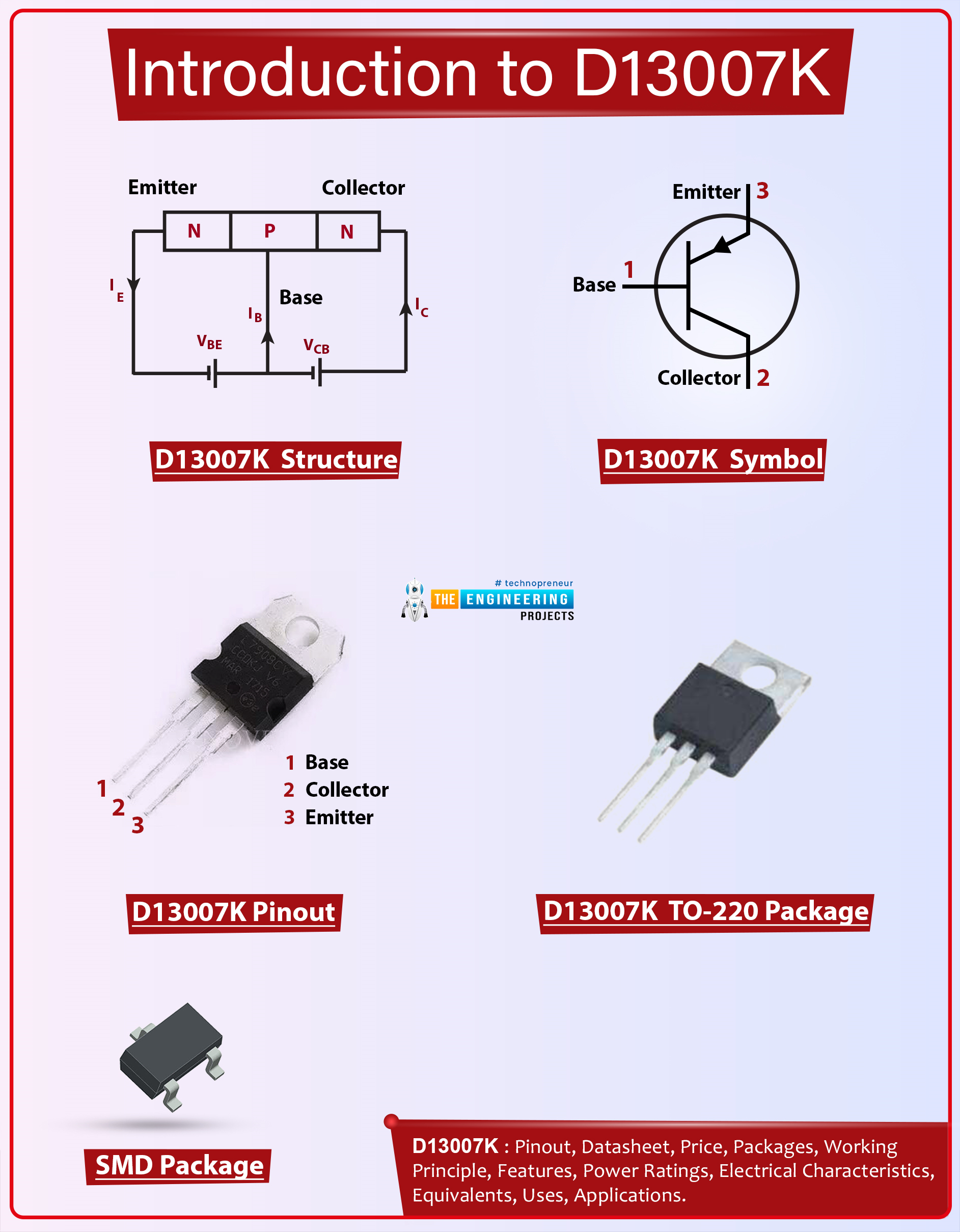
Hello Fellas! Hope you’re well today. Happy to see you around. In this post today, I’ll walk you through the Introduction to D13007K. The D13007K is an NPN power transistor mainly used for switching and amplification purpose. This device is made of silicon material and falls under the category of bipolar junction transistors. As this is an NPN transistor so here major charge carriers are electrons. Holes are major carriers in the case of PNP transistors. This is a high voltage high current capability device used in energy-saving lamps. The collector current of this chip is 8A which means it is best for loads under 8A. And the power dissipation is 80W which projects it is eligible to release 80W power during the operation of this device. The collector-base voltage is 700V and collector-emitter voltage is 400 while the voltage across the base and emitter terminals is 9V which is the voltage needed to start the transistor action and bias the device. Read this entire post till the end as I’ll document the complete Introduction to D13007K covering datasheet, pinout, power ratings, working principle, applications, and physical dimensions. Let’s dive in.

Introduction to D13007K

  • The D13007K is a power transistor that belongs to the NPN transistor family.
  • The three terminals like emitter, base, and collector make this entire device. All these terminals are connected to the external electrical circuit.
  • This is a current-controlled device because the small current at one terminal is employed to handle large current at the remaining terminals.

  • While MOSFETs are voltage-controlled devices and come with terminals like a drain, source, and gate. The gate plays the same role in MOSFETs as what base plays in bipolar junction transistors.
  • The bipolar junction transistors are mainly divided into two types one is PNP transistors and one is NPN transistors.
  • Both electrons and holes play a key role in the conductivity of bipolar junction transistors.
  • But in the case of PNP transistors holes are responsible for the major part of conductivity carried out inside the device while in the case of NPN transistors electrons play a key role in the overall conductivity inside the transistor.
  • PNP transistors are considered less efficient than NPN transistors because electrons are quicker and efficient in the conductivity process compared to holes. The mobility of electrons is far better and quicker than the mobility of holes inside the transistor.

D13007K Datasheet

It is wise to check out the datasheet of the device before incorporating it into your electrical project. The datasheet comes with the main characteristics of the device. Click the link below to download the datasheet of D13007K.

D13007K Pinout

The following figure shows the pinout diagram of D13007K. The D13007K carries three terminals known as: 1: Base 2: Collector 3: Emitter All these terminals carry different doping concentrations. Which leads to the lack of symmetry of this device. The emitter side is highly doped and the collector side is lightly doped. While the collector side is 10-times less doped than the base side.

D13007K Working Principle

  • The transistor working principle is straightforward and simple. It all initiates from the base side. When voltage is applied at the base side, it will bias the device, and as a result, the current will start flowing collector to the emitter terminal.
  • As this is an NPN transistor so here current flow is carried out from the collector to emitter terminals this is the opposite in the case of PNP transistors.
  • When voltage is applied at the base pin in PNP transitory, the current starts flowing from the emitter to the collector terminal.
  • As described earlier this bipolar device is not symmetrical. Which means if you interchange both emitter and collector side then both terminals will start working in reverse active mode and the device will stop working in forward active mode.

D13007K Power Ratings

The following table features the absolute maximum ratings of D13007K.
Absolute Maximum Ratings of D13007K
Pin No. Pin Description Pin Name
1 Collector-emitter voltage 400V
2 Collector-base voltage 700V
3 Base-emitter voltage 9V
4 Collector current 8A
5 Power dissipation 80W
6 Base current 4A
7 Operating and storage junction temperature range -55 to 150C
  • While incorporating this device into your project, make sure the ratings don’t exceed the absolute maximum ratings. Otherwise, it can damage the entire project.
  • The junction temperature and storage temperature ranges from -55 to 150C.
  • The collector-emitter and collector-base voltages are 400V and 700 respectively. And total power dissipation is 80W which demonstrates the amount of power released during the functioning of this device.
  • It is important to note that, don’t apply these ratings more than the required time, else they can affect device reliability.

D13007K Applications

D13007K is used in the following applications.
  • Used in Bistable and Astable multivibrators circuit.
  • Used in voltage regulator circuits.
  • Employed to support loads under 12A.
  • Used in electronic Ballasts.
  • Incorporated in modern electronic circuits.
  • Used in high-frequency power transform.
  • Used in a common power amplifier.
  • Used in energy-saving lights.
  • Used in the high switching power supply.

D13007K Physical Dimensions

The image below represents the physical dimensions of D13007K. By scanning those dimensions you can evaluate the space required for your component in the electrical project. That’s all for today. Thank you for clicking this read and reading it. You are most welcome to share your valuable feedback and suggestions in the section below. They help us produce quality content. You can approach me in the section below if you need any help regarding this article, I’m happy and ready to help you the best way I can. Thank you for reading this post.

Syed Zain Nasir

I am Syed Zain Nasir, the founder of <a href=https://www.TheEngineeringProjects.com/>The Engineering Projects</a> (TEP). I am a programmer since 2009 before that I just search things, make small projects and now I am sharing my knowledge through this platform.I also work as a freelancer and did many projects related to programming and electrical circuitry. <a href=https://plus.google.com/+SyedZainNasir/>My Google Profile+</a>

Share
Published by
Syed Zain Nasir