TDA7294 Power Amplifier Datasheet, Pinout, Features & Applications

Hi Guys! Hope you’re well today. I welcome you on board. In this post today, I’ll walk you through the Introduction to TDA7294. TDA7294 is a monolithic class AB power-based audio amplifier that comes with a DMOS output stage. It is primarily used for the amplification of audio signals in Hi-Fi field applications containing self-powered loudspeakers. The fault protection circuitry used in this device protects against short circuits. 
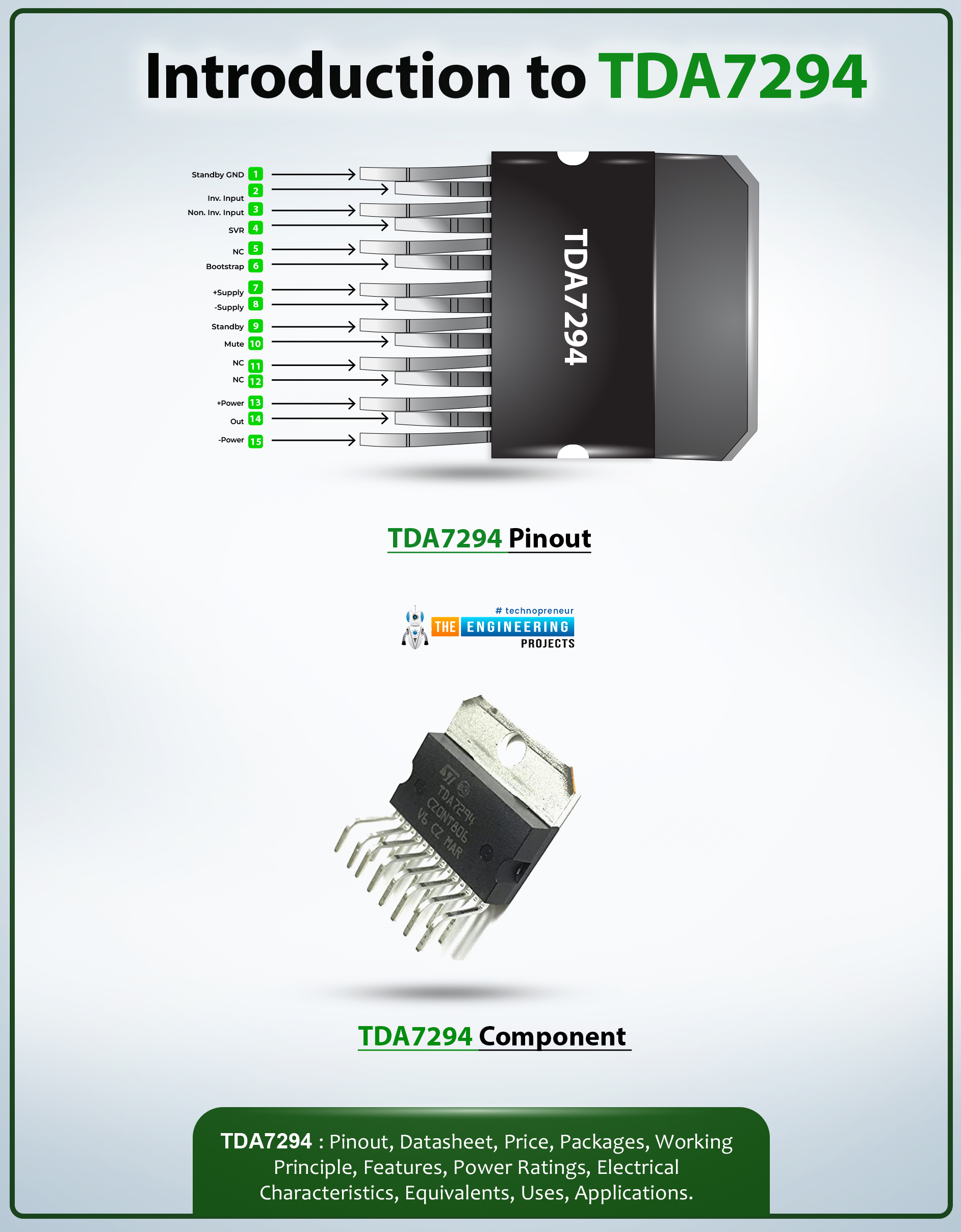
I suggest you read this post all the way through, as I’ll detail the complete introduction to TDA7294 covering datasheet, pinout, features, and applications. Let’s get started.

Introduction to TDA7294

  • TDA7294 is a monolithic class AB power-based audio amplifier that comes with a DMOS output stage.
  • This device comes with a wide voltage supply range and can drive loads of 4V to 8V.

  • This chip comes in multi-watt 15V and 15H packages and offers protection against thermal shutdown.
  • It is widely used in the amplification of audio signals in Hi-Fi field applications.
  • The high-power loudspeakers incorporate this chip for producing the perfect bass sound.
  • You can attach this device with a heat sink and it is capable of generating an output power of around 100 watts.
  • Producing audio signals with high efficiency and high power is the main goal of this amplifier.
  • This chip comes with standby and mute functions with the main aim of removing the noises generated as a result of switching.

TDA7294 Datasheet

Before you incorporate this device into your project, it’s wise to have a look at the datasheet of the component that details the main characteristics of the device. Click the link below to download the datasheet of TDA7294.

TDA7294 Pinout

The following figure shows the pinout diagram of TDA7294.

TDA7294 Pin Description

Hope you’ve got a brief idea about this device. In this section, we’ll cover the pin description of each pin incorporated on the chip.

Pin - 01: Stand-by-GND

This is an output pin that is attached to the ground.

Pin - 02, 03: Inverting input, Non-inverting input

These are the audio amplifier input pins.

Pin - 04: SVR

SVR stands for supply voltage rejection pin that is mainly used to remove the noise from the output signal.

Pin - 05, 11, 12: NC

These are non-connected pins.

Pin - 06: Bootstrap

The bootstrap pin is mainly employed to boost the output swing with a capacitor attached to this pin.

Pin - 07, 08: -, +

We will attach these pins to the positive and negative leads of the voltage supply.

Pin - 09: Stand by

This pin is used to run output in a low current mode.

Pin - 10: Mute

It is mainly employed to disable the output signal.

Pin - 13: 15: -, + Power supply

These pins represent the power supply terminals.

Pin - 14: Out

This is an output pin that offers an amplified audio signal.

TDA7294 Features

The following are the main features of TDA7294.
  • Contains high operating voltage range of +40V to -40V
  • Low distortion and low noise.
  • Comes with a DMOS output stage.
  • The threshold voltage for Standby OFF is 3.5V and standby ON is 1.5V.
  • High power output around 100W.
  • Maximum peak output current = 10A.
  • Features built-in protection circuitry against thermal shutdown and short circuit.
  • Additional functions include mute and stand-by.
  • Open-loop gain = 80dB.

TDA7294 Equivalents

The following are the equivalents to the TDA7294.
  • TDA2030
  • LM386
  • LM3886
  • LM4871
  • TDA2040
  • TDA7293
  • TDA7295
While working with these equivalents, double-check the pinout of these alternatives, as the pinout of these alternatives might differ from the pinout of TDA7294.

TDA7294 Applications

TDA7294 is employed in the following applications:
  • Radio & TV
  • Self-powered loudspeakers
  • Bridge circuits
  • Subwoofers and home stereo systems
That’s all for today. Hope you’ve got a brief insight into the Introduction to TDA7294. If you’re unsure or have any questions, you can approach me in the section below, I’d love to help you the best way I can. Feel free to share your valuable feedback and suggestions around the content we share so we keep coming back with quality content tailored to your exact needs and requirements. Thank you for reading the article.

TDA2030 Audio Amplifier, Datasheet, Pinout, Features & Applications

Hi Folks! I welcome you on board. Happy to see you around. In this post today, I’ll detail the Introduction to TDA2030. This device incorporates a TDA2030 audio amplifier chip that produces 18 W output power with low harmonic distortion.

I suggest you read this post till the end as I’ll walk you through the complete Introduction to TDA2030 covering pinout, datasheet, features, and applications. Let’s get started.

Introduction to TDA2030

  • TDA2030 is a monolithic integrated circuit that comes in a Pentawatt package, mainly used as a low-frequency class AB amplifier.
  • The audio amplifier is a basic circuitry used to amplify the audio signal obtained through a device like a microphone.

  • Audio amplifiers are widely used in scores of applications including Hi-fi devices, Radio wave transmitters, talking toys, Home audio systems, Robots, and as an acoustic weapon for military operation purposes.
  • The main purpose of an amplifier is to convert an electrical signal into an acoustic signal. Any circuit containing an audio signal contains an audio amplifier at the output and the input.
  • The TDA 2030 can generate 14W output power (d = 0.5%) at 14V/4O at ± 14V or 28V, producing output power 8W on an 8O and 12W on a 4O load.
  • This module comes with a wide supply voltage range of up to 36V.
  • It operates on the single or split power supply and protection circuitry against short circuits and offers thermal shutdown.
  • The short circuit protection settings automatically limit the dissipated power, keeping the output transistor operating point within a secure operating range.
  • The TDA2030 offers high output current and carries very low crossover and harmonic distortion.
  • It also features onboard terminal blocks for speakers and an onboard power indicator which indicates the operation of this device when power is provided to this module.
  • This device offers storage and junction temperature ranges of -40 to 150 C.
  • The differential input voltage is +-15V and the output peak current is 3.5A and power dissipation is 20W.

TDA2030 Datasheet

Before you apply this device to your project, it’s wise to scan through the datasheet of the component that highlights the main characteristics of the component. Click the link below and download the datasheet of TDA2030.

TDA2030 Pinout

The following figure shows the pinout diagram of TDA2030.

TDA2030 Features

An audio amplifier is generally developed in such a way that it takes input as the low strength audio signal and as a result, produces the output signal comprising high strength value. The following are the main features of TDA2030.
  • Contains On-board power indicator
  • 18 W mono amplifier circuit design
  • Short-circuit protection to ground
  • Operating Voltage Range = 6 V to 12 V
  • Single or split power supply
  • Main pins are routed to a standard pin header
  • On-board TDA2030A audio amplifier chip
  • Comes with On-board 10K potentiometer for volume adjustment
  • Features On-board terminal blocks for speaker
  • Module Size = 32 x 24 mm
  • Wide-range supply voltage, up to 36 V
  • Thermal shutdown

TDA2030 Applications

The following are the main applications of TDA2030.
  • Used in Hi-fi devices
  • Radio wave transmitter contains an audio amplifier
  • Employed in Talking toys
  • Used in home audio systems and robots
  • An acoustic weapon for military operations

That was all about the Introduction to TDA2030. Hope you find this article helpful. If you have any questions, you can pop your comment in the section below. I’d love to help you the best way I can. Feel free to share your valuable suggestions and feedback around the content we share so we keep producing quality content customized to your exact needs and requirements. Thank you for reading the post.

5 Ways to Make Your Automation Testing More Effective

Hey pals! Welcome to the Engineering Project. We hope you are have a good day. First, we need to understand what automation is, and what its objectives are. Automation is simply the integration of technology to process or run its functions with minimal human intervention or assistance. Its objectives are to improve efficiency, speed and precision of hard or long tasks that are usually performed by humans.  For example, accounting and producing and delivery of products, which were formerly and majorly done by humans. But, in the world of modernity and technology, automation was invented to minimize costs and risks while maximizing profits.  Overall, an open line of communication and good management skills are both critical during the implementation or automation testing services There are significant issues that always need to be addressed, a fragile interrelationship in a sense. For example, testing to check if the system's configurations and processes are working is one of the most overlooked details of IT projects. The sooner defects are found, the less resources are used to fix said defects. It's crucial to ensure the effectiveness of automation. Here is the factor divided into 5 main issues:
  • Knowing What They Want and Need, Take It slow and Start Small.

It's better to take the time and acknowledge what the automation needs and what it needs to do. This is because it's difficult to precisely guess what the requirements, the system design, and how much human interaction it will need while in development as clients usually don't exactly know what they want until they see and use it. So, it's better to start with a small example that can be easily presented to clients. It can then be used as a foundation on what changes or enhancements should be made. 
  • Staffing and Expertise

Having the right staff with proper expertise of the functions you want to have for your automation will make it more effective overall as it will be minimizing risks and upping the chance of both satisfaction and profitability. For example, having a project manager with proper knowledge and experience will be of great help in filling positions required for the automation.
  • Schedule and Test Reports

It is important to have, at the very least, a concrete schedule when it comes to testing the product and when the final release can be expected. At the end of each week, it should focus on summarizing all the progress on the automation that has so far been done; what the changes are, what errors have been crossed and fixed, and the plan on what to do the following week will be.  
  • Automated Testing

All IT projects like automations are encouraged to use Test-Driven Development (TDD) where test cases are simply stated, which are a sequence of steps with an expected outcome or function before starting each step of work. After each phase, testing should not only be done by both dedicated testers, and each member of the team working on the project but also automated test servers which in modern times have been the norm to make test much broader and more frequent.
  • Be open and informative

Make sure that your client monitors the progress of the tests, and catches problems earlier rather than late where costs and risks are higher. Provide proof and suggestions, such as:
  • Live Demos – Instead of Power-point presentations or a detailed text document, provide the client with working examples or software that shows the progress you’ve done.
  • Quality Metrics – In recent years, there have been tools made to generate other types of reports such as those on quality. For example, in Java, the most common programming language for automations, there are many tools that check if there are lines of codes that will lead to errors or bugs, or logic that is too complex, or if code violates standards.
  • Charts – It’s useful to have charts to give both the client and the team a general view of their overall progress. For example, a task board that shows which features haven’t started yet, which are currently in progress, which need to be fixed, and which are done can be useful.  
When there is a major mishap or mismatch, the manager must quickly assess how and what resources are necessary. After each test, requirements may evolve or change, which puts more emphasis on communication and management.

Web Design vs. Web Development

Hi Friends! Welcome to The Engineering Projects. At the present time, it is an important to upgrade the technical skills. As we approach a more digital era, the use of the internet has become part of our day-to-day activities. When it comes to looking up for something online, we always go to our chosen and trusted websites for information. Our trusted website, of course, is pleasing to the eyes, with all the functions and settings working perfectly. Although as a browser, we would sometimes not bother to give a second look at the web design or how it was developed. But if by any chance, your mind seeks to know more, to have in-depth knowledge about websites in general, this article seeks to explain the difference between web design and web development.

Web Design and Web Development: Which Is Which?

Web Design

In layman’s terms, web design involves the aesthetic of a particular website. It is how the site looks from an outsider’s point of view. The web designer’s job includes making the website look aesthetically-pleasing to its viewers—these would include a selection of the color scheme to be used, selection of the font and font size, and where the website functions should be placed.  Web design mainly requires the artistic and creative touch of the web designer. Aside from the aesthetic look of a website, there are numerous areas in web design that the web designer should never neglect, including the user interface design (UI), the graphic design, user experience design (UX), and search engine optimization (SEO). To make web design possible, web designers use a bunch of tools that would be perfect for the production process that they would be needing. Web designers normally would use vector and raster graphics editor in order to make design prototypes or web-formatted images. The tools that they use are updated from time to time in order to always have an updated software or standards. Web designers also use technologies to create websites like CSS and HTML. The UI and UX of a website are also considered in the web design. The UX pertains to the layout, including labeling and clear instructions on each function. UI, however, is the more commonly used function of a website, as this pertains to the website’s interface as a whole.

Web Development

As the back end (and front end) of a website, web application development services consist of all the software and programs that are needed in making the website thoroughly and smoothly functioning. A web developer’s main objective is to develop the backend of a website to give a pleasing and smooth web experience for whoever will browse the website. Since web development is a complicated and tedious task, it requires a skilled and skilled web developer, who is also familiar with technical computer languages such as Java, ASP, Coldfusion, and PHP, among others. Web development can be as simple as making a single static page or even making web-based applications of the internet and web apps. Web developers have numerous tasks to accomplish when developing a website. These include web engineering, web content development, client-side or server-side scripting, web server, network security configuration, e-commerce development, and even web design. Web development sometimes uses content management systems (CMS) in order to make the necessary changes in the content easier and more accessible with basic technical skills.  Web Design vs. Web Development: Brief Summary Both web development and web design are important in making a website. These two approaches (front end and back end) when combined, produce, and develop the system and design needed for a completely working and aesthetically-pleasing website. Web development mostly pertains to the back end of a website, making sure that all the systems, functions, and configuration are working properly. This may be unseen by the web browser but can surely experience it upon browsing any given website. The website’s aesthetic look and design, however, is part of the work of a web designer. As a skilled web designer, the graphics, colors, fonts, graphics placement, UI and UX, and features placement are included in the whole web design. Web design and web development work hand-in-hand. You cannot develop a website with just a web design, just as you cannot make your design work with just the web design.

Introduction to Arduino MKR GSM 1400

Hello Guys! I welcome you on board. Happy to see you around. In this post today, I’ll walk you through the Introduction to Arduino MKR GSM 1400. The Arduino MKR GSM 1400 is a microcontroller board that is based on the SAMD21 microcontroller. This device connects with a cellular network for developing communication. This GSM board is a one-stop solution for developing your sensor network or you can use it as a device sending a text message about the occurring of certain events remotely. A module from u-blox, the SARA-U201 (which is a power chipset that activates using multiple cellular range bands) is responsible for GSM / 3G connectivity inside the device. I recommend you read this post till the end as I’ll detail the complete Introduction to Arduino MKR GSM 1400 covering pinout, pin description, features, programming, and applications. Let’s get started.

Introduction to Arduino MKR GSM 1400

  • The Arduino MKR GSM 1400 is a microcontroller board that is based on the SAMD21 Cortex®-M0+ 32bit low power ARM microcontroller.
  • This device is mainly introduced for laying out the communication with cellular networks.
  • Connecting Arduino with the GSM network is as easy as the program used for LED blinking. With this device, you can send or receive calls or messages and approach the different types of servers for exchanging data.
  • The module comes with 8 digital I/O pins while the number of analog pins are 7 and the pins used as PWM pins are 13.
  • The board supports UART serial communication protocol. Other communication protocols include SPI and I2C communication protocol.
  • The USB port is incorporated in the device which is used for sending the number of instructions from the computer using Arduino IDE software.
  • The internal flash memory is 256KB and the SRAM is 32KB. There is no EEPROM present inside the device. The Arduino program (sketch) is stored in the flash memory while SRAM is responsible for producing and manipulating variables when it runs.
  • The clock frequency is 32.768 kHz (RTC), 48 MHz… which is responsible for the synchronization of all internal functions.

Arduino MKR GSM 1400 Pinout

The following figure represents the pinout diagram of Arduino MKR GSM 1400.

Arduino MKR GSM 1400 Pin Description

Hope you’ve got a brief overview of this GSM device. In this section, we’ll detail the pin description of each pin available on the device. Let’s get started.

Analog Pins

There are 7 analog pins available on the board. These pins can receive any number of value in opposed to digital pins that receive only two values HIGH and LOW.

Digital Pins

There are 8 digital pins incorporated on the board which you can use as an input or output based on the requirement. These pins get two values HIGH or LOW. When the pins receive 5V they are in a HIGH state and when these pins receive 0V, they are in a LOW state.

PWM Pins

There are 13 PWM pins on the board. These pins produce analog results through digital means.

SPI Pins

The board supports SPI (serial peripheral interface) communication protocol that ensures the communication between controllers and other peripheral devices like shift registers or sensors. It contains two pins… MISO (master input slave output) and MOSI (master output slave input) are used for SPI communication.

UART

The board comes with a UART communication protocol that guarantees serial communication and comes with two pins Rx and Tx. The Rx is a receiving pin that receives the serial data and Tx is the transmission pin that is used to transmit the serial data.

Arduino MKR GSM 1400 Features

The following are the main features of Arduino MKR GSM 1400.
  • Microcontroller = SAMD21
  • Secure Element = ATECC508
  • Radio module = u-blox SARA-U201
  • Supported Battery = Li-Po Single Cell, 3.7V, 2500mAh Minimum
  • Digital I/O Pins = 8
  • Analog Pins = 7
  • PWM Pins = 13
  • Flash Memory = 256KB
  • SRAM = 32KB
  • EEPROM = no
  • Circuit Operating Voltage = 3.3V
  • Power Supply (USB/VIN) = 5V
  • External Interrupts = 10
  • DC Current per I/O Pin = 7 mA
  • SPI = 1
  • UART = 1
  • I2C = 1
  • SIM Card = MicroSIM (not included with the board)
  • Working region = Global
  • Carrier frequency = GSM 850 MHz, E-GSM 1900 MHz, DCS 1800 MHz, PCS 1900 MHz
  • Clock Speed = 32.768 kHz (RTC), 48 MHz
  • Full-Speed USB Device and embedded Host = 1
  • LED_BUILTIN = 6
  • Size = 25x67mm
  • Weight = 32gr.

Programming

  • This GSM board is programmed by Arduino IDE software which is specifically introduced by Arduino.cc to program the Arduino boards.
  • The software comes with an LED blinking program which you can use to test the board if it’s operating properly.
  • Connect your board with the computer using a USB cable and start playing with it. You can send the number of instructions to the board from the computer using Arduino IDE software.
  • The board comes with a built-in Bootloader that is used to burn the program inside the microcontroller board. You don’t require an external burner to burn the program in the controller.

Arduino MKR GSM 1400 Applications

This device is mainly used in GSM cellular projects. The following are the main applications of Arduino MKR GSM 1400.
  • Used in tracking projects
  • Used in home automation
  • Employed in GSM home alarm
  • Employed in fire forest monitoring and detection
  • Used to send messages to control LED color
  • Used in 2-factor authentication for ATM project
That’s was all about the Introduction to Arduino MKR GSM 1400. If you’ve any questions, you can pop your comment in the section below. I’d love to help you the best way I can. You’re most welcome to share your valuable suggestions and feedback around the content we share so we keep coming back with quality content customized to your exact needs and requirements. Thank you for reading the article.

Master Slave JK Flip Flops in Proteus ISIS

Hey pals! I wish you are doing great. Welcome to a new lesson about the Digital Logic Circuits in The Engineering Projects. In the past tutorials, we Designed the Basic JK Flip Flop. Today, we'll talk about the following Points:
  1. What are JK Flip Flops?
  2. What are the Master Slave Flip Flops?
  3. How does the Circuit of Master Slave Flip Flop looks?
  4. How types of JK Flip Flop different from each other?
  5. How does the simulation of Master JK Flip Flip take place in Proteus ISIS?
Moreover, we'll also learn some key concepts in DID YOU KNOW portions. Yet Let's recall some points about the topic.  Flip Flops are the building block of a huge number of electronic systems and devices. A Flip Flop is a Digital circuit that can take the bits as input, work with the bits, Store the bits and can output the bits. it has four basic types and at the moment we are discussing the JK Flip Flops.

DID YOU KNOW????????????

The basic JK Flip Flops face a condition where when both the Inputs are HIGH and the Clock remains HIGH for a long time, then the output of JK Flip Flop becomes uncertain and this situation is called Race around Condition in JK Flip Flops..

JK Flip Flops

As discussed in the Previous tutorial , we define the JK Flip Flops as:
"The JK Flip Flops are the Modification of Set-Reset Flip Flops that contain two outputs and are able to work with the Invalid Condition of Flip Flops."
There are mainly two types of JK Flip Flops:
  1. Basic JK Flip Flops
  2. Master Slave JK Flip Flops.
The main focus of this tutorial is Master JK Flip Flops so lets find what are they.

Master Slave JK Flip Flops

The Master Slave JK Flip Flops are considered better than Basic JK Flop and we define them as:
"Master Slave JK Flip Flop is two input two output sequential Logic Circuits that are the Combination of two Basic JK Flip Flops and  work well even in Race around Condition of JK Flip Flops."
In Master Slave JK Flip Flops there are two JK Flip Flops that are connected in series. The 1st JK Flip flop is called the "Master" circuit and the other is called the "Slave" circuit. The output of the Master Circuit is connected with the inputs of Slave circuits. At the same token, the output from the Slave Circuit are then fed into the input terminals of Master Circuit. The circuit also contain an Invertor that is Connected with the clock and slave circuit in such a way that the Slave circuit always contain the inverting clock signal as the master circuit. Hence when Master circuit get the clock HIGH, then the slave circuit get the LOW and vise Versa.

Difference of Basic JK Flip Flop and Master Slave JK Flip Flop

Both of the circuits belongs to the same family but they are different in many ways:
  1. Basic JK Flip Flop contain only one circuit but Master Slave JK Flip Flop contains two.
  2. The Basic JK Flip Flop have the Race around condition but Master Slave does not.
  3. Basic JK Flip Flop is less complex than Master Slave JK Flip Flop.
  4. Basic JK Flip Flop is less used than Master Slave JK Flip Flop.
  5. Basic JK Flip Flop does not require any NOT Gate but Master JK Flip Flop use it.

Circuit of Master Slave JK Flip Flop

If we talk about the Circuit of the JK Flip Flop then it is always convenient to use the IC presented in Proteus ISIS. We'll show you the Circuit of Master Slave through ISIS but for the best concept and the working of the Circuit, we'll demonstrate the Logic Gate Circuit of Master Slave JK Flip Flop during the Simulation. Let's have a look at the circuit of Master Slave JK Flip Flop with IC:

DID YOU KNOW???????????

When the condition of Master Slave Flip Flop is J=1 and K=1 then the values at Q  and Q' remains change according to the flow of clock.

Working Mechanism of JK Flip Flops

It is important to understand how Master Slave Flip Flop works. When the clock Pulse is set to be high, the circuit of Slave is isolated. The Slave circuit remains isolated until the Clock is high. At this position, the J and K have an effect at the output of the whole circuit. When we set the J as LOW and as HIGH. The output of Switch 4 (Look at the picture below) will goes to the 2nd Input of switch 6. In this Condition, the Slave circuit copies the Master circuit. Similarly, when you change the values of J and K then you will Get different outputs according to the condition of clock.

Simulation od Master Slave JK Flip Flop in Proteus ISIS

Fire up your Proteus Software.

Material Required

  1. Three input NAND Gate
  2. Two input NAND Gate
  3. Logic Toggle
  4. LED-RED
  5. Ground Terminal
  6. Connecting Wires
  • Click the 'P" button and write NAND Gates, Logic Toggle, LED in the pop up window one after the other.
  • Arrange 2 three input NAND Gates at the Working area vertically.
  • Get 6 two input NAND Gate just according to the image given below:
  • Set three Logic Toggles vertically, at the start of Three input NAND Gates.
  • For the output device, use the Led and set them just after the last two NAND gates.
  • Go to Ground Terminal from the side of Proteus screen and choose Ground Terminal.
  • Set the Ground terminal just after the LEDs.
  • Place the NOT Gate just below the Three inputs NAND Gates.
  • Connect the whole system through wires as reported by the following picture:
NOTE: You can also use the CLOCK instead of the Logic toggles in the experiment but this was not suitable for the demonstration purpose for me.
  • Change the values of the toggle J,K and CLK one after the other to check the outputs.
This is the required circuit. Truss today we saw what are the Flip Flops, what are the JK Flip Flops. We saw the types of JK Flip Flops and leaned how can we perform the Practical simulation of Master Slave JK Flip Flops.

JK Flip Flop Circuit Diagram in Proteus

Hello Learner! I hope you are doing great. Welcome to another tutorial at The Engineering Projects. This blog is the part of series we have stated about the Digital Logic Circuits. Previous to this, we learned Implementation of SK Flip Flops in Proteus. at the present day, we'll seek the knowledge about the following points:
  1. What are Flip Flops?
  2. What are JK Flip Flops?
  3. How can we record the Truth Table of JK Flip Flops?
  4. What is the Procedure to Construct the circuit of JK Flip Flop through Logic Gates and IC circuit?
Moreover, we'll also have some useful bits of Information in Did you know Sections. Let' see the explanation of the concepts given above.

Flip Flops

The Flip Flops are the building blocks of many of  the Electronic Circuits. We define the Flip Flops as:
"The Flip Flops are the type of sequential Logic Circuits that are mainly made through the Logic Circuits and have the ability to receive, store, and show the output in the form of binary bits i.e, 1 and 0."
There are mainly four types of Flip Flops:
  1. SR Flip Flops
  2. JK Flip Flops
  3. D Flip Flops
  4. T Flip Flops
The main focus of this blog is JK Flip Flop so we'll discuss them in detail.

JK Flip Flops

JK flip Flops are the sequential Circuits and are the very much similar to SR Flip Flops. We introduce the JK Flip Flips as:
"The JK Flip Flops are the Universal Flip Flops containing two inputs, two outputs and a Clock in the Circuit. They have e the ability to avoid the invalid or Illegal condition of the Flip Flops."
The name of the inputs are said to be J and K respectively. Unlike SR Flip Flops ( where S stands for Set and R stands for Reset) the inputs of JK Flip Flops are titled autonomously. Somehow, related to the inventor of the JK Flip Flop "Jack Kilby".

DID YO KNOW???????????

JK Flip Flops are useful in many ways as: They have Low power dissipation. They are much Faster than their sibling Flip Flops.
]The output of the JK Flip Flops are named as Q and Q'. As the name implies , both the Outputs are opposite to each other. When Q is HIGH , the Q' is Low and same is the case with the opposite condition. The Truth Table Of JK Flip Flop is given next:
CLOCK J K Q Q’
High 0 0 Unchanged Unchanged
Low Unchanged Unchanged
High 0 1 0 1
Low 0 1
High 1 0 1 0
Low 1 0
Low 1 1 1 0
High 0 1
There are two types of JK Flip Flop named as:
  1. Basic JK Flip Flop.
  2. Master-Slave JK Flip Flop.
Yet in this lesson, we'll make a clear idea about the Basic JK Flip Flop only. For best concepts, we'll not just observe the Circuit diagram of JK Flip Flop but we'll Construct a Circuit using different tools and Components in Proteus ISIS. We'll learn about the Formation of JK Flip Flop in two ways:
  1. JK Flip Flop through Logic Gates.
  2. JK Flip Flops through IC.
Rush toward your Proteus Software and learn how can you make this in just simple steps.

DID YOU KNOW????????????

The JK Flip Flops are the better version of SR Flip Flops and are better than those just using a NOR Gate.

JK Flip Flop Circuit Diagram in Proteus

  • Start your Proteus Software.
  • Get the following material from the Pick Library through "P" button..

Material Required

  1. 3 input NAND Gate.
  2. 2input NAND Gate.
  3. Logic Toggle.
  4. LED-RED.
  5. Ground Terminal.
  6. Connecting Wires.
  • Get the first three elements from the Pick Library one by one.
  • Select two 3 input NAND Gates and arrange them vertically at the working area one after the other.
  • Repeat the same step for Two input NAND Gates just after the two gates set before.
  • Get two Logic Toggles and arrange them just before the Gate 1 and 2.
  • Take two LEDs and place them just after switch 3 and 4.
  • Get a Clock and set it in between two logic Toggles.
  • JK Flip Flop Circuit Diagram in Proteus is shown in image given below:
  • Pop the Play button to start simulation.
  • Change the values of the inputs and observe the output at each gate. You will get the following table:
CLOCK J K 1 2 Q Q’
High 0 0 Unchanged Unchanged Unchanged Unchanged
Low Unchanged Unchanged Unchanged Unchanged
High 0 1 1 1 0 1
Low 1 1 0 1
High 1 0 1 1 1 0
Low 1 1 1 0
Low 1 1 1 1 1 0
High 1 1 0 1
Hence this is the required output.

JK Flip Flop IC (Integrated Circuit)

Due to the usability of JK Flip Flop, Proteus ISIS has added many JK Flip Flop IC. In this way, we do not need to design all the circuit. Instead we can simple using JK Flip Flop IC.Let's see how it will work:

Material Required

  1. JK Flip Flop ( IC)
  2. Logic Toggle
  3. LED-red
  4. Ground Terminal
  • Place the JK Flip Flop IC at the working area.
  • Connect Logic Toggles and clock at the respective ports.
  • Add the Led at Q and Q' ports.
  • Ground the LED's through Ground Terminals.
  • Change the values of the Logic Toggles again and again and check that does you get the required output or not.

Easily available JK Flip Flop IC

Proteus also contain many other ICs of JK Flip Flop. Some of them are as follows:
  1. 74LS107 that contain a Dual JK Flip Flop with CLEAR.
  2. 4027B is an IC that is Dual JK Flip Flop.
  3. 74LS73 contains Dual JK Flip Flop with CLEAR.
  4. 74LS76 has Dual Flip Flop with PRESENT and CLEAR.
Truss, Today we recalled that what are the Flip Flops, what are its types, learned a great information about JK Flip Flops and designed its circuit in Proteus ISIS in two ways. Hopefully, you got the required pieces of particulars. in the next Lesson, we'll talk about the Master slave JK Flip Flops.
Syed Zain Nasir

I am Syed Zain Nasir, the founder of <a href=https://www.TheEngineeringProjects.com/>The Engineering Projects</a> (TEP). I am a programmer since 2009 before that I just search things, make small projects and now I am sharing my knowledge through this platform.I also work as a freelancer and did many projects related to programming and electrical circuitry. <a href=https://plus.google.com/+SyedZainNasir/>My Google Profile+</a>

Share
Published by
Syed Zain Nasir