D-Type Flip Flop Circuit Diagrams in Proteus

Hey Mentees! Welcome from the team of The Engineering Projects. We hope You are having a reproductive day. To add more reproduction, let's learn another Logical Circuit from scratch. In this Tutorial, we'll grasp the following topics:
  1. What are D-Type Flip Flop?
  2. Which is the IC of D Flip Flop in Proteus ISIS?
  3. How is the working of D Flip Flop?
  4. How can we design the Truth Table of D Flip Flop?
  5. How can we Perform the formation of D Flip Flops in Proteus ISIS?
Moreover, we'll have small chunks of information in DID YOU KNOW Sections. At this instance, Let's start the learning.

D-Type Flip Flops

D-Type Flip Flops are important Logical Circuits and we Introduce it as:
"The D-Type Flip Flop is a type of Flip Flop that captures the value of D input for a specific time of the Clock edge and show the output according to the value of D at that time."
D-Type Flip Flops have the ability to Latch or delay the DATA inputs and therefore are the improved version of the SR Flip Flop (In which the data shows the Invalid output when the inputs are HIGH) . Recall that Flip Flops are the Logical Circuits that can hold and store the data in the form of bits and are important building blocks of many of electronic devices and circuits.
DID YOU KNOW???????????????????????? The D Flip Flop is also known as the Data Flip Flop.
When we observe the circuit of D Flip Flop we observe 2 Important points in the D flip Flops:
  1. The D Flip Flop is the circuit of active High SR Flip Flop that have the S and R inputs connected together with an invertor gate so that both S  and R (looking with the point of view of SR Flip Flop) will always have the opposite state to each other.
  2. The circuit has only one input called D input and it always has a clock that has one of the major effect at the output of D Flip Flop.

D Flip Flop IC

IC's play a magical role in the world of electronics. They make the circuit so simple and decrease the chances of the errors in the circuit. for D Flip Flop, the IC Used has a number CD4013 and for better understanding, D Flip Flop IC named 4013 is shown in the Proteus software in the image below: The S and R are the additional pins to use it for the higher level Experiments. Yet for the simplicity and core information, we'll use Logic Gates when we'll perform in the practical section.

Working of D Flip Flop

In the working of D type Flip Flop, we observe that the D is the only input of the D Flip Flop. yet, the Clock also has the effect in the output of the circuit. Due to the Latched Circuit of Flip Flops, all this discussion would be pointless if we took the concept in the mind that at every pulse, the data of the Flip Flop is changed. Truss, we use an Enabler or Clock in the Circuit through which we can separate the circuit from the input at the instance of our will. When clock is HIGH: Thus, when the D is set HIGH the circuit is said to be in the "Set" State. By the same token, when the D input is LOW the circuit is said to be in the "Reset" position. Unlike SR Flip Flop, the output Q is same as the value of D input and Q' is the vise versa. When Clock is LOW: During the operation when the Clock or Enable input is LOW, any value at the D does not have any effect on the circuit's output. This position is called the "Don't Care" State of D Flip Flop.

Truth Table of D Flip Flop

Based upon the Concepts given above, one can easily design the Truth Table of the D Flip Flop. Let's have a look at the Truth Table.
Inputs Output
CLK D Q Q’
0 X No Change
1 0 0 1
1 1 1 0
For the purpose of best understanding, we are going to check these concepts and the circuit information in the simulation Software. We are using the Proteus ISIS here.

Performance of D Flip Flop i Proteus ISIS

To perform the experiment in the software, just follow the simple steps given next.

Material Required

  1. NAND Gate
  2. NOT Gate
  3. Logic Toggle
  4. LED-RED
  5. Ground Terminal
  6. Connecting wires
  • Fire up your Proteus ISIS.
  • Pop the "P" button present at the screen and Write the name of 1st four devices and select them one after the other.
  • Arrange four NAND gates and the inverter gate (NOT Gate) at the working area just according to the image given below:
  • Take Logic Toggles and arrange them just at the left side of the system.
  • Get the LED's for the output and connect one of them with the output of switch Q and Q'.
  • Go to Terminal mode>Ground, attach the one ground Terminal with each the LEDs.
  • Connect all the devices according to the diagram given next:
  • Change the value of the Clock and observe does the value of the output change?
  • Turning the LED on means the output is HIGH and vise versa.
  • For convenience, the D Flip Flop can also be obtained by using a NAND as NOT in the Circuit as shown in figure:

DID YOU KNOW?????????????

In real life, the Clock is used in the place of Logic Gate (as shown in the image above) because it automatically changes the direction and change the output of the D Flip Flop. 
NOTE: You can also use the Logic Probe instead of the Grounded LED. Truss, in this session, we saw what are the D Flip Flops, how does they work, how an we design the Truth Table of D Flip Flop and how can we perform it practically in Proteus ISIS. In the next session, we'll know what are T Flip Flop and how is its Simulation in Proteus ISIS.

74LS76 Dual JK Flip-Flop Datasheet, Pinout, Features & Applications

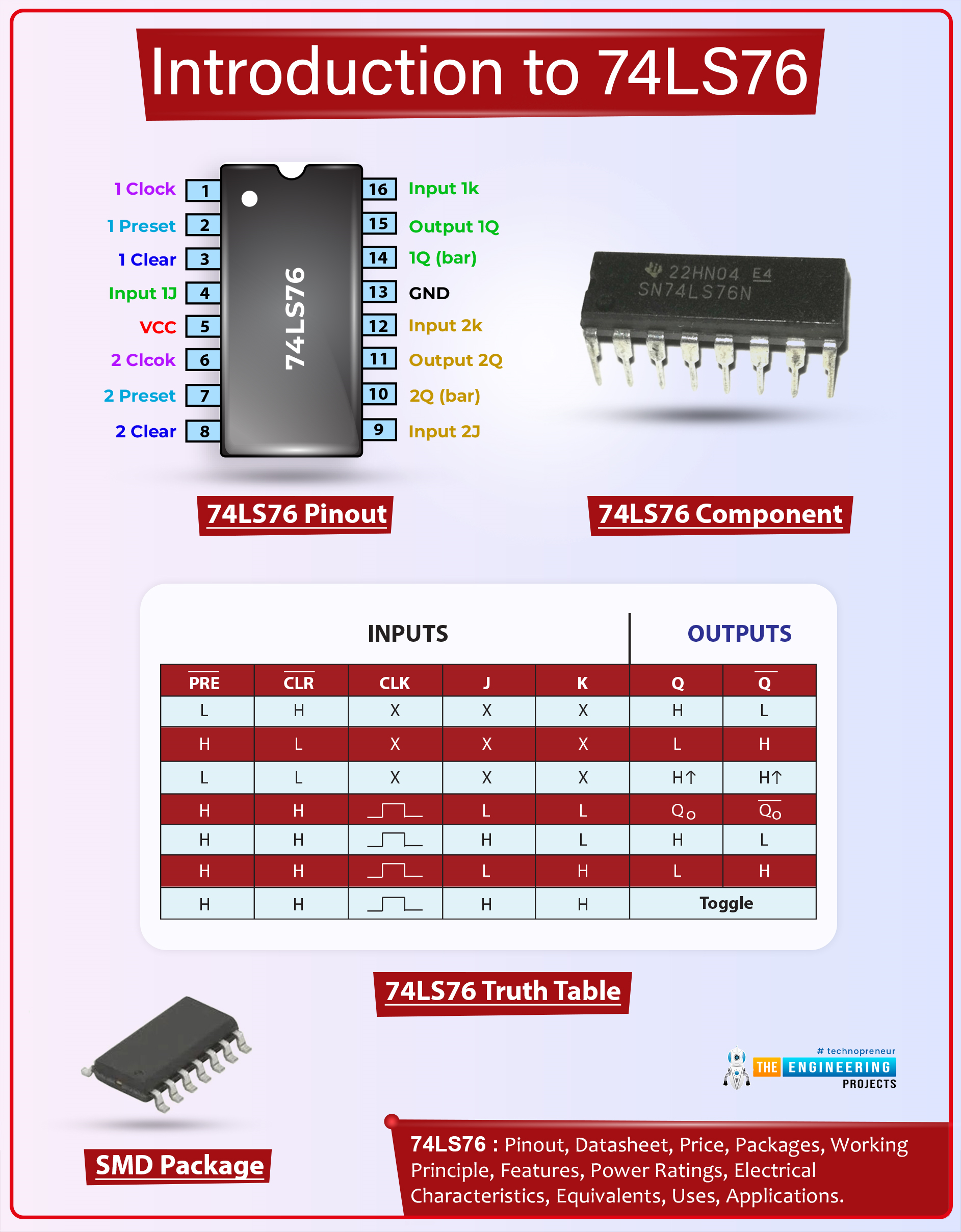
Hi Folks! Hope you’re well today. Happy to see you around. Today, I’ll walk you through the Introduction to 74LS76.

The 74LS76 comes with separate J, K, clock pulse, direct clear inputs, and direct set. These flip-flops are developed in such a way when the clock is set HIGH, data will be received enabling inputs.

I suggest you buckle up as I’ll detail the complete Introduction to 74LS76 covering datasheet, pinout, features, alternatives, and applications.

Introduction to 74LS76

  • The 74LS76 comes with separate J, K, clock pulse, direct clear inputs, and direct set. These flip-flops are developed in such a way when the clock is set HIGH, data will be received enabling inputs.
  • This IC contains two JK flip-flops and each flip-flop can be utilized individually for the required applications.

  • These flip-flops are mainly employed in control registers, shift registers, and storage registers and are termed as latching devices due to their ability to remember every single bit of data.
  • These devices latch the output based on the stored binary data.
  • It is important to note more than one flip-flop can be combined in series for storing a small amount of data as an EEPROM.
  • The operating voltage range of this dual JK flip-flop is 2V to 6V and comes in 14-pin PDIP, GDIP and PDSO packages.
  • This JK flip-flop is termed the best pick for practical applications as it possesses stable output for all types of inputs.
  • The J and K inputs logic levels will be performed as per the Truth Table as long as minimum set-up times are taken into observation.
  • Know that the Input data is converted to the outputs when the HIGH-to-LOW clock transition occurs.
  • This IC houses two JK flip-flops and is powered by +5V.

74LS76 Datasheet

Before you apply this component to your electrical project, it’s wise to scan through the datasheet of the component that highlights the main characteristics of the chip. Click the link below to download the datasheet of 74LS76

74LS76 Pinout

The following is the pinout diagram of 74LS76. The following table represents the pin description of each pin integrated on the chip.
Pin Description of 74LS76 Dual JK Flip-Flop
Pin No. Pin Description Pin Name
1,6 These pins should be provided with a clock pulse for the flip flop Clock-1/ Clock-2
2,7 Preset input pins drive Flip Flop to a set state. Preset-1 / Preset-2
16,12 Input pin of the Flip Flop 1K/ 2K
4,9 Another Input pin of the Flip Flop 1J / 2J
14,10 The inverted output pin of Flip Flop 1Q(bar) / 2Q (bar)
15,11 Output Pin of the Flip Flop 1Q / 2Q
3,8 Clear input pin drives Flip Flop to a reset state. 1 CLR (bar)/ 2 CLR (bar)
13 Connected to the ground Ground
5 Powers the IC with 5V Power (+Vs)

74LS76 Truth Table

The clear and preset are termed as the asynchronous active-low inputs. When they are set LOW, they result in overriding the J-K and clock inputs allow the output to remain in the steady-state levels. The truth table of 74LS76 is shown below.

74LS76 Features

The main features of the chip are described below.
  • Operating Voltage Range = 2V to 6V
  • Low-Level Output Voltage Max. = 0.25V
  • High-Level Output Voltage Min. = 3.5 V
  • Dual JK Flip Flop Chip
  • Operating Temperature Range = -55 to -125°C
  • Low-Level Input Voltage Max. = 0.8 V
  • High-Level Input Voltage Min. = 2 V
  • Available Packages = 14-pin PDIP, GDIP, PDSO

74LS76 Applications

The following are the main applications of flip-flop 74LS76.
  • Employed in Memory/Control Registers
  • Used in Shift Registers
  • Used in Latching devices
  • Incorporated in EEPROM circuits

That’s all for today. Hope you’ve got a clear insight into the Introduction to 74LS76. If you have any questions, you can pop your comment in the section below, I’d love to help you the best way I can. Feel free to share your valuable feedback and suggestions around the content we share so we keep producing quality content tailored to your exact needs and requirements. Thank you for reading the article.

CD4011 NAND Gate Datasheet, Pinout, Features & Applications

Hi Guys! Hope you’re well today. I welcome you on board. In this post today, I’ll detail the Introduction to CD4035.

CD4011 IC belongs to the CD40xx CMOS IC series. The CD4011 chip comes with four independent NAND gates. This device is used to perform the Boolean function Y = A × B or Y = A + B in positive logic. This IC is widely used in many applications including Portable Audio Docks, AV Receivers, and Blu-Ray Players.

I suggest you read this entire post till the end as I’ll walk you through the complete introduction to CD4011 covering datasheet, pinout, features, truth table, alternatives, and applications. Let’s jump right in.

Introduction to CD4011

  • CD4011 IC belongs to the CD40xx CMOS IC series. The CD4011 chip comes with four independent NAND gates.
  • It is important to note that the output voltage and the operating voltage of this IC are equal.

  • This chip is widely used in many electrical circuits including mp3 players, AV receivers, Blu-ray players, and home theater.
  • If you want to use this chip as a logic inverter, you can reconfigure the NAND gates into NOT gates.
  • Less transition time makes this device the best pick for high-speed applications.
  • The typical operating voltage of this device is 5V which comes in 14-pin PDIP, GDIP and PDSO packages.
  • The operating voltage range is -55 to 125C and the propagation delay time is 60ns.

CD4011 Datasheet

Before you incorporate this component into your electrical project, it’s better to scan through the datasheet of the component that comes with the main characteristics of the device. You can download the datasheet of CD4011 by clicking the link below.

CD4011 Pinout

The following figure shows the pinout diagram of CD4011. The following table represents the pin description of each pin available on the chip.
Pin Description of CD4011
Pin No. Pin Description Pin Name
1,2,5,6,8,9,12,13 First Input pin of the NAND gate NAND Gate Input pins
3,4,10,11 The Inverting input pin of the Op-Amp A NAND Gate Output pins
14 5V is used to power the IC Vcc (Vdd)
4 Connect to the ground Ground Vss

CD4011 Features

The following are the main features of CD4011.
  • Typical Operating Voltage = 5V
  • Operating Temperature Range = - 55 C to + 125 C
  • Low-Level Output Current = 1.5mA
  • High-Level Output Current = - 1.5 mA
  • Propagation Delay Time = 60 ns
  • Dual Input NAND Gate – Quad Package
  • Available Packages = 14-pin PDIP, GDIP, PDSO

CD4011 Truth Table

The following figure shows the truth table of CD4011. You can see from the truth table that the output of the device will only be LOW when both inputs of the device are HIGH, in other cases, it will be HIGH.

CD4011 Circuit Diagram

The CD4011 circuit diagram is shown in the figure below. You can see from the image above that this IC comes with four independent NAND gates. It carries 12 input-output pins available for four NAND gates. Power up the IC with VCC and Ground pins. The operating voltage of this device is 5V but it can also work at 7V.

CD4011 Equivalents

The following are the alternative to CD4011.
  • SN54LS00
  • SN74HC00
Before incorporating these alternatives into your project, double-check the pinout of the alternatives as the pinout of the CD4011 might differ from the pinout of the equivalents.

CD4011 Applications

The CD4011 chip is used in the following applications.
  • Employed in portable Audio Docks
  • Used in AV Receivers
  • Used in MP3 Players or Recorders
  • Applied in Home Theater
  • Incorporated in Blu-Ray Players
  • Employed in Personal Digital Assistants (PDAs)

That’s all for today. Hope you’ve got a brief insight into the Introduction to CD4011. If you have any questions, you can pop your comment in the section below. I’d love to help you the best way I can. You’re most welcome to share your feedback around the content we share so we keep sharing quality content tailored to your exact needs and requirements. Thank you for reading the post.

BSS123 N-Channel MOSFET Datasheet, Pinout, Features & Applications

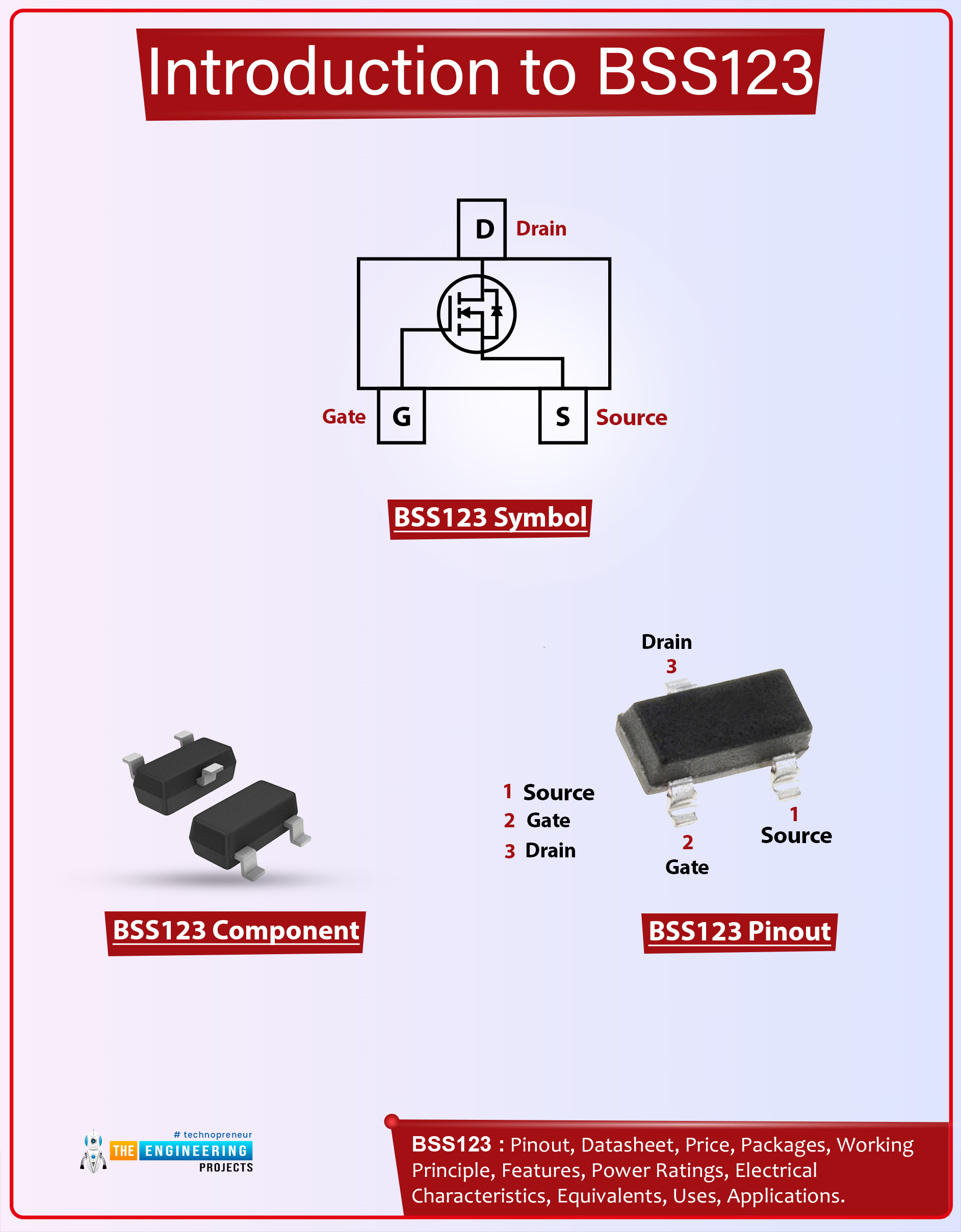
Hi Guys! Hope you’re well today. Happy to see you around. In this post today, I’ll walk you through the Introduction to BSS123.

The BSS123 is an N-Channel Logic Level Enhancement Mode Field Effect Transistor that comes in surface mount package SOT-23. It is a rugged and reliable device that comes with a drain-source voltage of around 100V while the gate-source voltage is -+20V. It is mainly used in low voltage and low current applications like servo motor control and switching and amplification applications.

I suggest you buckle up as I’ll detail the complete Introduction to BSS123 covering datasheet, pinout, features, and applications. Let’s get started.

Introduction to BSS123

  • The BSS123 is an N-Channel Logic Level Enhancement Mode Field Effect Transistor that comes in surface mount package SOT-23.
  • This field-effect transistor is widely used in amplification and switching applications in a range of electronic devices.
  • This is a three-terminal device with terminals named: gate, source, and drain. Sometimes, the body part is also considered as terminal, making it a four-terminal device.

  • The drain current of this component is 170mA and it comes with a low threshold voltage of 1.7V.
  • Know that the gate terminal is electrically insulated since it carries no current and is commonly called as Insulated Gate FET (IG-FET).
  • There are two types of MOSFET i.e. N-channel MOSFET and P-channel MOSFET. This BSS123 chip falls under the category of N-channel MOSFET where electrons are the major charge carriers. In P-channel MOSFETs, holes are the major carrier.
  • The movement of electrons is better than the movement of holes, so N-channel MOSFETs are better than P-channel MOSFETs and possess less resistance. The reason… with high loads the N-channel MOSFETs remain cool while P-channel MOSFET goes hot in the presence of high loads.
  • The charge carriers (electrons in this case of N-channel MOSFET) enter the channel through the source terminal and leave the channel through the drain terminal.
  • The gate terminal stands between the source and drain terminal and the voltage on the gate terminal controls the width of the channel.
  • This N-channel MOSFET is commonly termed a transistor and is used in both digital and analog circuits.
  • The operating temperature and storage junction temperature range of this device is -55C to 150C.
  • The low on-state resistance makes this device the best pick for switching applications.
  • The one drawback of this MOSFET is its low drain current. It offers a peak current of up to 1A at the maximum threshold voltage and a continuous current of 170mA.
  • If you apply ratings more than the required absolute maximum ratings, it will damage the device.

BSS123 Datasheet

While working with this component in your electrical project, it’s wise to go through the datasheet of the component that features the main characteristics of the device. Click the link below to download the datasheet of BSS123.

BSS123 Pinout

The following figure represents the pinout diagram of BSS123. This MOSFET carries three terminals gate, source, and drain.
Pin Description of BSS123
Pin No. Pin Description Pin Name
1 Electrons enter the channel through Source Source (S)
2 Controls the biasing of the MOSFET Gate (G)
3 Electrons leave the channel through Drain Drain (D)

BSS123 Features

The following are the main features of BSS123.
  • The resistance between drain and source terminal RDS (on-state resistance) is 6? at gate-source voltage VGS of 10V and it’s 10? at VGS of 4.5V.
  • High-density cell design leads to extremely low on-state resistance RDS (ON).
  • Drain Source Voltage (VDS) is 100V
  • This chip is rugged and reliable.
  • Comes in a compact industry-standard SOT-23 surface-mount package.
  • The gate threshold voltage (VGS-th) is 1.7V typically
  • Continuous Drain Current (ID) is 170mA
  • Turn ON and Turn off delay time is 1.7ns and 17ns respectively

BSS123 Applications

This MOSFET device is used in the following applications.
  • Used in automotive electronics.
  • Incorporated in low voltage low current applications.
  • Used in servo motor control.
  • Employed as switching devices in electronic control units.
  • Used as power converters in modern electric vehicles.

That’s all for today. Hope you find this article helpful. If you have any questions, you can pop your comment in the section below, I’d love to help you the best way I can. Feel free to share your valuable feedback and suggestions around the content we share so we keep coming back with quality content tailored to your exact needs and requirements. Thank you for reading the article.

Emerging Opportunities In Stocks Trading With Innovative Ideas

Hi Friends! Hope you’re well today. I welcome you on board. In this post today, I’ll detail the emerging opportunities in stocks trading with innovative ideas. 2020 has unleashed the entire world on the battlefield of uncertainty. You cannot assure how companies and firms will evolve in the coming days. With this pandemic, influencing both personal and professional life, our future is not certain. This uncertainty has affected stock trading and the factors influencing it.

Emerging Opportunities In Stocks Trading With Innovative Ideas

Trading is generally considered a risk profession but this is not the case as per innovation in technology. Now, you can easily trade to make profits even if you have little to no money. There are many online services available like Automatic Fortunes, which help users in emerging opportunities in the stock trading market. Participating in a potential growth stock can help you grow financially With trading, you can generate passive income or take it as a full-time job or part-time opportunity, either way, you have a massive chance to make a handsome amount of money.

1. Innovative Technology

Needless to say, advancement in technology has produced plenty of low barriers-to-entry trading opportunities. You can do trading with no money in some cases. While in other cases, little money is needed to put you on the steering wheel of trading. Anyone with patience and commitment can make a killing in this profession. Innovation is introducing a new idea to bring ease and comfort to people’s life. New internet technology has turned the entire world into a global village, interlinking the global market and giving you the ability to make money right from the comfort of your home. Even if you have a full-time job or have a family to support, you can join stock trading to make a living.

2. Trading Opportunities

Normally stock prices are based on technical indicators that mainly influence the large price movements. This is true, such combinations occur once in a while, but when they do, they bring scores of opportunities for everyone. They are mainly termed as trading opportunities. The opportunities in stock trading generally come with a low downside while the upside is high. Every opportunity in stock trading is measured with a score ranging from 0 to 100. The higher score is linked to better trading opportunities and as a result ensuring more profit with the trade. Still, a higher score doesn’t ALWAYS guarantee more profit because some factors like volume balance, trend direction, support, and resistance also influence the technical aspect of stock. It is, therefore, preferred to see the entire picture of stock trading and, more importantly, audit the basic information before trading. Know that risk factor has nothing to do with the score calculation. Two different stocks that contain the same score may face entirely different risks. Some people assume stock trading is a walk in the park; this is not the case in reality. The success of this business is entirely dependent on you. It involves so many paths, where anybody can join the business. You need to well prepare yourself in advance for all the ups and downs of the stock trading.

A. Trading from Home

This seems like the best and easiest way to earn a living because you have flexible hours to work but there is a catch. The minimum equity required for trading to work as a pattern day trader is 25000$. And you need to maintain this amount all the time. If your account fails to retain this minimum, your account will be put on hold until you hit the minimum once again.

B. Proprietary Trading Firms

These firms have become famous among the masses due to their attractive and low-free strategies. If working from home is not your cup of tea, you might want to join the trading floor where you can typically work as a contractor. You’ll never get a daily wage in firms like these, just the commission you make bringing clients to the firm for trading. There are plenty of benefits to working in a trading company including exposure to trading ideas, meeting with successful traders, free training, performance monitoring, and easy access to capital.

C. Other Options

When you don’t have enough money to invest, it’s wise to get a hold of other trading options that demand less capital. The currency markets and foreign exchange are the best alternatives that require less capital where you can open an account in just $100, helping you control a large amount of money with this capital. These markets work 24/7, giving you the flexibility to collaborate from anywhere anytime. These markets are mainly introduced for the traders who don’t have time to work in regular working hours.

Conclusion

Once you’ve got to know which trading option suits you the best, stick with it. If trading from home resonates with you, make sure the markets you trade with will lie within your interests and capital. And come up with a comprehensive trading plan to get a hold of all complexities in your trading business. This is now your business. You need to apply everything in this business you would otherwise apply in regular business. Work with online brokers and explore other options. If you have a laptop and internet connection, you can make a living trading. Last not least, don’t hesitate to get help from the mentors. They will help you stay on track and how to deal with the challenges you might face in trading. That’s all for today. Hope you find this article helpful. You’re most welcome to share your feedback in the section below. Thank you for reading the article.
Syed Zain Nasir

I am Syed Zain Nasir, the founder of <a href=https://www.TheEngineeringProjects.com/>The Engineering Projects</a> (TEP). I am a programmer since 2009 before that I just search things, make small projects and now I am sharing my knowledge through this platform.I also work as a freelancer and did many projects related to programming and electrical circuitry. <a href=https://plus.google.com/+SyedZainNasir/>My Google Profile+</a>

Share
Published by
Syed Zain Nasir