Virgin plate

A virgin plate, also known as bakelite, is a plate bathed in copper on one side, since an electronic circuit can be made on this plate.

In this type of PCB, the most relevant thing is its cost since for many technical or engineering students it is accessible for basic electronic projects with only one side, since in the current market in South America it is difficult to find a two-sided PCB.

ADVANTAGE

  1. ITS COST IS ECONOMIC.
  2. ACCESSIBLE FOR BASIC PROJECTS.
  3. ACCESSIBLE FOR STUDENTS

DISADVANTAGES

  1. IT'S ONLY 1 LAYER.
  2. IT DOES NOT COME HOLES FOR THE ELECTRONIC COMPONENTS.
  3. IT HAS ONE COLOR.
  4. THE SIZE OURSELVES HAVE TO CUT ACCORDING TO OUR NEED FOR OUR PROJECT.

CONCLUSION

Nowadays many students in the current economy develop very great projects on these PCB or blank board but there are now options to send it to professionals to make our board for our project we are talking about the company JLCPCB, a company dedicated to manufacturing electronic boards at low cost and With a professional finish, virgin plates are becoming obsolete due to the quality that JLCPCB makes a variety of professional plates according to their color, size and a very great advantage that also makes the SMT SMD soldering service and drilling the plate for the components electronic.


JLCPCB’s first raw materials testing video

What raw materials that your PCB is comprised of?When you cannot answer this question clearly, please continue reading. When you are interested in PCB raw material testing, you better keep reading. When you are in doubt about the quality of the JLCPCB board material, you must continue reading. All corporations that value products and services paramount importance. The raw material is life for a product. This is especially true for PCB production. How JLCPCB controls the level of raw materials quality? The testing videos tell the truth.

JLCPCB never take undue advantage of Non-A grade board

Global PCB raw material costs are rising, JLCPCB never takes undue advantage of Non-A grade board. Last year the whole PCB manufacturing industry faced raw material shortage issues. Many PCB companies sent internal letters to their customers stating that copper prices have risen by more than 50%, copper foil processing costs have risen by more than 20%, and demand continues to increase, resulting in a surge in copper foil prices. The current copper foil prices Compared with the third quarter of last year, it has increased by about 50%

Nanya company issued a notice about growing price, saying that the prices of CCL-related raw materials including LME copper, copper foil processing fees, epoxy resin, and fiberglass cloth continued to increase in price, coupled with tight supply and demand, in order to ease Due to cost pressure, it is planned to increase the price by about 15%-20% of the total transaction amount, which will take effect from April 1st this year."

This kind of shortage caused a battle for grabbing raw materials. But JLCPCB never takes undue advantage of the Non-A grade board. The raw material cost growth situation seems to slow down in June 2021. JLCPCB's single, double boards and small-volume board overseas prices have been lowered from June 5th, 2021 as long as the price of the core raw materials of the circuit board decreases. Cost increment for raw material is a daunting matter. The sheet material is the core and main raw material of PCB, accounting for about 6% of the cost. Using a piece of A-grade raw material and using a piece of non-A-grade material is a great temptation for PCB manufacturers to make profits. If you want to save the cost of raw materials, it is also the most costly raw material.

JLCPCB real grade A1 material

A1 grade base material

  • Application for general automotive boards and household appliances PCBs.
  • Applicable circuit: the hole diameter is greater than 0:25mm

A3 grade base material

  • Application for: toy boards, ordinary CTI household appliances classes, and P4-LED light boards, requiring low voltage and low current
  • Applicable circuit: plug-in hole diameter greater than 0:4mm

JLCPCB real grade A1 material

  • 1.6mm sheet thickness
  • 8 sheets of cloth
  • flame retardant
  • full copper (17.5um)

Other PCB company A3 grade material

  • 6 sheets of cloth
  • non-flame retardant
  • copper thickness 12-15um

The price difference between the two is as high as $10/?. It is PCB suppliers' duty to use international standard materials, however, too many non-standard materials appear in the global market. The supply of downstream products is scarce, leading to rising raw materials. Therefore, in order to protect their interests, some companies use A3-grade materials in private. Some companies even show customers that they use A1-grade raw materials. What problems caused when customers use A3 grade raw boards for ordinary home appliances, industrial, and automotive electronic boards? Take the LED light board as an example, LED will be short-circuited, and the light will be faulty. PCB is the carrier of electronic components and is an indispensable part of various electronic products. It is easy to distinguish that A1 grade materials are better than non-A grade materials just by considering different materials from the perspective of functional properties.

JLCPCB’s first raw materials testing video

Method 1

Preparation tools:
  • ? One PCB with 1.6 thickness from any PCB manufacturers
  • ? A utility knife
  • ? A pair of tweezers
  • ? One hot air gun

Method 2

It requires a small tin furnace, but it is easier to detect. Preparation tools:
  • ? A PCB with 1.6 thickness from any PCB manufacturers
  • ? One small tin stove

Enough PCB DIY videos? why not a PCB material testing video?

Just curious will you join in PCB raw board testing video event? People who are interested in this, please send your testing video to rebecca@jlcpcb.com. It is a hobby activity, may no bonus here. However, if there are a lot of videos received, we will make this activity big. Thanks to people who are interested and send us the video!

What products in life use Printed Circuit Boards?

To understand this section, we must know a little history. The history of the development of printed circuits is not as old as that of the industrial revolution, around 1950 is when the first PCBs began to be commercialized, however, in the early 1900s it was when the first attempts at PCB designs emerged.

The human being had the need to have electrical equipment that had a reduced size, before this the search began to replace the complex and extensive cable connections with electronic components.

It was on March 2, 1925, that Charles Ducas first filed a patent that included creating an electrical path directly on an insulating surface.

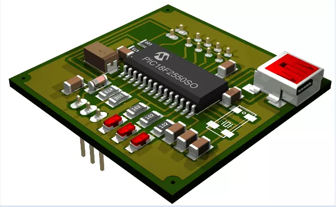
Technology has advanced and electronics are not left behind, as can be seen in the previous image, the first printed circuit boards were totally disorganized, large, heavy and not very efficient, but even so, they fulfilled their function, this gave way to the first electrical and electronic devices, such as the first radios, televisions, among others. All components of these plates were through hole.

Man required a little more to be able to develop and innovate much more, so with the passage of time and after a lot of research, trials and errors, he managed to develop quite impressive technology, surface mount circuits, also multi-layer PCBs, This was the beginning of all the development that we have today, since they allowed to miniaturize all the components of a printed circuit board with through hole components, to a simple board much smaller, efficient and which allows the design in both faces of the plate, reducing the size considerably, today these circuits can be found from a simple calculator, to the computers of space shuttles, through our cell phones, computers, microwaves, refrigerators, stoves, headphones, televisions, In any device that works with electricity we can find printed circuits, have you thought that it would be n Our existence as humans if we didn't have a simple printed circuit board? Impressive!!

Remember that, if you are a maker, engineer or passionate about the world of electronics, you can have your PCB designs manufactured at JLCPCB, for a small sum of money you can have your plates with a professional finish and in a reduced time to to be able to carry out your projects to the next level !!

Syed Zain Nasir

I am Syed Zain Nasir, the founder of <a href=https://www.TheEngineeringProjects.com/>The Engineering Projects</a> (TEP). I am a programmer since 2009 before that I just search things, make small projects and now I am sharing my knowledge through this platform.I also work as a freelancer and did many projects related to programming and electrical circuitry. <a href=https://plus.google.com/+SyedZainNasir/>My Google Profile+</a>

Share
Published by
Syed Zain Nasir