What are DLD Logic Gates? Symbol | Truth Table | Simulation

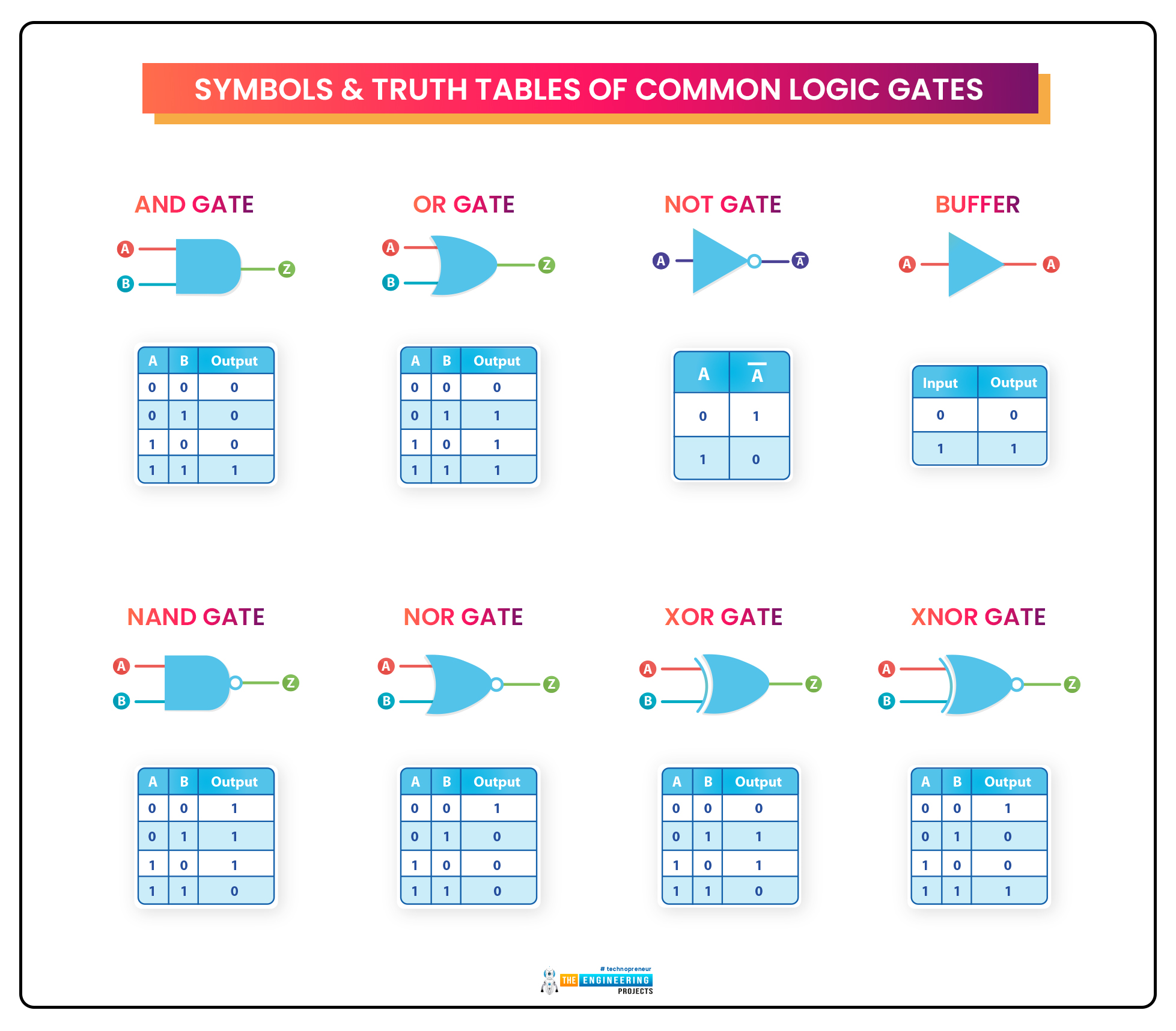
Hello Mentees! I hope you all are doing well. In today's article, we'll learn about the very basic pillar of Digital Logic Circuits i.e. Logic Gates. As we know, the digital world depends on Boolean digits either 0 or 1. So, there's always a need to perform different operations on these boolean numbers i.e. addition, subtraction, multiplication, shifting etc. In order to perform these operations on the binary signals, we use Digital Logic Gates in DLD circuits.

So, let's have a look at What is a Logic Gate:

What is a Logic Gate?

  • Logic Gates are designed to perform a specified operation(i.e. addition, bit shift etc.) on the input signals and generate the output signal.
  • For example, a simple NOT gate takes a single binary input and returns its inverse in the output, i.e.
    • If Input is 0, the Output will be 1.
    • If Input is 1, the Output will be 0.
  • We can design Logic gates using basic electronic components i.e. resistor, diode, transistor, etc. However, in order to design gates for commercial use, two main manufacturing technologies are used, i.e:
  • TTL(Transistor-Transistor Logic): TTL Logic gates use NPN & PNP Bipolar Junction Transistors in their circuitry i.e. 7400 series.
  • CMOS(Complementary Metal Oxide Silicon): CMOS Logic Gates use MOSFET or JFET transistors(i.e. 4000 series)yea ri and are quite popular because of their ultra-quick response.

Symbolic Representation

  • Each Logic gate is assigned a symbol for its representation, which simplifies the designing of their circuit diagrams.
  • The symbolic representation of 4 basic logic gates is as follows:

Truth Table

  • Every logic gate has a truth table(also called a logical table), used to provide the output states for all the possible combinations/conditions of its inputs.
  • It's a convention to write the outputs in the right-side columns and the inputs in the left-side columns.
  • The truth table of NOT Gate(used to inverse input), is shown in the below figure:
Input
Output
0 1
1
0
  • As you can see in the above figure, the table has 2 rows in total giving us all the possible input conditions.
  • The number of rows in a truth table depends on the number of inputs used. The formula is, if we have "n" number of inputs in a logic gate, its truth table will have 2n rows in total. So, if we have 2 inputs, the rows of its truth table will be 22 = 4.

Truth tables are useful in Boolean and mathematical operations as the relationship between the Input and Output can be understood at a glance.

Now let's have a look at the Circuit Designing of Logic Gates:

Logic Gates Circuit Designing

As we discussed earlier, different Manufacturing Techniques are used to design logic gates. These techniques decide the characteristics of the logic gates i.e. response time, noise immunity, voltage level for logic shifting etc. We can use simple electronic components i.e. diode, transistor, resistor etc. to design logic gates. The normal practices for designing logic gates with simple electronic components are:

  • RTL (Resistor-Transistor Logic)
  • DTL ( Diode-Transistor Logic)
  • ECL (Emitter-Coupled Logic)
  • DRL (Diode-Resistor Logic)

Such logic gates are quite simple in designing and normally have quite low response time and may also provide false output because of noise. So, in order to overcome these issues, these two manufacturing techniques are used:

  • TTL(Transistor-Transistor logic)
  • CMOS(Complimentary Metal oxide Semiconductors)

Simple NPN and PNP transistors are used in TTL logic gates and thus have better response time as compared to basic logic gates. In the CMOS technique, MOSFET and FET are used to control the logic and thus provide the best response time and are quite immune to noise. So, among all these manufacturing techniques, CMOS is considered the most popular technique for logic gate designing.

Logic Gates Designing with Basic Components

Here is an example of an AND Gate design with a Diode-Resistor Logic(DRL) and a NAND gate designed with Diode-Transistor Logic (DTL):

As you can see in the above figure, these circuits are quite easy to design, as simply using diodes, resistors, and transistors. But these circuits are not used in commercial ICs because of their high power loss(pull-up resistor) and gate delay(propagation delay). That's why, CMOS and TTL are considered the better option to design digital logic gates.

TTL Logic Gates

In TTL Logic Gates, NPN and PNP transistors are used for designing logic gates. The ideal TTL logic gate is the one that gives the LOW(0) Logic at 0V and HIGH(1) Logic at 5V. In a real TTL Logic Gate, the logic will be considered LOW(0), if the voltage level lies between 0-0.8V and the logic will be considered HIGH(1), if the voltage level is in the range of 2-5V. The voltage level between 0.8-2V is considered a "no man's land" and normally external pull-up or pull-down resistors are used to avoid this region. Examples of TTL Logic Gates ICs are 74Lxx, 74LSxx, 74ALSxx, 74HCxx, 74HCTxx, 74ACTxx etc. The switching voltage varies from group to group according to their internal structure and material used. 

CMOS Logic Gates

In CMOS Logic Gates, FET(Field Effect Transistor) and MOSFET are used to design the logic gates. CMOS logic gates provide a LOW(0) logic, if its voltage is in the range of 0-1.5V and it will give HIGH(1) logic, if it's in the range of 3-18V. The below table shows the voltage levels of both TTL and CMOS logic Gates:

Logic Gates
LOW(0)
HIGH(1)
TTL
0-0.8V
2-5V
CMOS
0-1.5V
3-18V

Now, let's have a look at the Types of Logic Gates:

Types of Logic Gates

  • There are numerous types of Logic gates available based on the quantity of input/output channels and the type of logic to be applied.
  • Based on the specified logic, gates are divided into 3 basic types, i.e.
    1. AND Gate.
    2. OR Gate.
    3. NOT Gate.
  • These 3 basic gates are the building blocks of all advanced logic gates. So, we can design any advance logic gate with these 3 basic logic gates.
  • The most commonly used Advance Logic Gates are:
    1. NAND Gate.
    2. NOR Gate.
    3. XOR Gate.
    4. XNOR Gate.
  • The above-mentioned 7 logic gates are the most commonly used ones. Following logic gates are not that common but are in practice:
    • MIN(Minimum) Logic Gate.
    • MAX(Maximum) Logic Gate.
    • INH(Inhibit) Logic Gate.
    • MAJ(Majority) Logic Gate.
    • IMP(IMPLY) Logic Gate.

It's quite difficult to cover all these gates in a single lecture. So, we will only discuss the basic 7 gates i.e. AND, OR, NOT, NAND, NOR, XOR and XNOR. Today, we will have a brief overview of these 7 logic gates but in the upcoming lectures, we will cover each one of these individually in full detail. Here are the symbols of few logic gates:

So, let's get started:

AND Logic Gate

  • AND Gate is a basic logic gate and gives  HIGH output, when all of its Inputs are HIGH and generates LOW output, if any of its Inputs got LOW.
  • The AND Gate performs the Logical conjunction. We denote it with the DOT between the inputs i.e. A.B = Y where A & B are the inputs and Z is the output.
  • The Inputs in AND Gate is always more than one i.e. Inputs >= 2 and it will always generate a single output.
  • The logical symbol of the AND gate is shown in the below figure:

Truth Table:

  • Here's the truth table of AND gate in tabular form:
A B A.B
0 0 0
0 1 0
1 0 0
1 1 1

As you can see in the truth table of AND Gate, the Output is 1 only when both of its inputs are 1, otherwise, it's 0.

Proteus Simulation of AND Gate

Proteus has an AND Gate component in its components library. We are going to use it to verify the truth table of AND Gate. We will use the following components for designing this AND Gate Simulation:

  1. AND Gate
  2. LED
  3. Logic Toggle
  4. Ground Terminal

Here's the Proteus simulation of all possible states of the AND Gate with 2-inputs:

  • I have placed a Logic State at the inputs of the AND gate and an LED at the output.
  • The LED glows only when both of its Inputs are 1(HIGH).

OR Gate

  • OR gate performs the Disjunction Logic on the inputs i.e. The output will be 1(HIGH), if any of its Inputs is 1(HIGH) and the output will be 0(LOW), if all of its Inputs are 0(LOW).
  • OR Gate is denoted by a plus sign "+" between the inputs i.e. A+B = Y, where A & B are the inputs and Y is the output.
  • Identical to AND Gate, OR Gate also has a minimum of two inputs and only one output.
  • The OR Gate Symbol is shown in the below figure:

Truth Table:

  • Here's the truth table for the OR Gate:
A B A+B
0 0 0
0 1 1
1 0 1
1 1 1

In the case of OR Gate, the output is LOW, only when all of its inputs are LOW, otherwise its HIGH.

Proteus Simulation of OR Gate

  • The simulation is quite the same as that of the AND gate, we simply replace the AND Gate with OR Gate, present in the Proteus components library.
  • The below figure shows that the output LED is OFF, only when both inputs of OR gate are LOW.

NOT Gate

  • In Logic Circuits, the NOT Gate performs the inversion.
  • This is a unary logic Gate that implies it has only one input and a single output.
  • The output of NOT Gate is denoted by a Bar or Complement on the input symbol i.e. If the input is A, the output will be A'.
  • Here's the symbolic representation of NOT Gate:

Truth Table:

  • Here's the truth table of NOT gate, quite simple isn't it?
A B
0 1
1 0
 

Proteus Simulation of NOT Gate

  • Grab the NOT Gate from the Proteus components library.
  • Attach LED and logic toggle at output and input respectively.
  • Here are the results:

So, today we discussed the basic logic gates i.e. AND, OR and NOT Gate and simulated them in Proteus. In upcoming lectures, we'll use these gates to design advance gates and circuits. Take care!!!

JFET Applications | Constant Current Source | Chopper

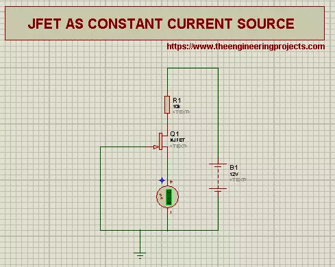
Hi Pupils, Welcome to another Experiment of Proteus at The Engineering Projects. Previously, we saw what are the Junction Field Effect Transistors. Today we'll learn about some of the applications of Junction Field Effect Transistors.

Just before the Experiment, it is useful to revise that: Transistors are three terminal, unipolar Devices. The terminals of Junction Field Effect Transistor are named as :
  • Drain
  • Source
  • Gate
The Gate Terminal is common to both Source and Drain. Prior to start, let's clear some Concepts about Junction Field Effect Transistor.

Resistor

Resistor is an electrical device. we define the resistors as:
"A Resister is a two terminal Passive electrical device that shows the electrical resistance and is useful in almost every Circuit.
Resistors can be used to reduce or control the flow of current , terminate transition lines and such other functions.

Pinch off voltage

The basic Definition of Pinch off voltage is:

"The voltage applied between the Drain and the source at which the current maximum current flows through the circuit provided the Gate voltage is zero is called the Pinch off voltage."

when the value of voltages is less than the pinch off region, the voltage enters to another region called ohmic region of JFET and the transistor acts as a resistor in this region.

Controlling Voltage

The Controlling Voltage of Junction field effect transistor is defined as: "The controlling Voltage is the voltage of transistors from gate to source.  To set its value, the Voltage from gate to source is made negative and it is referred as Vgs." FET's are widely used in the worlds of electronics because of their size and the performance. We'll apply JFET's in the making of two of circuits:
  1. Constant Current Source.
  2. Chopper.
During the Implementation of the Circuits, we'll use N-type JFET because of the better flow of electron of this kind of JFET. In N-type JFET the majority charge carriers are electrons. I am going to explain it one after the other.

Constant Current Source

A Field Effect Transistor can be use as a constant current Source. That spell out that if JFET's are designed so, they can provide a constant current across the load resistor, no matter how much current is provided at its input. The ability is due to the near horizontal line in the drain characteristics of the JFET. Recall that resistor is a two terminal Device that reduces the current flow, divide voltage or adjust signal lines. But, carefully Controlled JFET can be used to overcome the resistance through the resistor that come in between the JFET and the Voltage source. In the circuit, when the Vgs is greater than the pinch off voltage. mathematically,

V-IR>|V|

Implementation in Proteus ISIS

To make the circuit for Constant current Source, we need the Components as:

Component Required:

  1. Junction Field Effect Transistor
  2. Resistor
  3. Ground Terminal
  4. Direct Current Power Supply
  5. Connecting Wires

Procedure

  • Fire up your Proteus Software.
  • Choose the JFET and Resistor from the Pick library through the "P" button.
  • Take the Ground Terminal from Terminals library from the left most tab.
  • Take DC power source from the "Generator mode".
  • To measure the Current we'll add a DC ammeter from the "Virtual Instrument Mode".
This is the step where the Circuit should be arranged so, to get the required output.
  • Connect the Source with the Drain thorough a wire.
  • Join the Ground Terminal with the wire that connects Source and Gate.
  • Connect the Components on the Working area according to the diagram:
  • Double Click the Battery and give it a value of 9 volts.
  • Double click the voltmeter and change the display Range to milliamps.
  • By the same token, Double tap the resistor and give it the value of 1k ohm.
NOTE: you can also use a variable resistor.
  •  Record the values of the ammeter.
  • At first observations, Change the value of resistor to 1kohm.
  • Pop the play button.
The ammeter shows the value of the 0.40 miliamps.
  • Take seven reading by changing the value of resistor and make a table.
    Resistance Current
    1k ohm 0.40 *10-3
    2k ohm 0.40 *10-3
    3k ohm 0.40 *10-3
    4k ohm 0.40 *10-3
    5k ohm 0.40 *10-3
    6k ohm 0.40 *10-3
    7k ohm 0.40 *10-3
     
The same experiment can be done by varying the value of battery and recording the values.

Chopper

A Chopper is the application of Transistor that show us the output as the square wave. We define the Chopper as: "Chopper is an electronic circuit used to take the amplified Direct current by using some type of transistor or other device." One can use any kind of transistor  e.g Bipolar Junction Transistor tor make the Chopper circuit. But, Junction Field Effect Transistors are better for this purpose due to the field control of the JFETs. In Choppers, the FET act as a variable resistance.   Lets rush towards Proteus to apply the circuit.

Implementation of Choppers in Proteus ISIS

  • Fire up your Proteus ISIS.

Material Required

  1. Junction Field Effect Transistor
  2. Resistor
  3. Alternating current source
  4. Ground
  5. Oscilloscope
  • Pick the Vsine , Resistor and JFET from the Pick library by the mean of "P" button.
  • Take the Oscilloscope form "Virtual Instrument Mode" and fix it just above the Circuit.
  • Connect Channel A just after the AC source and channel B with the Source.
  • Put the Ground terminal below the circuit by choosing it from "Terminal".
  • Change the value of resistance connected to AC as 100ohm.
  • Change the value of resistance connected to Source as 200ohm.
  • Give the frequency to 1000Hz and Amplitude of 12V to Vsine.
  • Join the circuit according to the image given below:
Seems like our circuit is complete now.
  • Press the Play button to simulate the graph.
  • Set the Value of Channel A to 1V.
  • Set the channel B to 20V.
The Output of the circuit is:   This Conversion is important in some Circuits. The output of the Chopper is in the form of square waves. Thus, today we learnt about the JFET along with the applications of JFET as Constant current and Chopper in detail and saw their Implementation in the Proteus.

Prevent Data Loss Risk In Raid-Based Storage

Hi Guys! Hope you’re well today. Happy to see you around. In this post today, I’ll detail how to prevent data loss risk in raid-based storage. RAID (Redundant Array of Independent Disks) is a data storage virtualization technology used for data redundancy and performance improvement in an Operating System. It has redefined how storage systems store and retrieve data, and its architecture comprises multiple physical disk drive components distributed over one or more logical units.

Prevent Data Loss Risk In Raid-Based Storage

RAID levels vary from RAID 0 to RAID 51 (and beyond). Different levels have different types of redundancy offered; however, a compromise has to be made when it comes to fault tolerance and performance. Although different RAID levels provide significant protection mechanisms against data loss due to hardware failure of hard disks, the technology is not invincible. Therefore, it is advisable to safeguard your data from any unexpected loss when using a RAID array. If one of the hard drives in a RAID storage array fails, one should consider replacing it instantly. Not doing so or delaying it for too long can cause unexpected data loss as it is highly likely that the other hard drives will fail soon. This is because the entire batch of hard drives in a RAID array often has the same manufacturing date and service life. The type, manufacturer, and other atmospheric variations play an important role in the service life of the hard drives.

Contact Data Recovery Specialist

Preventing to get into such conditions of severe data loss is something you should never divert your focus from because it can be debilitating. Especially, it is more complicated to recover data when it comes to a complex storage system. If you are not well-versed in the required knowledge, you should not take the risk of opting for the DIY mode for recovering the lost data from your RAID system. At such times, it is recommended to contact a reliable data recovery specialist. Doing so can help rebuild the RAID system, bypass the hard drive failures, and examine if any updates are needed in the residing virtualized architecture. This can make the recovery attempt quite time-consuming but reassuringly successful. But for this, it is necessary to make sure that you are choosing the right service provider with proper experience and expertise to recover data in varied data loss events.  

Maintain a Back-up

Different types of RAID configurations operate on different redundancies to diminish data loss and develop a storage system architecture that can provide data loss prevention. Monitoring and recording a RAID array usage is an essential task to be included in the data recovery strategy for efficient business continuity. In severe conditions, the pre-defined recovery strategies may not be helpful and can cause severe data loss. Hence, it is crucial to maintain a back-up and be prepared for such unfortunate cases of system failure or data loss. In such severe conditions of RAID failure, the entire data can disappear forever. Even if a corrupted hard drive overtakes the RAID array's redundancy and the hard disks fail abruptly, it is possible to rebuild your RAID array and recover your data by getting in touch with an expert data recovery professional. Among a few renowned data recovery service providers, Platinum Data Recovery Services has been a prominent name in offering considerate services like G-RAID data recovery and other types of RAID data recovery services when your data has been disappeared or made inaccessible due to corrupted hard drives, flash drives, memory cards, or RAID. That's all for today. I hope you've enjoyed reading this article. If you have any questions, you can approach me in the section below. I'd love to help you the best way I can. Thank you for reading the article.

Introduction to Arduino MKR NB 1500

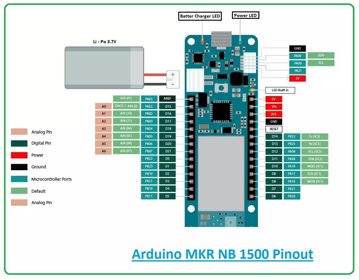
Hi Guys! Hope you’re well today. Happy to see you around. In this post today, I’ll walk you through the Introduction to Arduino MKR NB 1500. The Arduino MKR NB 1500 is mainly developed for working in remote areas where no power or internet connection is available. This board is based on a SAMD21 Cortex-M0+ 32bit low power microcontroller and comes with an operating voltage of 3.3V. Admit it. The Arduino board is a remarkable addition to the development of many automation and embedded projects. These boards are incorporated with a series of digital and analog pins that can be connected with the expansion boards or other breadboards. Most of the Arduino boards are integrated with 8-bit Atmel AVR microcontrollers. And all these boards incorporate different flash memory size to store the code. The two-way serial communication is added in the boards and some boards are given with the facility of the USB port that is used for the direct connection with the computer systems and to program and test the boards on the go. Arduino is an open-source platform that means you can edit and modify the hardware and software based on your requirements. The Arduino IDE software is used to program all kinds of Arduino boards. These boards are programmed using C and C++ language. I suggest you read this post all the way through, as I’ll walk you through the Introduction to Arduino MKR NB1500 covering datasheet, pinout, features, programming, pin description, and applications. Let’s jump right in.

Introduction to Arduino MKR NB 1500

  • The Arduino MKR NB 1500 is an Arduino board based on the SAMD21 Cortex-M0+ 32bit microcontroller that is mainly developed for applications in remote areas with no power or internet connection. On-field monitoring systems use these Arduino boards.
  • These are 22 digital I/O pins incorporated on the board. 7 analog and 12 PWM pins are also included in the chip.
  • The Rx and Tx pins are added to the board for the UART serial communication where Rx is used to receive the serial data and Tx is used to transmit the serial data.
  • Moreover, I2C and SPI communication protocols are also included in the device.
  • The power delivered to the board by USB is 5V. Plus, the board also incorporates a Li-Po charging circuit that makes the board run in two ways: either from the external 5V source or from battery power.
  • The clock speed of the oscillator is 32.768 kHz (RTC), 48 MHz which is required for the synchronization of the internal functions.
  • You can also interface the micro-sim with the board, however, micro-sim is not provided with the board. You need to purchase it separately.
  • You can interface breadboard with this board, giving you the ability to actually test and run your project on a breadboard before switching to the PCB design of the electrical circuit.
  • The board’s flash memory is 256KB. And it doesn’t incorporate EEPROM memory while the SRAM memory is 32KB.
  • The Arduino Program (sketch) is stored in the flash memory and SRAM memory is used to generate and manipulate variables when it runs.

Arduino MKR NB 1500 Datasheet

Before you apply this device to your electrical project it’s better to scan through the datasheet of the device that features the main characteristics of the board. You can download the datasheet of Arduino MKR NB 1500 by clicking the link below.

Arduino MKR NB 1500 Pinout

The following figure shows the pinout diagram of Arduino MKR NB 1500. There are three LEDs on the board. One is a built-in LED, and the other power LED and battery charger LED.

Arduino MKR NB 1500 Pin Configuration

Hope you’ve got a brief idea about this board. In this section, we’ll discuss the pin description of the pins incorporated on the board.

Digital I/O Pins

There are total 8 digital I/O pins integrated on the board which you can use as an input or output according to the requirements. They remain either HIGH or LOW. When they are HIGH they receive 5V and when they are LOW they receive 0V.

Analog Pins

There are total 7 analog pins incorporated on the board. As they are analog pins, they can get any number of values in opposed to Digital pins that only get two values i.e. HIGH or LOW

PWM Pins

The board comes with 12 PWM pins on board. When these pins are activated, the board generates analog result with digital means.

SPI Pins

This board incorporates SPI (serial peripheral interface) pins that are mainly employed to develop the communication between the controller and other peripheral devices such as sensors or shift registers. Two pins… MISO (Master Input Slave Output) and MOSI (Master Output Slave Input) are used for SPI communication. These pins are used to receive or send data by the controller.

I2C Pins

I2C is a two-wire communication protocol. That uses two lines i.e. SDA and SCL. The SDA is a serial data line mainly used to carry the data while SCL is a serial clock line mainly used for the synchronization of all data transfer through the I2C bus.

UART Pins

This device supports UART serial communication. Two pins Rx and Tx are used for the transmission and receiving of serial data.

Battery Connector

If you want to power up the board with the battery be sure to find the female 2 pin JST PHR2 Type connector. Polarity:  while you look at the board connector pins… Polarity is Left = Positive and Right = GND Vcc – This pin generates 3.3V using the on-board voltage regulator. 5V – This pin generates 5V when powered from the Vin pin of the board or from the USB connector. Vin – This pin provides power to the board using a regulated 5V source. If you supply power using this pin, the power through the USB port will be disconnected. This way you can power the board not using USB.

Arduino MKR NB 1500 Features

Microcontroller = SAMD21 Cortex®-M0+ 32bit low power ARM MCU Power Supply (USB/Vin) = 5V Operating voltage = 3.3V Digital I/O Pins = 22 Analog Pins = 7 PWM Pins = 12 I2C = 1 SPI = 1 UART = 1 DC current per I/O pin = 7mA EEPROM = no SRAM = 32KB Flash Memory = 256KB Supported Battery = Li-Po Single Cell, 3.7V, 1500mAh Minimum External Interrupts = 10 (0, 1, 4, 5, 6, 7, 8, 9, 16 / A1, 17 / A2) Size = 25 x 67 mm Weight = 32gr

Arduino MKR NB 1500 Programming

  • You can program this board using Arduino IDE (integrated development environment) software. This software is launched by Arduino.cc you can get this software by going to their site.
  • This board comes with a built-in Bootloader where you can burn the internal program, setting free from the hassle of burning and testing the program with the external burner.
  • This tiny device incorporates a USB port through which you can connect this device with the computer and run and test the program directly from the computer.

Arduino MKR NB 1500 Applications

This tiny little beast is used for a range of applications. Following are some major applications of this device.
  • Automatic Pill Dispenser
  • USB Joystick
  • USB Trackpad
  • Creating a wireless keyboard
  • Water Level Meter
  • Electric Bike
That’s all for today. I hope you’ve enjoyed reading this article. If you’re unsure or have any questions, you can pop your comment in the section below. I’d love to help you the best way I can. Feel free to share your valuable suggestions around the content we share so we keep producing quality content tailored to your exact needs and requirements. Thank you for reading the article.

AD623 Instrumentation Amplifier Datasheet, Pinout, Features & Applications

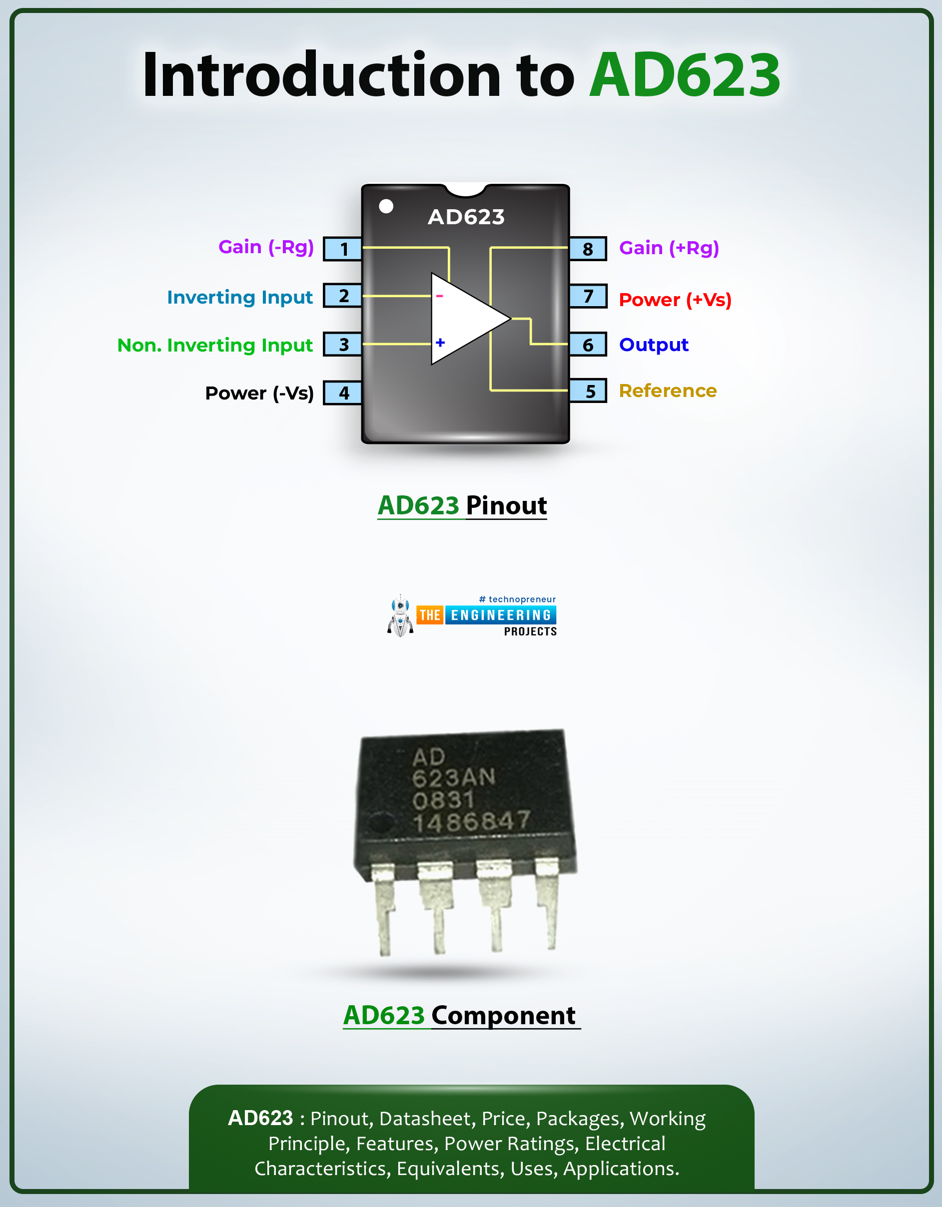
Hi Friends! I welcome you on board. Happy to see you around. In this post today, I’ll walk you through the Introduction to AD623.

The AD623 is an instrumentation amplifier integrated with a rail-to-rail feature. It is mainly used in battery-operated applications due to the low current of 500uA. It features a bandwidth of around 800 kHz which doesn’t require impedance matching since it incorporates buffer amplifiers that are attached to their input pins.

I suggest you buckle up as I’ll detail the complete Introduction to AD623 featuring datasheet, pinout, features, equivalents, and applications. Let’s jump right in.

Introduction to AD623

  • The AD623 is an instrumentation amplifier that falls under the category of differential amplifiers that incorporate buffer amplifiers attached to their input pins, making it a suitable pick for test and measurement equipment.
  • This device doesn’t require impedance matching which is a practice of making one impedance appear like another.

  • Rail-to-Rail feature is used in this amplifier which allows the output voltage to reach its full potential of positive rail voltage or negative rail voltage.
  • In a normal amplifier, this feature is not available as the output voltage of the amplifier is not equal to the supply voltage due to the presence of stage transistors which keep the amplifier from reaching its maximum positive or maximum negative voltage. Rail-to-Rail feature is used to overcome this problem.
  • Moreover, this device comes with very high input impedance, high common-mode rejection ratio, low noise, low drift, and low offset.
  • This kind of amplifier is mainly employed in the circuits where remarkable stability and accuracy is required.
  • Instrumentation amplifier is a type of differential amplifiers where the internal amplifiers are arranged in a way ­– one amplifier is used to generate desired output with enough impedance and the other amplifier is used to buffer each input (+,-)
  • Instrumentation amplifiers can be developed using standard individual amplifiers and precision resistors but also come in an integrated chip. This AD623 amplifier comes in an integrated chip that incorporates laser-trimmed resistors that provide a remarkable common-mode rejection ratio.

AD623 Datasheet

Before you incorporate this device into your electrical project, it’s wise to go through the datasheet of the component that features the main characteristics of the device. Click the link below to download the datasheet of AD623.

AD623 Pinout

The following figure shows the pinout diagram of AD623. The following table shows the pin description of each pin incorporated on the device.
Pin Description of AD623
Pin No. Pin Description Pin Name
1 Inverting Gain Terminal connected to a resistor to set gain value Gain (-Rg)
2 The Inverting input pin of the Op-Amp Inverting Input (IN-)
3 The Non - Inverting Input Pin of Amplifier Non- Inverting Input (IN-)
4 Negative supply terminal Power (-Vs)
5 Output reference input. Normally connected to common Reference
6 Amplifier output pin Output
7 Positive supply terminal Power (+Vs)
8 Non - Inverting Gain Terminal connected to resistor to set gain value Gain (+Rg)

AD623 Features

The following are the main features of AD623.
  • Gain Range = 1 to 1000
  • Set gain with only one resistor
  • Rail to Rail Instrumentation Amplifier
  • Bandwidth = 800KHz
  • Can operate on Single and Dual supply voltage
  • Operating current Max. = 550uA
  • Available Packages = 8-Pin PDIP, VSSOP and SOIC packages

AD623 Equivalents

The following are the alternatives to AD623.
  • JRC4558
  • LM4871
  • IC6283
  • AD620
Before you apply these alternatives to your project, it’s wise to double-check the pinout of the alternatives as it’s quite possible the pinout of the alternatives may differ from the pinout of the AD623.

AD623 Applications

The following are the main applications of AD623.
  • Employed in calibration and test equipment
  • Used in difference amplifiers
  • Used in the control system process
  • Employed in data Acquisition devices
  • Incorporated in low Power Medical instrumentation
  • Used in power-sensitive applications

That’s all for today. That was all about the Introduction to AD623. If you’re unsure or have any questions, you can pop your comments in the section below. I’d love to help you the best way I can. You’re most welcome to share your valuable feedback and suggestions around the content we share so we keep producing quality content customized to your exact needs and requirements. Thank you for reading the article.

Syed Zain Nasir

I am Syed Zain Nasir, the founder of <a href=https://www.TheEngineeringProjects.com/>The Engineering Projects</a> (TEP). I am a programmer since 2009 before that I just search things, make small projects and now I am sharing my knowledge through this platform.I also work as a freelancer and did many projects related to programming and electrical circuitry. <a href=https://plus.google.com/+SyedZainNasir/>My Google Profile+</a>

Share
Published by
Syed Zain Nasir