Hi Guys! I welcome you on board. Thank you for clicking this read. In this post today, I’ll detail the Introduction to Arduino Nano Every.
Arduino Nano Every is a tiny powerful board that is based on the ATMega4809 AVR processor. It comes with a clock speed of around 20MHz and flash memory of around 48KB. It carries two 15 pin connectors on each side of the board that are pin-pin compatible with the Arduino Nano Every.
The low price and small size make this board an ideal pick for the range of electrical projects like electronic musical instruments, low-cost robots, and general development of the small parts of the large projects.
Needless to say, Arduino has been a cornerstone of many electronic projects ranging from simple student projects to ...
Hey Everyone! Hope you’re well today. I welcome you on board. In this post today, I’ll walk you through the Introduction to Arduino MKR Vidor 4000.
The Arduino MKR Vidor 4000 is a powerful board with which you can develop your own controller board. The inclusion of FPGA makes this device unique and separate from other Arduino boards available in the market. With this FPGA feature, you can do audio and video processing which is not possible with other Arduino boards.
Using this device, you can design a real-time computer reading sensor information and the best part is this board is compatible with all other Arduino boards. With this board, you can make all pins PWM signals (on the FPGA block side) for handling the speed of motors. Moreover, you c ...
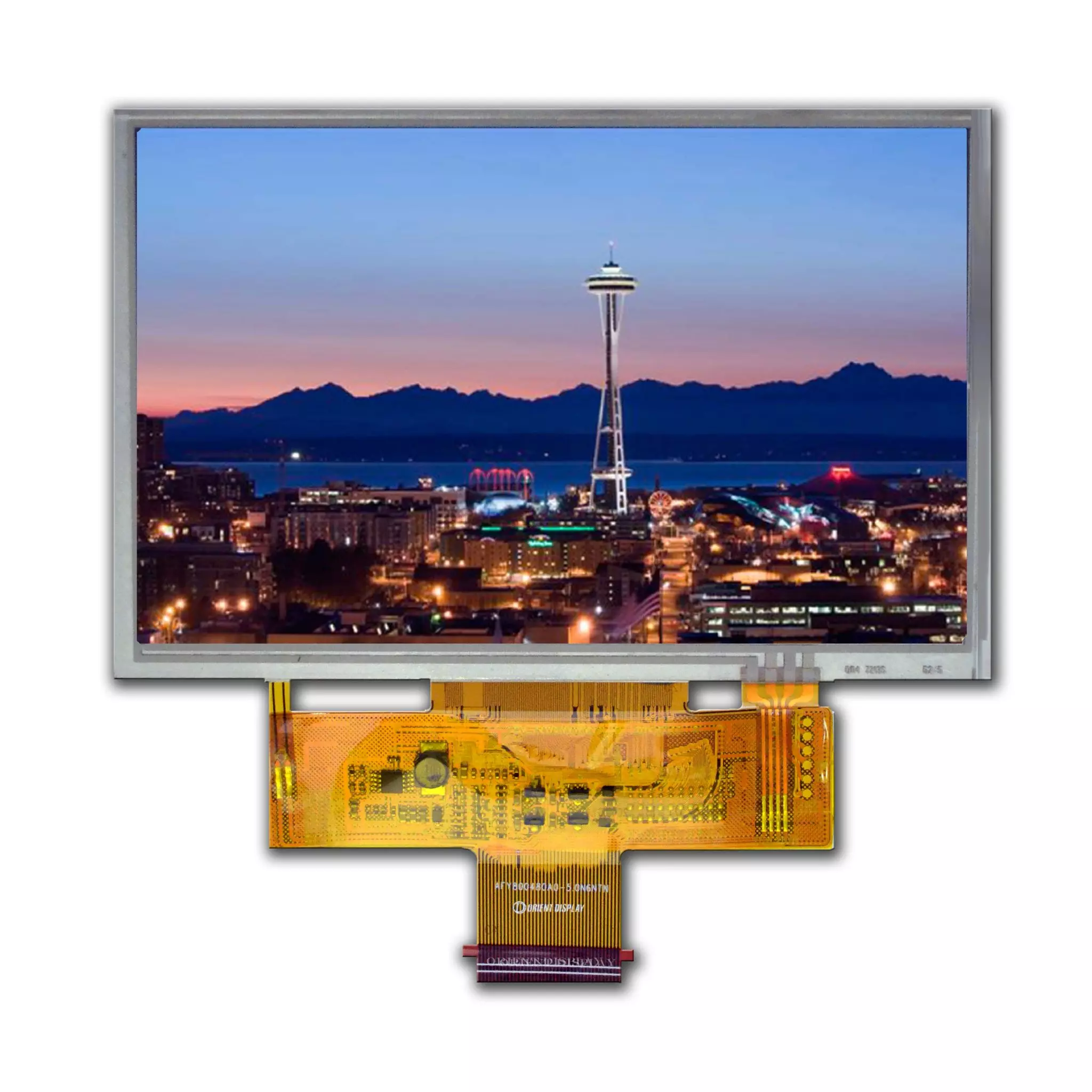
Hello knowledge seekers! welcome to an overview of thin film transistors. I hope you are doing well. Thin film transistors are crucial components of digital display. These transistors have radically transformed our devices and the lifestyle of digital display electronic users. These are the mainstay of major aspects of our lives, from our daily life devices to the big industries, security, medical equipment, and many other departments. These transistors are the driving force behind the success of flat panel displays and most probably, the displays you are reading this article on, such as laptops, mobile screens, monitors, LCDs, etc., using thin film transistors.Today, the motto of this long article is the exploration of thin film transistors. We’ll embark on the foundational introduction o ...