Half Subtractor in Proteus ISIS

Hey Pals! We hope you are doing Great. Today, we are going to design another application of DLD Logical Gates i.e. Half Subtractor. In our previous lectures, we covered Adders in detail, where we studied both Half Adders & Full Adders. Now its time to discuss its reciprocal i.e. Subtractors.

In this session, we'll seek the answers to the following topics:

  1. What is Half Subtractor?
  2. Working Principle of Half Subtractor.
  3. Truth-table of Half Subtractor.
  4. Simulation of Half Subtractor in Proteus using three Logic Gates.
  5. Designing of Half Subtractor with NOR gate.

So, let's get started:

What is Subtractor?

The functionality of Subtractors is exactly the opposite of Adders(we discussed in previous lectures) and defined as:

  • A Subtractor is a simple DLD Electronic circuit, designed using logic gates and is used to subtract binary numbers from one another.
  • A DLD Subtrator generates two outputs(1-bit each) called Difference Bit and Borrow Bit.
  • There are two types of Subtractors available:
  • Half Subtractor. (We are discussing today)
  • Full Subtractor. (We will discuss in the next lecture)

Now, let's have a look at the Half Subtractor:

Half Subtractor

DLD Half subtractors(same as Half Adders) are designed using logic gates and are quite simple in construction. We can define Half Subtractor as:

  • "Half Subtractors are simple digital logical circuits, used to subtract two binary numbers from each other and generate two outputs called Difference Bit and Borrow Bit.
  • The Half Subtractor takes two Inputs A and B and performs the subtraction operation i.e. A - B, where A is called Minuend Bit and B is called Subtrahend Bit.

Working Principle of Half Subtractor

The Half Subtractor has a boolean circuit. It means it works only with the two digits i.e, 0 and 1. The 0 describes the LOW bit and vise versa. It take two bits through the input Terminals and calculate the whole system then shows us the result at the Output Terminals.

Difference in Half Subtractor

The difference is obtained when we perform the minus operation with the second bit from the first bit. the calculator give us the output that is the remaining value of the 1st bit when we deduct the value of 2nd bit from it.

Borrow in Half Subtractor

In the case, when the second bit is higher then the 1st bit, the subtractor borrows a bit from the circuit. this is an essential operation because without this, subtraction can not be proceed further.

Half Subtractor Truth Table

In binary digit difference, the subtraction of 0 with 0 produces the difference 0 and the borrow 0. when the Value is change to A=0 and B=1 then the circuit borrows a bit and both the bits becomes 1 hence we get Difference=1 and borrow=1. When the inputs are A=1 and B=0 then we simply get the value Difference=1 and Borrow=0. At the same token, when A=1, B=1 then the result we get is Difference=0, Borrow=0. Using all these concepts we get the Truth Table as:
A B Difference Borrow
0 0 0 0
0 1 1 1
1 0 1 0
1 1 0 0
In this tutorial we'll learn to design Half subtractor in two ways:
  1. Half Subtractor using three Logic Gates.
  2. Half Subtractor using only NAND Gate.

DID YOU KNOW???????????

Half subtractors are used to limit the force of audio or Radio signals.

Half Subtractor Using three Logic Gates

In this type of formation we use three Logic Gate given below:
  1. XOR Gate
  2. NOT Gate
  3. NAND Gate
When we look at the working of the Half Subtrator, we'll find that the working of the Difference mode of the Half Subtractor is same as the XOR Gate because we that that XOR Gate is the one that gives the output HIGH only when the inputs have different values from each other and vise versa. Just have a look at its Truth Table:
A B A XOR B
0 0 0
0 1 1
1 0 1
1 1 0
Therefore, we simple use the XOR Gat for the function of Difference. When we look at the Function of Difference. we use one AND Gate. A NOT Gate is attached with the one of the input of AND Gate. One may wonder, why we are using the two Gate when we can use the NAND Gate. but the point is, we just need the inverse condition of just one input. Therefore we use this arrangement.

Proteus simulation for Half Subtractor sing Three Gates

Material Required

  1. XOR Gate
  2. AND Gate
  3. NOT Gate
  4. LED-RED
  5. Ground Terminal
  6. Connecting Wires

DID YOU KNOW?????????????

Arithmatic Logic Unit uses the Half Subtractor for the functioning.
  • Begin you Proteus Software.
  • Choose first four Components from Pick Library through "P" Button.
  •  Arrange the Logic Gates one after the other one the working area just as shown in the image:
  • Arrange two Logic Toggles Just in front of the XOR Gate.
  • Get one LED and Set it Just after the XOR Gate.
  • Repeat the step with the with AND Gate.
  • Go to Terminal Mode>Ground attach a ground Terminal with each LED.

DID YOU KNOW?????????????????

One can also use the Logic Probe to Get the output instead of LED.
  • Connect all the Components through wires in accordance with the image below:
  • Change the values at the Input one after the other and notice the output.

Half Subtrator using NOR Gate

Sometimes, you need to make the Circuit as simple as you can. Or you can only use one gate then it is also possible to make the whole circuit using just one gate i.e, NOR Gate. when we look at the definition, it says A NOR Gate is the one that shows the output HIGH only when the Input are LOW. So, one can use the NOR Gate in different ways just by using the connection in a specific way. Let's see how can we do this.

Proteus Simulation of Half Subtractor using NOR Gate

Material Required
  1. NOR Gate
  2. Logic Toggle
  3. LED-RED
  4. Ground Terminal
  5. Connecting Wire
  • Choose the Required Material.
  • Arrange the NOR Gates with respect to the image given next:
 
  • Set Logic Toggles in front of Gate 1.
  • Attach the LED's with the output of Gate two and 5.
  • Ground each LED.
  • Join all the devices through Connecting wires with the help of this image:
You will Observe that this circuit works as the half subtrators when you will change the Value of Logic Toggles. Thus today we Learned what are Half Subtrator, How does the Truth table of Half Subtractor is designed, How can we design the Circuit of Half Subtractor with three Gates as well as using just a NOR Gate. If you want to learn more, you can visit the site for other tutorials as well.

Moving into your New Build: Tips and Tricks

Hello Learners! We welcome you on the Board. We hope you are doing Great. Today we'll talk about the Tips that will be useful and functional Tips that will work best for you if you are thinking to shift in the new build. If statistics are to be believed, the UK is something of a new-build heaven. Every year an estimated 247,000 more houses are built than demolished. On the face of things, new-build properties seem the dream. Remember the days of worrying about a lack of damp-proof course in older properties. Or, what about that chimney stack that can't be moved, but acts as a total eyesore in your front room. While more traditional problems might have been erased, new ones have come in their place. Today's guide is all about showcasing how you can extract the most from your new-build, and not join the army of movers that are riddled with problems with these properties each year.

Make snagging your top priority

Our first piece of advice is to hold fire with moving your belongings in (if you’re really struggling, look at a self storage company). The reason? Snagging. This is a term that you’ll know plenty about by the time your move is complete. Put simply, it involves identifying all of the minor problems that affect a new-build property. The list can be well and truly endless; it might be a door that doesn’t shut properly, or a socket that doesn’t work. It’s not uncommon to uncover hundreds of these small problems. With furniture in place, it’s difficult to carry out. Start on an empty room and see how you go. If you’re allowed (some developers won’t permit it), source a snagging company before completing.

Bonus tip: some problems ARE expected

Want some 'good' news? Some problems are expected. For example, let's talk about condensation. As your house is still drying out, you will see signs of it and in the short-term at least, it's not a major problem. You may also spot a salty substance on bricks. Again, this forms part of the drying out process, and needn't be taken seriously in the early days.

Be cautious with the heating

On the subject of drying out, we would urge you to exercise caution when it comes to turning the heating on. Your move might be in the middle of winter, but if you ramp up the thermostat too much you’ll find that cracking soon starts to occur because of shrinkage. Again, this is one of those unfortunate issues that occur with new builds.

You won't have everything included

Finally, this is where you need to double-check every piece of documentation that your developers have sent over. Contrary to popular belief, your new property probably isn’t going to resemble the beautiful showroom you were given the grand tour of. Instead, there will be all sorts that is missing. This could range from blinds and curtains, right the way to house numbers, door bells and everything in-between. There will be some items that are included, but are probably not up to your specification either. In other words, prepare for magnolia walls and cream carpets. If you can establish what is included in advance, you can even negotiate for higher-spec items before the basics are installed.

IRF1010E MOSFET Datasheet, Pinout, Features & Applications

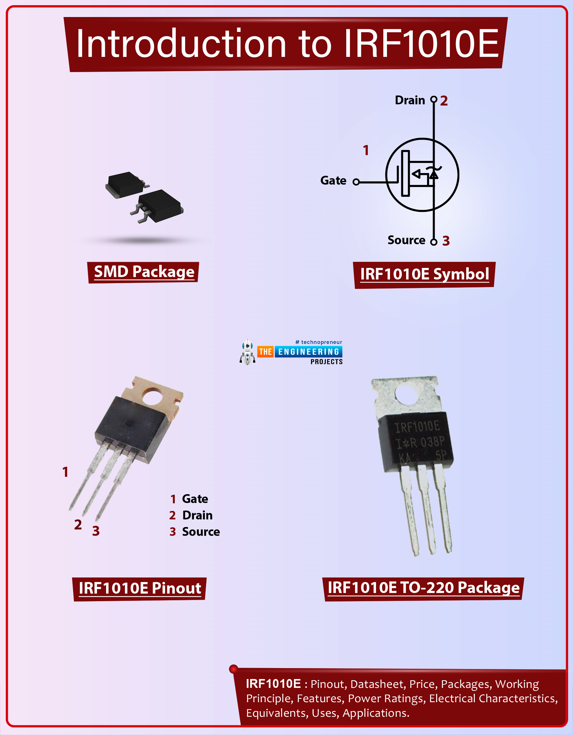
Hi Guys! I welcome you on board. Happy to see you around. In this post today, I’ll walk you through the Introduction to IRF1010E.

The IRF1010E is an N-channel power MOSFET that comes with low turn-on resistance and is mainly used in fast-switching applications. The maximum power dissipation of this device is 170W and the pulsed drain current is quite high i.e. 330A.

I suggest you buckle up as I’ll detail the complete Introduction to IRF1010E covering datasheet, pinout, features, and applications. Let’s get started.

Introduction to IRF1010E

  • The IRF1010E is an N-channel power MOSFET mainly employed for fast-switching applications.
  • This chip is a three-terminal device with terminals drain, source, and gate. It is a voltage-controlled device as opposed to a bipolar junction transistor that is a current-controlled device and comes with terminals: base, collector, and emitter.

  • The gate terminal in IRF1010E is used for the biasing of the device while the source terminal is the area from where electrons enter the channel while the drain terminal is the area from where electrons leave the channel.
  • The gate terminal stands between the source and drain terminals. And the channel width is handled by the voltage on the gate terminal.
  • The main principle of this device is based on controlling the voltage and current between drain and source terminals. The MOS capacitor is the key component that plays a crucial role in the functionality of the device.
  • The MOSFET works in two ways i.e. in depletion mode and enhancement mode. During depletion mode, when no voltage is applied across the gate terminal, there is maximum conductance across the channel. However, when the voltage is applied across the gate terminal, it results in decreasing the channel conductivity.
  • While, on the other hand, the enhancement mode works exactly opposite to the depletion region. Here when there is no voltage, there is no conductance across the channel. While when voltage is applied, it results in increasing the conductance.
  • There are two types of MOSFET available in the market i.e. P-channel MOSFET and N-channel MOSFET. This device IRF1010E falls under the category of N-channel MOSFET where electrons flow as the charge carriers in contrast to P-channel MOSFETs where holes are the major charge carriers.
  • This IRF1010E MOSFET comes with low turn-ON resistance, making it a right fit for low-drop switching applications. The low drop results in low power loss, hence ensuring greater efficiency. This device is also used for high-efficiency applications.

IRF1010E Datasheet

It is wise to go through the datasheet before incorporating this device into your project. This datasheet features the main characteristics of the component. Click the link below to download the datasheet of IRF1010E.

IRF1010E Pinout

The following figure represents the pinout diagram of IRF1010E.   The following table details the pin description of each pin embedded on the chip.

IRF1010E Features

The following are the main features of IRF1010E.
  • Developed with advanced process technology
  • Used in Fast switching
  • Fully avalanche rated
  • Operating Temperature Max. = 175ºC
  • The voltage across GATE and SOURCE Max. = 20 V
  • Continuous current allowed through DRAIN Max. = 81A
  • The voltage across DRAIN and SOURCE Max. = 60V
  • It’s a Fifth generation HEXFET
  • Pulsed DRAIN current Max. = 330A
  • Power dissipation Max. = 170Watt

IRF1010E Alternatives

The following are the alternatives to IRF1010E.
  • IRFB4110
  • IRFB4310Z
  • IRFB4115
  • IRFB4410
  • IRF1407
  • IRFB4110G
  • IRFB4310ZG

Double-check the pinout of the alternatives before incorporating them into your project as the pinout of the alternatives might differ from the pinout of IRF1010E.

IRF1010E Applications

This device is used in the following applications.
  • Employed in speed control units
  • Incorporated in PWM applications
  • Used in Relay drivers
  • Employed in Switch mode power supply
  • Used in Lighting systems
  • Used in any switching applications

That’s all for today. I hope you find this article helpful. If you have any questions, you can approach me in the section below. I’ll try to help you the best way I can. You’re most welcome to share your valuable feedback and suggestions around the content we share so we keep producing quality content customized to your exact needs and requirements. Thank you for reading the article.

CA3130 MOSFET BiMOS Op-Amp Datasheet, Pinout, Features & Applications

Hi Everyone! Hope you’re well today. I welcome you on board. In this post today, I’ll walk you through the Introduction to CA3130.

The CA3130 is a BiMOS Operational Amplifier that comes with MOSFET at the output. The term BiMOS suggests that it projects the advantage of both Bipolar and CMOS op-amp technology.

This IC comes with high bandwidth due to bipolar op-amps and consumes less current due to CMOS op-amp, making it a perfect fit for mobile jammers and voltage follower circuits.

I suggest you read this post all the way through as I’ll detail the complete Introduction to CA3130 covering datasheet, pinout, features, and applications. Let’s get started.

Introduction to CA3130

  • The CA3130 is a BiMOS Operational Amplifier that contains MOSFET at the output. This chip consumes less current and features high bandwidth.
  • This device has high input impedance due to MOSFETs which implies that when an output voltage of the sensor is connected to the inverting or non-inverting terminals of the op-amp, the output voltage from the sensor will not be disturbed since the op-amp will not act as a load to the sensor.

  • If you’re looking for a device with high input impedance, less power consumption, and high bandwidth, this chip might be the answer.
  • CA3130 is an eight-terminal electronic IC that comes with a Common Mode Rejection Ration (CMRR) of 80dB.
  • It is widely used in frequency generators and noise detectors.
  • The input terminal current of this device is 1mA and the supply current is 10mA.
  • The CA3130 features inverting and non-inverting pins like other op-amps. If the voltage at the non-inverting pin is high, the output across the inverting pin will be high, otherwise, it will be low.
  • Pins 1 & 5 are offset null pins used to nullify the offset produced when two input pins are combined. When the input pins of the op-amp are combined with each other, the voltage at the output should be zero. But no operational amplifier is ideally perfect. So when two inputs are combined together, it results in the offset. The offset null pins are used to null that effect.
  • Pin 8 is called Strobe that is mainly used to turn off the output stage. It is also employed for phase compensation in comparators.

CA3130 Datasheet

Before you incorporate this device into your electrical project, it’s wise to go through the datasheet of the device that features the main characteristics of the component. Click the link below and download the datasheet of CA3130.

CA3130 Pinout

The following figure shows the pinout diagram of CA3130. The following table shows the pin description of each pin incorporated on the chip.
Pin Description of CA3130
Pin No. Pin Description Pin Name
1,5 When the input pins of the op-amp are combined with each other, the voltage at the output should be zero. But no operational amplifier is ideally perfect. So when two inputs are combined together, it results in the offset. The offset null pins are used to null that effect. Offset Null Pins
2 The Inverting pin is also given a fixed voltage which is compared with the (IN+) Inverting Input (IN-)
3 The Non-Inverting Pin of the comparator gives a variable  voltage to compare Non-Inverting Input (IN+)
4 This pin is connected to the ground of the system (Negative voltage can also be used) Ground (VCC-)
6 This is the output pin of the op-amp Output
7 This VCC pin offers the operating voltage for the Op-Amp. For CA3130 it is up to +16V VCC+
8 Allows you to turn off the output stage Strobe

CA3130 Features

  • Op-amp laced with MOSFET at the output
  • Input Terminal current = 1mA
  • Wide power supply Range i.e. for single supply – 5V to 16V and for dual supply – ±2.5V to ±8V
  • Sink current Max. = 20mA
  • Source current Max. = 22mA
  • Output Voltage Max. = 13.3V
  • Supply current = 10mA
  • Common Mode Rejection Ration (CMRR) = 80dB

CA3130 Alternatives

The following are the alternatives to CA3130.
  • LM311
  • LM324
  • LM358
  • LM741
  • LM339
Check the pinout of the alternatives before incorporating them into your electrical project as the pinout of the alternatives might differ from the pinout of the CA3130.

CA3130 Applications

The CA3130 is used in the following applications.
  • Incorporated in DAC circuits
  • Used in voltage follower circuits
  • Employed in mobile jammers
  • Employed in Oscillator circuits
  • Used in frequency generator/distorter
  • Used in Peak Signal/Noise detectors

That’s all for today. Hope you find this article helpful. If you have any questions, you can pop your comment in the section below. I’d love to help you the best way I can. Feel free to share your valuable feedback and suggestions around the content we share so we keep coming back with quality content customized to your exact needs and requirements. Thank you for reading the article.

INA219 Current Sensor Module Datasheet, Pinout, Features & Applications

Hi Friends! Hope you’re well today. I welcome you on board. Today, I’ll walk you through the Introduction to INA219.

The INA219 is a current sensor module that incorporates the I2C protocol for submitting the data obtained through sensing current, voltage, and power. It is a bi-directional zero drift current/ power sensing module mainly used in digital multimeters and power profilers.

I suggest you read this post all the way through as I’ll detail the complete Introduction to INA219 covering datasheet, pinout, features, and applications. Let’s get started.

Introduction to INA219

  • INA219 is a current/power sensor module mainly employed to sense the power, voltage or current where up to 128 samples can be averaged together to get filtering in noisy environments. This data is then submitted to a microcontroller using the I2C bus.

  • This device features an I2C protocol mainly used to transmit data between devices. The I2C protocol comes with two wires SDA and SCL. The SDL is a serial data line that carries the data while SCL is a serial clock line that carries the clock signal and ensures the synchronization of data transfer over an I2C bus.
  • In the I2C protocol, one device acts like a master and the other as a slave. Using this communication protocol you can attach multiple slaves with a single master whereas you can also control single or multiple slave devices with multiple masters.
  • INA219 can be easily incorporated with microcontrollers and Arduino boards and with devices that come with an I2C bus interface.
  • It also contains a 2W 0.1 Ohms 1% rated shunt resistor mainly employed to fulfill the current measuring requirements.
  • This sensor module is a key part of the power monitoring systems. The power input of this device ranges from 3V to 5.5V and the target voltage is up to +26V.

INA219 Datasheet

It is better to go through the datasheet of the device before you embed this device into your electrical project. The datasheet features the main characteristics of the module. Click the link below to download the datasheet of INA219.

INA219 Pinout

The following figure shows the pinout diagram of INA219. The following table represents the pin description of each pin incorporated into the module.
Pin Description of INA219
Pin No. Pin Description Pin Name
1 Sensed Input line - VIN-
2 Sensed Input line + VIN+
3 Input voltage VCC
4 Connected to ground GND
5 Serial clock line that carries the clock signal SCL
6 Serial data line that contains the data SDA

INA219 Features

  • Contains 2C- or SMBus-compatible interface
  • Comes with up to +26V target voltage
  • Power Input Range = 3.0V-5.5V
  • Can Sense Bus Voltages ranging from 0 to 26 V
  • Up to 128 samples are averaged to get filtering in noisy environments.
  • Capable of up to ±3.2A current measurement, with ±0.8mA resolution
  • Contains ohm 1% 2W current sense resistor
  • Board Dimension = 0.8 x 0.9 inch (l x w x h)

INA219 Applications

  • Used in power monitoring systems
  • Employed in power profiler
  • Used in digital multimeter

That’s all for today. Hope you find this article helpful. If you’re unsure or have any questions, you can approach me in the section below. I’d love to help you the best way I can. Feel free to share your valuable feedback and suggestions around the content we share so we keep coming back with quality content customized to your exact needs and requirements. Thank you for reading the article.

Syed Zain Nasir

I am Syed Zain Nasir, the founder of <a href=https://www.TheEngineeringProjects.com/>The Engineering Projects</a> (TEP). I am a programmer since 2009 before that I just search things, make small projects and now I am sharing my knowledge through this platform.I also work as a freelancer and did many projects related to programming and electrical circuitry. <a href=https://plus.google.com/+SyedZainNasir/>My Google Profile+</a>

Share
Published by
Syed Zain Nasir