1N4007General-purpose silicon rectifier
Pass one polarity. Block the other.
1N4007 is a general-purpose silicon rectifier with two terminals. It conducts conventional current from anode to cathode when forward biased and blocks reverse voltage within its rated limits. The colored band identifies the cathode end of its axial body. The reviewed Vishay 1N4007-E3 uses a DO-41 package. Its 1000 V repetitive reverse rating is the highest in this 1N4001–1N4007 family; its average-current rating is 1 A under the specified lead-length and temperature conditions. A PCB footprint can choose a formed lead spacing, so the page states its authored 10.16 mm pitch explicitly. A small, isolated 9 V RMS AC example shows half-wave rectification without a reservoir capacitor. The output remains pulsating. Forward drop, load current, heating and reverse recovery matter; this general-purpose part must not be treated as a fast-recovery switching diode.
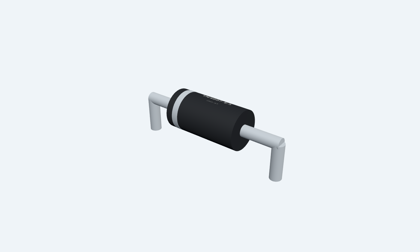

Cathode / bandAnode / forward entry
1N4007-E3DO-41Top view · band at K1 · A2 opposite
Click a lead or use the arrow keys. Top view · band at K1 · A2 opposite
PIN 1 · Cathode / band
CathodeK
Function
The banded end of the rectifier.
How to connect
Connect to the positive half-wave output in the example.
Electrical note
This page uses the KiCad convention 1 = cathode, 2 = anode. The manufacturer identifies polarity by the band, not numeric package pins.
PIN 2 · Anode / forward entry
AnodeA
Function
Conventional forward current enters here and leaves the cathode.
How to connect
Connect to the isolated low-voltage AC source in the example.
Electrical note
Forward voltage depends on current and temperature; 0.7 V is only the teaching assumption used below.
At a glance
General-purpose silicon rectifier
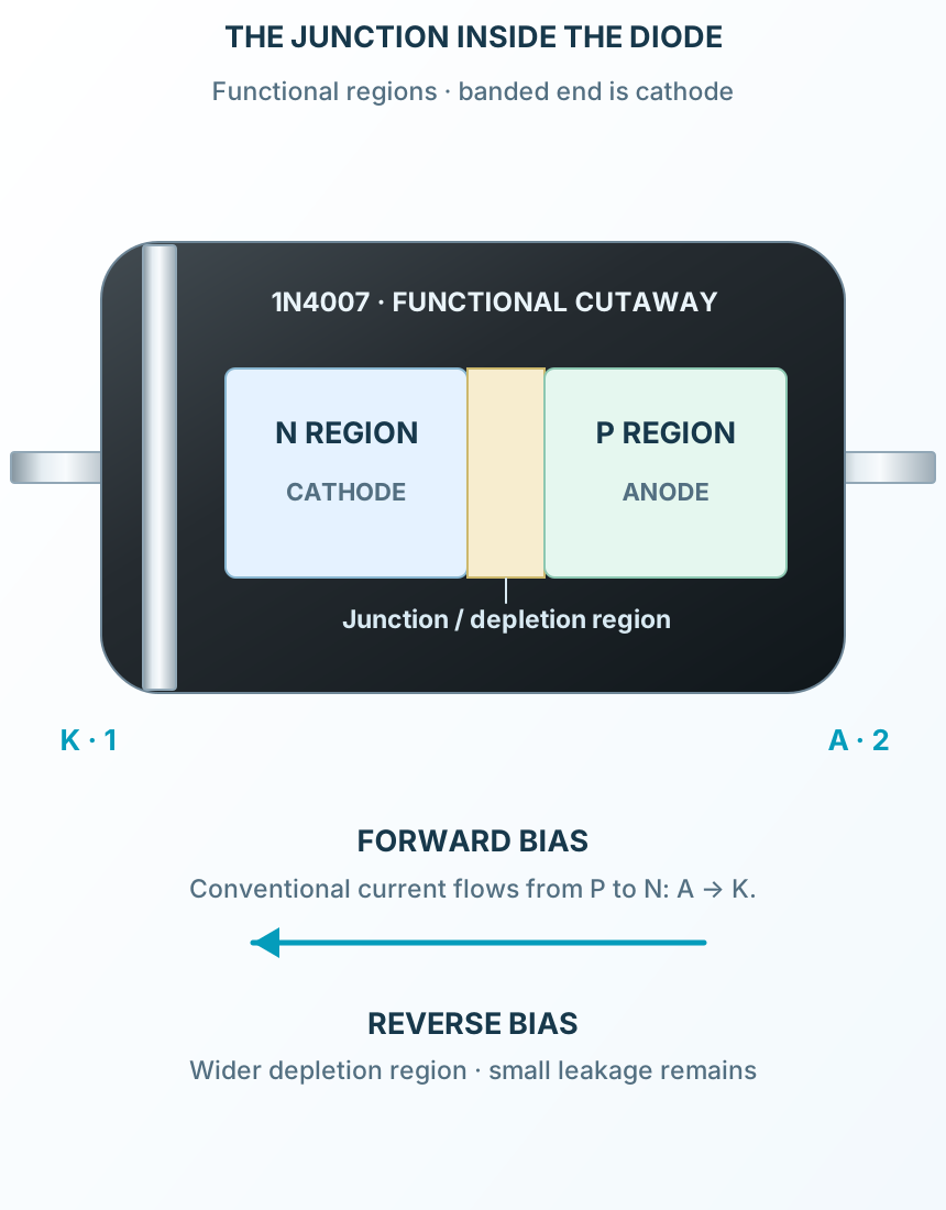
Forward bias allows current through the external load; reverse bias blocks most current. The diode is not a current limiter and the output of one-diode rectification is not smooth DC.
1000 V · VRRMReverse peak rating
1 A · stated mountingAverage forward current
1.1 V · IF = 1 AForward drop maximum
150 °C · maximumJunction limit
Operating profile
1N4007-E3
Selected device and polarity
Key parameters and their test conditions
- Reference
- Vishay document 88503Conditions / notes: Electrical revision 29 April 2020
- Selected family
- 1N4007-E3Conditions / notes: Commercial, RoHS-compliant base part
- Package
- DO-41 / DO-204ALConditions / notes: Molded axial body with plated leads
- Cathode identification
- Colored body bandConditions / notes: Independent of how the part is rotated
- Page / KiCad numbering
- 1 K · 2 AConditions / notes: Editorial PCB convention; manufacturer uses polarity names
- Authored lead spacing
- 10.16 mmConditions / notes: A formed horizontal mounting choice, not a fixed straight-lead package pitch
Package details
Follows the selected physical package
- Manufacturer
- Vishay General Semiconductor
- Part number
- 1N4007-E3
- Package
- DO-41
- Connections
- 2 pins
- Mounting
- Through-hole
- Lead pitch
- 10.16 mm · formed for this footprint
- Package code
- DO-204AL
- Thermal reference
- Rated current depends on lead length, copper and ambient temperature
Connections by function
Select a pin to open its function, electrical notes and wiring guidance.
Cathode / band1 pins
Anode / forward entry1 pins
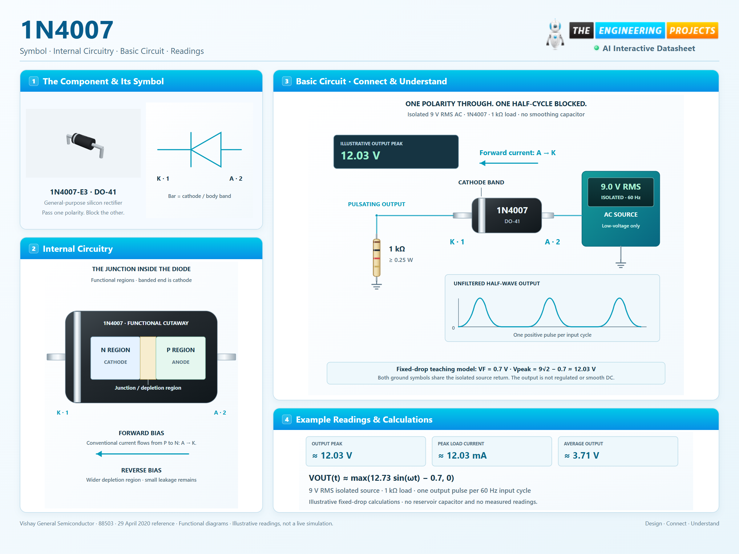
Identify the band
The banded end is cathode K, numbered 1 in this PCB convention.
Pass the positive half-cycle
The anode must be positive enough relative to cathode to forward-bias the junction.
Recognize the ripple
With no filter capacitor, current returns to zero through each blocked half-cycle.
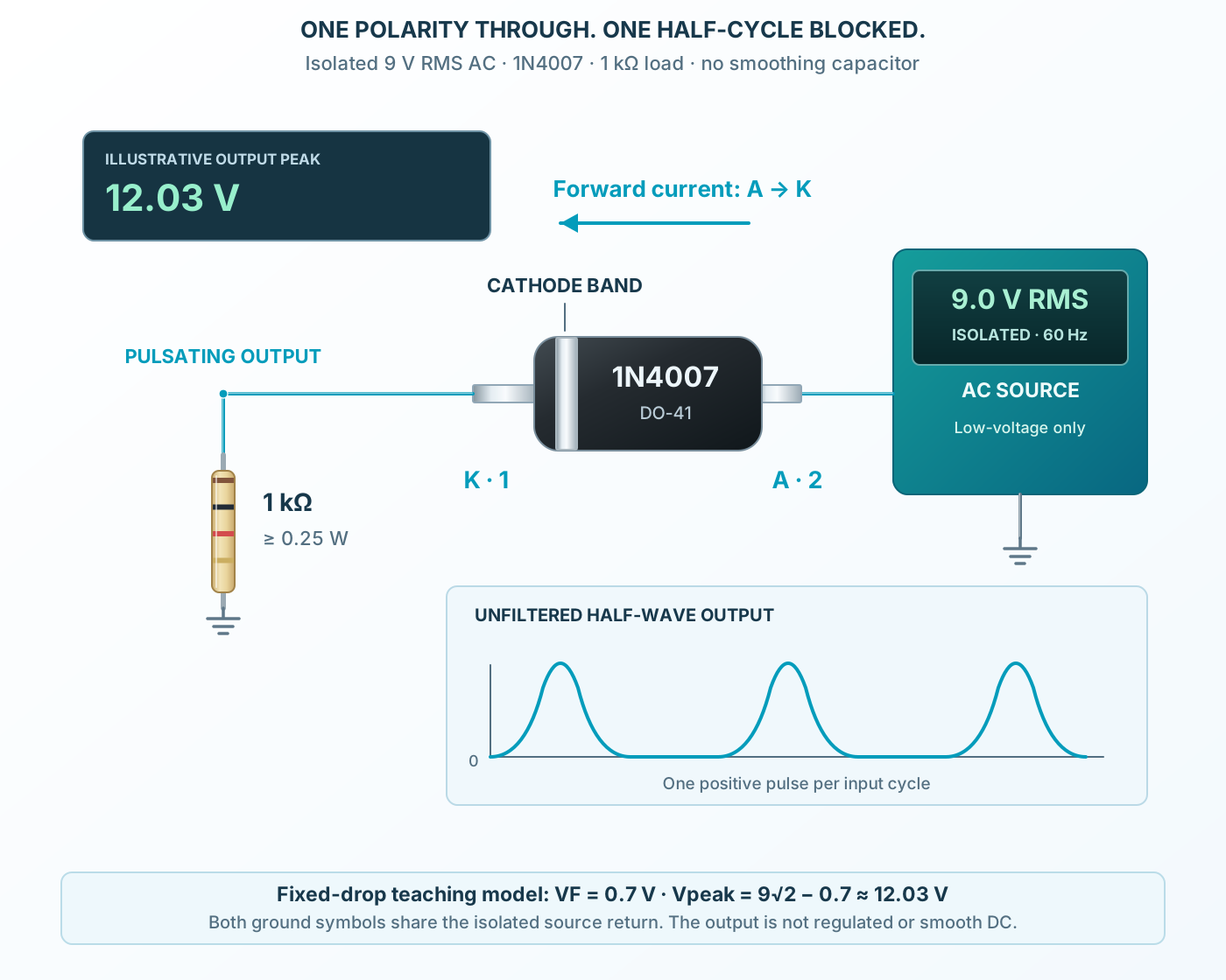
For 9 V RMS sine input, the peak is about 12.73 V. A fixed 0.7 V drop model gives about 12.03 V peak and 12.03 mA peak into 1 kΩ; the negative half-cycle is blocked.
Pin reference
Select a pin to explore its function and connection.
2 pins
| Pin | Signal | Type | Function |
|---|---|---|---|
| K | Cathode | The banded end of the rectifier. | |
| A | Anode | Conventional forward current enters here and leaves the cathode. |
No pins match. Try a signal name or choose All pins.
Selected device and polarity
Manufacturer scope and page conventions
Manufacturer specifications 6 parameters
| Parameter | Value | Conditions / notes |
|---|---|---|
| Reference | Vishay document 88503 | Electrical revision 29 April 2020 |
| Selected family | 1N4007-E3 | Commercial, RoHS-compliant base part |
| Package | DO-41 / DO-204AL | Molded axial body with plated leads |
| Cathode identification | Colored body band | Independent of how the part is rotated |
| Page / KiCad numbering | 1 K · 2 A | Editorial PCB convention; manufacturer uses polarity names |
| Authored lead spacing | 10.16 mm | A formed horizontal mounting choice, not a fixed straight-lead package pitch |
No specifications match. Try a parameter name or a unit.
Do not infer electrical polarity solely from left/right placement after rotation.
Voltage and current ratings
Selected 1N4007 column
Manufacturer specifications 7 parameters
| Parameter | Value | Conditions / notes |
|---|---|---|
| Repetitive reverse peak VRRM | 1000 V | Maximum |
| RMS reverse voltage | 700 V | Maximum |
| DC blocking voltage | 1000 V | Maximum |
| Average rectified current | 1 A | TA 75°C; 9.5 mm lead length |
| Single half-sine surge | 30 A | 8.3 ms, superimposed on rated load |
| Square-wave nonrepetitive surge | 45 / 35 / 30 A | 1 / 2 / 5 ms at TA 25°C |
| Junction / storage range | −50 to +150°C | Absolute limits |
No specifications match. Try a parameter name or a unit.
Surge ratings apply to specified waveforms and are not repetitive load-current targets.
Electrical characteristics
Test conditions remain attached to each figure
Manufacturer specifications 6 parameters
| Parameter | Value | Conditions / notes |
|---|---|---|
| Instantaneous forward voltage | 1.1 V maximum | IF = 1 A |
| DC reverse leakage at 25°C | 5 µA maximum | Rated DC blocking voltage |
| DC reverse leakage at 125°C | 50 µA maximum | Rated DC blocking voltage |
| Junction capacitance | 15 pF typical | Reverse 4 V; frequency 1 MHz |
| Full-load average reverse current | 30 µA maximum | Full cycle; TL 75°C; 9.5 mm lead length |
| Reverse recovery | No trr guarantee in this reference | Use a specified fast-recovery part where required |
No specifications match. Try a parameter name or a unit.
The 0.7 V example model is not the datasheet maximum at 1 A.
Package and thermal conditions
DO-41 outline and mounting
Manufacturer specifications 7 parameters
| Parameter | Value | Conditions / notes |
|---|---|---|
| Body length | 4.1–5.2 mm | Manufacturer outline |
| Body diameter | 2.0–2.7 mm | Manufacturer outline |
| General outline lead diameter | 0.71–0.86 mm | Check the exact ordered suffix and drawing note |
| Straight lead length | At least 25.4 mm each end | Before forming and trimming |
| Junction-to-ambient resistance | 50°C/W typical | 9.5 mm lead length, PCB mounted |
| Junction-to-lead resistance | 25°C/W typical | Same stated mounting reference |
| Assembly review | Lead bend and copper affect heat flow | Authored land pattern must be checked for the actual part |
No specifications match. Try a parameter name or a unit.
A 1 A current rating does not remove the need for a temperature-rise calculation.
Isolated 9 V AC half-wave circuit
No mains connection and no reservoir capacitor
Manufacturer specifications 6 parameters
| Parameter | Value | Conditions / notes |
|---|---|---|
| AC source | 9 V RMS, 60 Hz sine | Isolated laboratory low-voltage source |
| Anode A2 | AC source active terminal | Other source terminal is common return |
| Cathode K1 | Positive output node | Band faces the load |
| Load resistor | 1 kΩ, at least 0.25 W | From output to source return |
| Diode model | Fixed 0.7 V forward drop | Illustrative approximation |
| Output waveform | One positive pulse per AC cycle | Negative half-cycle blocked; no smoothing |
No specifications match. Try a parameter name or a unit.
Changing to a capacitor-input rectifier changes peak charging current and the required analysis.
Example waveform calculations
For the stated fixed-drop model
Manufacturer specifications 7 parameters
| Parameter | Value | Conditions / notes |
|---|---|---|
| Input peak | Approximately 12.73 V | 9 × √2 |
| Output peak | Approximately 12.03 V | Input peak minus 0.7 V |
| Peak load current | Approximately 12.03 mA | Output peak / 1 kΩ |
| Conduction onset angle | Approximately 3.15° | asin(0.7 / 12.73) |
| Average output | Approximately 3.71 V | Integrated clipped sine; not a regulated DC output |
| Output relation | max(12.73 sin(ωt) − 0.7, 0) | Positive direction and fixed-drop approximation |
| Ripple repetition | 60 Hz | One pulse per 60 Hz input cycle |
No specifications match. Try a parameter name or a unit.
All readings are explanatory calculations, not live measurements.
Practical selection checks
Current, voltage and speed must all fit
Manufacturer specifications 6 parameters
| Parameter | Value | Conditions / notes |
|---|---|---|
| Reverse-voltage margin | Compare with the actual waveform | Include transients and capacitor charging topology |
| Average and peak current | Check both | Capacitor charging can create narrow high-current pulses |
| Temperature | Use loss and mounting conditions | Copper and lead length affect cooling |
| High-frequency converters | Use an appropriately specified diode | General-purpose rectification does not imply fast recovery |
| Inductive loads | Choose a suitable flyback path | Verify surge energy, turn-off needs and diode current |
| SMD alternatives | Separate orderable devices | Do not relabel a different package as the same selected part |
No specifications match. Try a parameter name or a unit.
The page keeps the selected axial reference distinct from faster or differently packaged relatives.
Low-frequency rectifiers
Convert alternating polarity to a pulsating unidirectional output.
Manufacturer application guideReverse-polarity paths
Use with a suitable current and voltage budget.
Manufacturer application guideLow-speed freewheeling
Check the load current, stored energy and required release time.
Manufacturer application guideTake it into ProTech
Find 1N4007 in the Components Library to place its schematic symbol and connect its pins.
Reference page · circuit simulation model not yet availableOpen ProTech