1N4148Small-signal silicon switching diode
A tiny glass junction for fast signal switching.
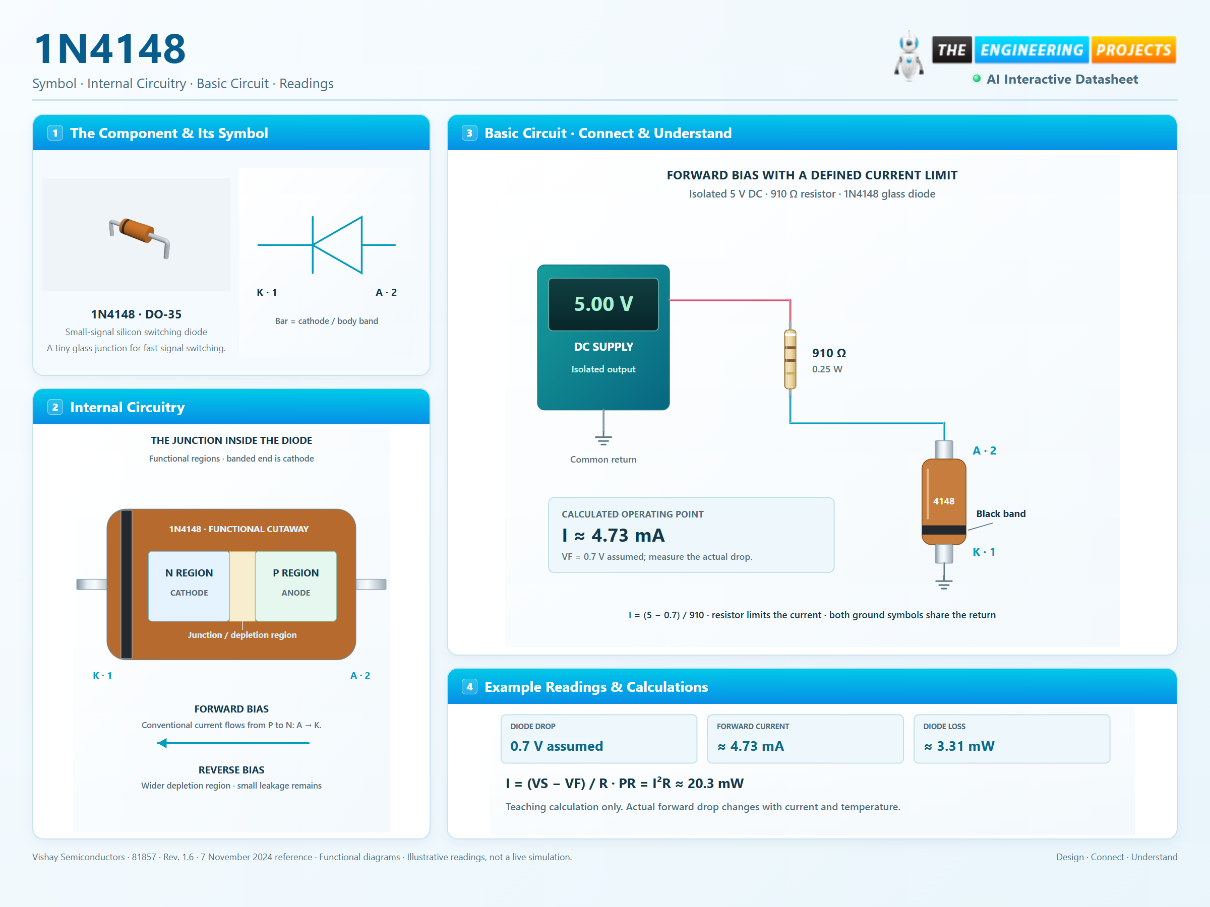
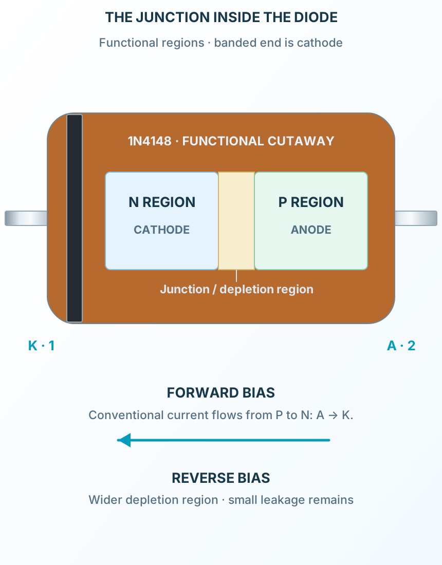
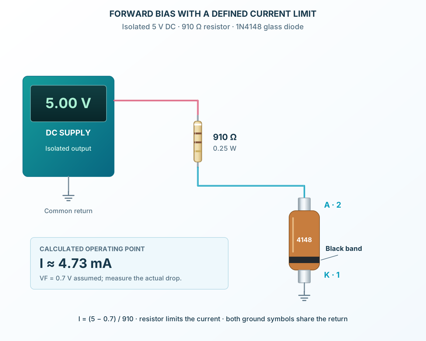
1N4148 is a two-terminal silicon diode for switching small signals. Forward bias allows current from anode to cathode; reverse bias blocks most current while a small leakage remains. A black band on its glass body identifies the cathode. This page follows Vishay’s axial DO-35 device. Its reverse-recovery specification is only a few nanoseconds under defined test conditions, making it useful for signal steering and clipping. It is not interchangeable with a high-current power rectifier simply because both parts have two leads. The basic circuit uses an isolated 5 V DC supply and a 910 Ω resistor to demonstrate forward bias at approximately 4.73 mA. The resistor limits current; the diode does not. Package dimensions, pad numbering and the authored 7.62 mm mounting pitch are documented separately from the electrical ratings.
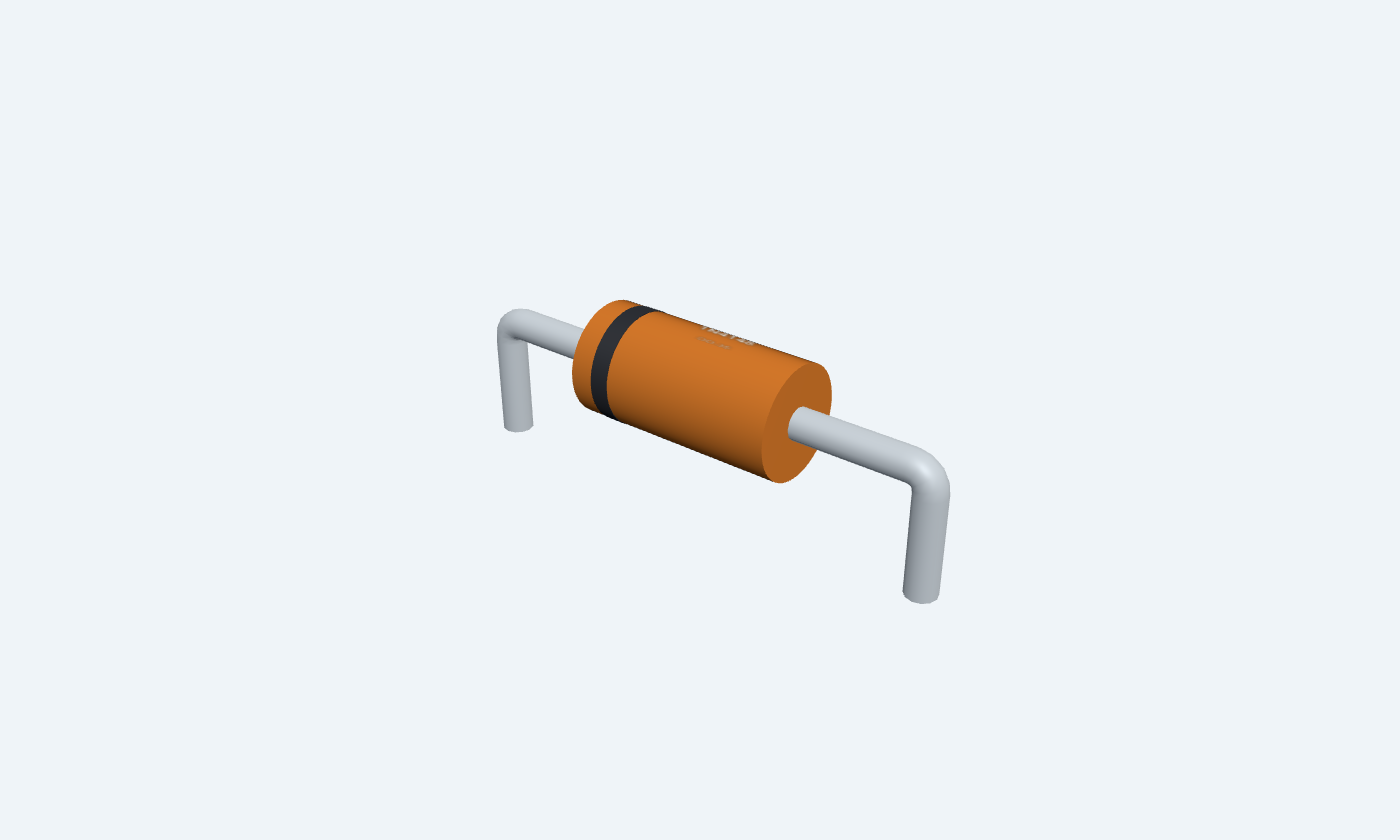

Cathode / bandAnode
1N4148DO-35Band = K1 · other end = A2
Click a lead or use the arrow keys. Band = K1 · other end = A2
PIN 1 · Cathode / band
CathodeK
Function
The black band identifies the cathode.
How to connect
Connect to ground in the forward-bias test circuit.
Electrical note
Pad 1 = K is the page and KiCad convention, not a manufacturer numeric lead designation.
PIN 2 · Anode
AnodeA
Function
Conventional forward current enters the anode and leaves the cathode.
How to connect
Connect to +5 V through the 910 Ω current-limiting resistor.
Electrical note
Forward drop depends on current and temperature; 0.7 V is only an explanatory approximation.
At a glance
Small-signal silicon switching diode
The PN junction conducts in forward bias and blocks in reverse bias within its limits. Keep current, temperature and test conditions attached to every rating.
100 V · absolute maximumRepetitive reverse peak
150 mA · stated test conditionsAverage forward current
4 ns maximum · specified testReverse recovery
175 °C · absolute maximumJunction limit
Operating profile
1N4148
Device and polarity
Key parameters and their test conditions
- Package
- DO-35 / DO-204AHConditions / notes: Glass axial envelope
- Polarity mark
- Black cathode bandConditions / notes: Independent of orientation
- PCB numbering
- 1 = K; 2 = AConditions / notes: Editorial / KiCad convention
- Ordering examples
- 1N4148-TAP / 1N4148TRConditions / notes: Packaging choices in the source
- Formed pitch
- 7.62 mmConditions / notes: Authored horizontal mounting choice
Package details
Follows the selected physical package
- Manufacturer
- Vishay Semiconductors
- Part number
- 1N4148
- Package
- DO-35
- Connections
- 2 pins
- Mounting
- Through-hole
- Lead pitch
- 7.62 mm · formed mounting
- Package code
- DO-204AH
- Thermal reference
- Lead length and lead temperature affect allowable power
Connections by function
Select a pin to open its function, electrical notes and wiring guidance.
Cathode / band1 pins
Anode1 pins
Locate the cathode
Identify the black band; the other end is the anode.
Limit the current
Place 910 Ω in series before applying the isolated 5 V supply.
Observe forward bias
Measure voltage across the diode and current through the resistor. Reverse polarity to observe blocking, within the reverse rating.
With a 5 V source and 910 Ω series resistor, a fixed 0.7 V diode model gives (5 − 0.7) / 910 ≈ 4.73 mA. Actual voltage and current vary with device and temperature.
Pin reference
Select a pin to explore its function and connection.
2 pins
| Pin | Signal | Type | Function |
|---|---|---|---|
| K | Cathode | The black band identifies the cathode. | |
| A | Anode | Conventional forward current enters the anode and leaves the cathode. |
No pins match. Try a signal name or choose All pins.
Device and polarity
Vishay axial 1N4148, not a different SMD suffix
Manufacturer specifications 5 parameters
| Parameter | Value | Conditions / notes |
|---|---|---|
| Package | DO-35 / DO-204AH | Glass axial envelope |
| Polarity mark | Black cathode band | Independent of orientation |
| PCB numbering | 1 = K; 2 = A | Editorial / KiCad convention |
| Ordering examples | 1N4148-TAP / 1N4148TR | Packaging choices in the source |
| Formed pitch | 7.62 mm | Authored horizontal mounting choice |
No specifications match. Try a parameter name or a unit.
Separate package dimensions from the chosen lead-forming pitch.
Absolute maximum ratings
25°C ambient unless specified
Manufacturer specifications 10 parameters
| Parameter | Value | Conditions / notes |
|---|---|---|
| Repetitive reverse peak | 100 V | VRRM |
| Reverse voltage | 75 V | VR |
| Continuous forward current | 300 mA | IF; thermal constraints still apply |
| Average forward current | 150 mA | VR = 0 |
| Repetitive forward peak | 500 mA | IFRM |
| Forward surge | 2 A | 1 µs pulse only |
| Power | 500 mW | 4 mm leads; lead temperature ≤25°C |
| Power | 440 mW | 4 mm leads; lead temperature 45°C |
| Junction maximum | 175°C | Absolute limit |
| Storage | −65 to +150°C | Unpowered storage |
No specifications match. Try a parameter name or a unit.
These are stress limits, not simultaneous normal operating targets.
Electrical characteristics
25°C ambient unless stated
Manufacturer specifications 7 parameters
| Parameter | Value | Conditions / notes |
|---|---|---|
| Forward drop | 1 V maximum | IF = 10 mA |
| Reverse leakage | 25 nA maximum | VR = 20 V |
| Hot reverse leakage | 50 µA maximum | VR = 20 V; junction 150°C |
| High-voltage leakage | 5 µA maximum | VR = 75 V |
| Capacitance | 4 pF maximum | VR = 0 V; f = 1 MHz; AC amplitude 50 mV |
| Recovery, test 1 | 8 ns maximum | IF = IR = 10 mA; measured at reverse 1 mA |
| Recovery, test 2 | 4 ns maximum | IF = 10 mA; VR = 6 V; RL = 100 Ω; measured at 0.1 × IR |
No specifications match. Try a parameter name or a unit.
Recovery time is meaningful only with its test circuit and measurement threshold.
Package and heat flow
DO-35 source outline
Manufacturer specifications 7 parameters
| Parameter | Value | Conditions / notes |
|---|---|---|
| Body length | 3.4 mm maximum | Before lead forming |
| Body diameter | 1.5–1.75 mm | Glass envelope |
| Lead diameter | 0.55 mm maximum | Plated axial leads |
| Untrimmed lead length | 25.4 mm minimum per end | Source outline |
| Thermal resistance | 350 K/W | 4 mm leads; lead temperature held constant |
| Authored PCB lands | 1.6 mm pads / 0.8 mm holes | Engineering starting values |
| Mounting pitch | 7.62 mm | Forming must not stress the glass seal |
No specifications match. Try a parameter name or a unit.
Confirm the ordered part and manufacturing tolerances before fabrication.
Forward-bias bench circuit
Calculated teaching values, not measurements
Manufacturer specifications 8 parameters
| Parameter | Value | Conditions / notes |
|---|---|---|
| Supply | Isolated 5 V DC | Common negative reference |
| Series resistor | 910 Ω, 0.25 W | Between source positive and A2 |
| Diode return | K1 to ground | Black band faces ground |
| Approximate forward drop | 0.7 V | Fixed-drop teaching assumption |
| Estimated current | 4.73 mA | (5 − 0.7) / 910 |
| Resistor dissipation | 20.3 mW | I²R at the teaching operating point |
| Diode dissipation | 3.31 mW | 0.7 × I |
| Reverse-biased test | Swap diode polarity | Only small leakage; remain below reverse limits |
No specifications match. Try a parameter name or a unit.
A measured forward drop will depend on temperature, current and device variation.
Signal steering
Route low-current signals through defined polarity paths.
Manufacturer application guideClipping and clamping
Limit excursions using a suitable series impedance and reference.
Manufacturer application guideFast switching
Use the recovery specification with the actual circuit conditions.
Manufacturer application guideTake it into ProTech
Find 1N4148 in the Components Library to place its schematic symbol and connect its pins.
Reference page · circuit simulation model not yet availableOpen ProTech