AD623Low-power instrumentation amplifier
Measure a small voltage difference with one gain resistor.
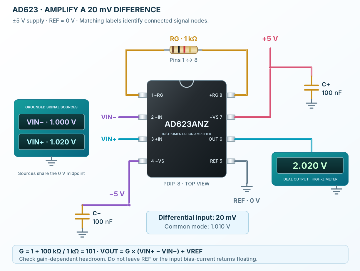
AD623 is an instrumentation amplifier for small differential measurements. Its matched input and subtraction stages reject voltage shared by the two inputs, while a resistor between pins 1 and 8 sets the differential gain. It supports a 2.7–12 V single supply or ±2.5–±6 V split supplies. Its input range can extend slightly below the negative rail under specified conditions, and its output approaches the rails with light loading. Gain-dependent internal headroom must still be checked. This reference selects the AD623ANZ through-hole and AD623ARZ surface-mount grades. A 1 kΩ gain resistor gives G = 101; with ±5 V supplies, grounded REF and inputs of 1.020 V and 1.000 V, the ideal output is 2.020 V.
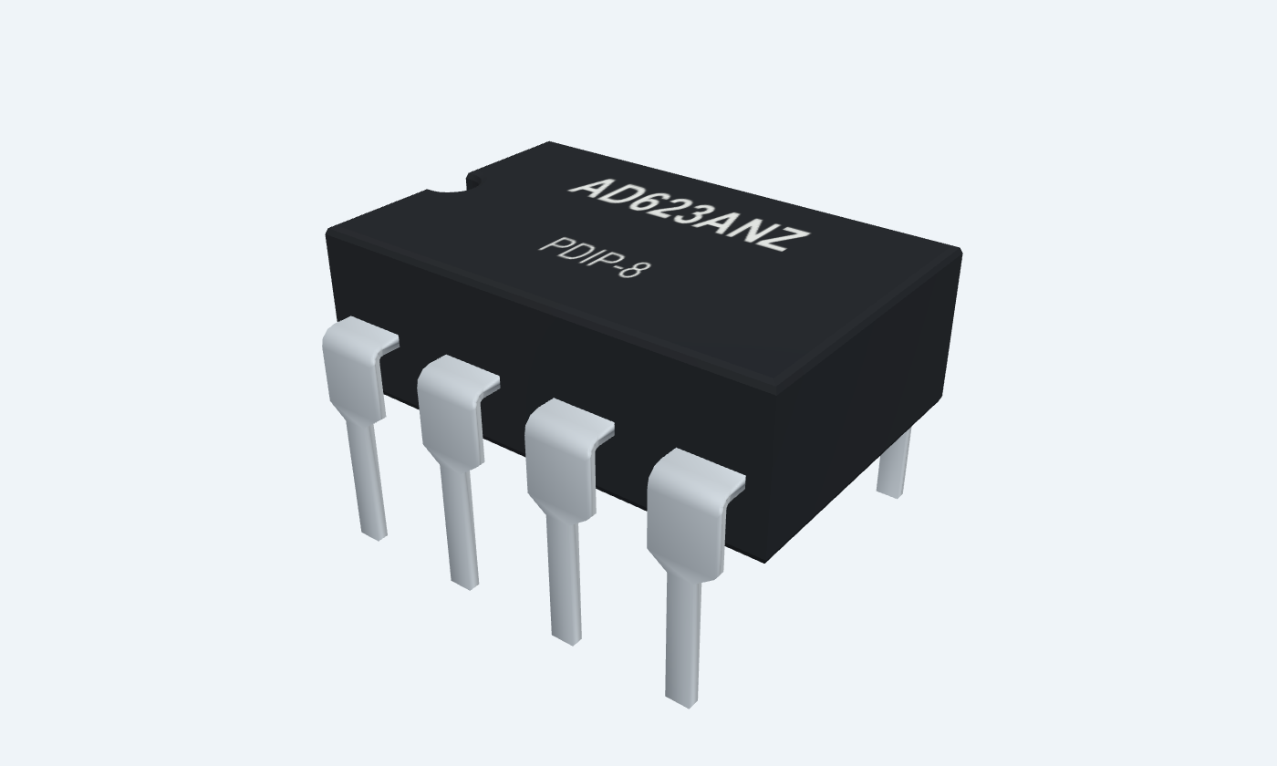
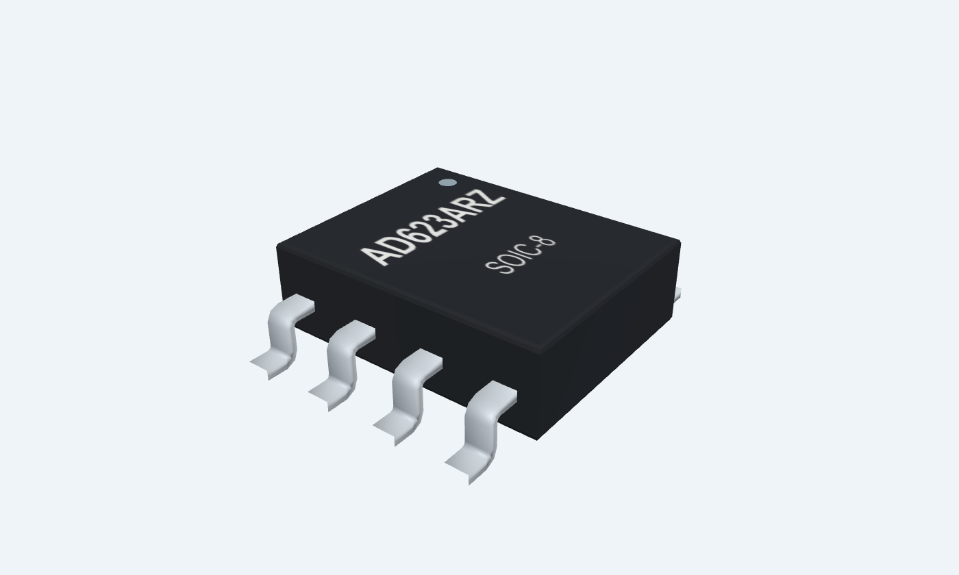

External gain resistorDifferential inputsSupply railsOutput baselineAnalog output
AD623ANZPDIP-8Top view
AD623ARZSOIC-8Top view
Click a lead or use the arrow keys. Top view
PIN 1 · External gain resistor
Gain resistor terminal−RG
Function
Inverting-side connection for the external gain resistor.
How to connect
Connect 1 kΩ to +RG8 for a nominal gain of 101.
Electrical note
Leaving both RG terminals open gives gain 1; never short them together.
PIN 2 · Differential inputs
Inverting signal input−IN
Function
Negative input of the differential measurement.
How to connect
Apply 1.000 V from a source returned to the 0 V supply midpoint.
PIN 3 · Differential inputs
Noninverting signal input+IN
Function
Positive input of the differential measurement.
How to connect
Apply 1.020 V from a source returned to the 0 V supply midpoint.
Electrical note
Both inputs need a DC path for their bias currents.
PIN 4 · Supply rails
Negative supply−VS
Function
Negative rail shared by the internal amplifier stages.
How to connect
Connect −5 V, with 100 nF bypass to the supply midpoint.
Electrical note
In single-supply operation this pin connects to ground; in this split-supply example it is −5 V.
PIN 5 · Output baseline
Output baselineREF
Function
Adds the reference voltage to the amplified differential signal.
How to connect
Connect directly to the 0 V midpoint.
Electrical note
Drive from low impedance; an unbuffered high-resistance divider can degrade rejection and accuracy.
PIN 6 · Analog output
Analog outputOUT
Function
Output follows G × (+IN − −IN) + REF while the internal stages remain in range.
How to connect
Use a high-impedance meter; the ideal example value is 2.020 V.
Electrical note
Near-rail swing depends on load; the device does not reach either rail exactly.
PIN 7 · Supply rails
Positive supply+VS
Function
Positive rail for the device.
How to connect
Connect +5 V with 100 nF bypass to the 0 V midpoint.
PIN 8 · External gain resistor
Gain resistor terminal+RG
Function
Noninverting-side connection for the external gain resistor.
How to connect
Connect the 1 kΩ gain resistor to −RG1.
At a glance
Low-power instrumentation amplifier
The gain resistor controls differential gain, while REF sets the output baseline. Input common mode and output loading determine the usable signal range.
1–1000 V/VProgrammable gain
2.7–12 VSingle supply
305 µA typical at 25°CSingle-supply current
−40 to +85 °CSpecified temperature
Operating profile
AD623ANZ
Operating conditions
Key parameters and their test conditions
- Single supply
- 2.7–12 VConditions / notes: −VS at circuit ground
- Split supplies
- ±2.5 to ±6 VConditions / notes: The example uses ±5 V
- Specified temperature
- −40 to +85°CConditions / notes: Selected A grades
- Gain equation
- G = 1 + 100 kΩ / RGConditions / notes: Nominal range 1–1000
- Single-supply current
- 305 µA typical; 480 µA maximumConditions / notes: 25°C; 625 µA maximum over temperature
- Dual-supply current
- 375 µA typical; 550 µA maximumConditions / notes: 25°C; 625 µA maximum over temperature
Package details
Follows the selected physical package
- Manufacturer
- Analog Devices
- Part number
- AD623ANZ
- Package
- PDIP-8
- Connections
- 8 pins
- Mounting
- Through-hole
- Lead pitch
- 2.54 mm
- Package code
- PDIP-8
- Thermal reference
- See operating and package limits
Connections by function
Select a pin to open its function, electrical notes and wiring guidance.
External gain resistor2 pins
Differential inputs2 pins
Supply rails2 pins
Output baseline1 pins
Analog output1 pins
External gain resistor2 pins
Differential inputs2 pins
Supply rails2 pins
Output baseline1 pins
Analog output1 pins
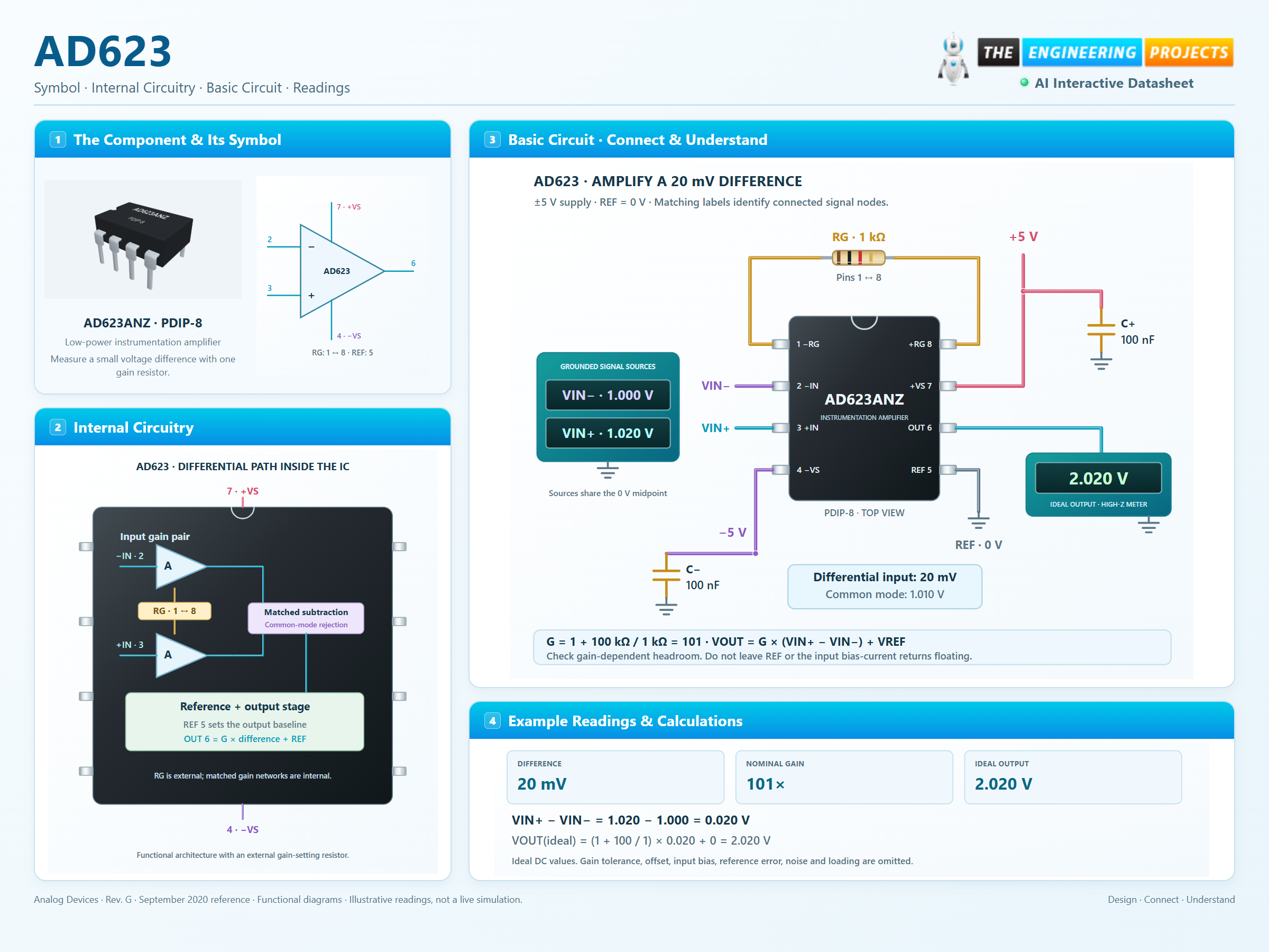
Sense the input pair
The example inputs differ by 20 mV and have a common-mode voltage of 1.010 V. Both sources have a DC return to the supply midpoint.
Set the gain
A 1 kΩ resistor between −RG1 and +RG8 gives 1 + 100 / 1 = 101 V/V.
Reference the output
Grounding REF5 gives an ideal output of 101 × 0.020 = 2.020 V. Offset, resistor tolerance and loading add real errors.
AD623 uses G = 1 + 100 kΩ / RG. Its gain constant differs from AD620 and INA128; matching pin numbers alone do not make those devices interchangeable.
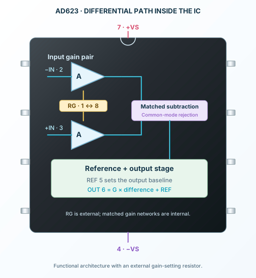
Pin reference
Select a pin to explore its function and connection.
8 pins
| Pin | Signal | Type | Function |
|---|---|---|---|
| −RG | Gain resistor terminal | Inverting-side connection for the external gain resistor. | |
| −IN | Inverting signal input | Negative input of the differential measurement. | |
| +IN | Noninverting signal input | Positive input of the differential measurement. | |
| −VS | Negative supply | Negative rail shared by the internal amplifier stages. | |
| REF | Output baseline | Adds the reference voltage to the amplified differential signal. | |
| OUT | Analog output | Output follows G × (+IN − −IN) + REF while the internal stages remain in range. | |
| +VS | Positive supply | Positive rail for the device. | |
| +RG | Gain resistor terminal | Noninverting-side connection for the external gain resistor. |
No pins match. Try a signal name or choose All pins.
Operating conditions
AD623ANZ / AD623ARZ
Manufacturer specifications 7 parameters
| Parameter | Value | Conditions / notes |
|---|---|---|
| Single supply | 2.7–12 V | −VS at circuit ground |
| Split supplies | ±2.5 to ±6 V | The example uses ±5 V |
| Specified temperature | −40 to +85°C | Selected A grades |
| Gain equation | G = 1 + 100 kΩ / RG | Nominal range 1–1000 |
| Single-supply current | 305 µA typical; 480 µA maximum | 25°C; 625 µA maximum over temperature |
| Dual-supply current | 375 µA typical; 550 µA maximum | 25°C; 625 µA maximum over temperature |
| Absolute supply limit | 12 V total | Allow for supply tolerance and startup transients |
No specifications match. Try a parameter name or a unit.
Input and output headroom still apply throughout the supply range.
Accuracy and bias
A-grade PDIP / SOIC · 25°C
Manufacturer specifications 7 parameters
| Parameter | Value | Conditions / notes |
|---|---|---|
| Gain error, G = 1 | 0.03% typical; 0.10% maximum | Manufacturer output-voltage test interval |
| Gain error, G = 10 / 100 / 1000 | 0.10% typical; 0.35% maximum | Excludes external RG error |
| Input offset VOSI | 25 µV typical; 200 µV maximum | 350 µV maximum over temperature |
| Output offset VOSO | 200 µV typical; 1000 µV maximum | 1500 µV maximum over temperature |
| Total input-referred offset | VOSI + VOSO / G | Do not omit the output-stage contribution |
| Input bias current | 17 nA typical; 25 nA maximum | 27.5 nA maximum over temperature |
| Input offset current | 0.25 nA typical; 2 nA maximum | 25°C |
No specifications match. Try a parameter name or a unit.
MSOP and B-grade limits differ; the values here belong to AD623ANZ and AD623ARZ.
Input and output headroom
Check the operating window at the chosen gain
Manufacturer specifications 7 parameters
| Parameter | Value | Conditions / notes |
|---|---|---|
| Input interval at G = 1 | −VS − 0.15 V to +VS − 1.5 V | Manufacturer test with one input grounded; supply conditions apply |
| Output, 10 kΩ load | −VS + 0.2 V to +VS − 0.5 V | Specified swing at the reference supply |
| Output, 100 kΩ load | −VS + 0.05 V to +VS − 0.15 V | Lighter load allows closer rail approach |
| Input-stage nodes, approximate | VCM + 0.6 V ± G × VDIFF / 2 | Both internal nodes must remain inside their usable range |
| Example internal nodes | About 0.60 V and 2.62 V | VCM = 1.010 V; G × VDIFF / 2 = 1.010 V |
| Example output headroom | 2.020 V on ±5 V rails | Well within the stated 10 kΩ interval |
| REF drive | Low impedance | Avoid floating REF or a high-resistance unbuffered divider |
No specifications match. Try a parameter name or a unit.
The G = 1 input range is not an unconditional input range at every gain and output voltage.
Bandwidth and noise
Typical reference values
Manufacturer specifications 8 parameters
| Parameter | Value | Conditions / notes |
|---|---|---|
| Bandwidth at G = 1 | 800 kHz | Small-signal −3 dB |
| Bandwidth at G = 10 | 100 kHz | Small-signal −3 dB |
| Bandwidth at G = 100 | 10 kHz | Small-signal −3 dB |
| Bandwidth at G = 1000 | 2 kHz | Small-signal −3 dB |
| Slew rate | 0.3 V/µs | Typical |
| Settling to 0.01%, G = 10 | 20 µs | Specified step and supply conditions |
| Input voltage-noise density | 35 nV/√Hz | 1 kHz; add output-stage noise referred through gain |
| Input current-noise density | 100 fA/√Hz | 1 kHz |
No specifications match. Try a parameter name or a unit.
Useful signal bandwidth decreases as gain rises. Large-signal settling and slew limits are separate checks.
20 mV measurement circuit
±5 V supplies · grounded reference
Manufacturer specifications 8 parameters
| Parameter | Value | Conditions / notes |
|---|---|---|
| Input +IN3 | 1.020 V | Grounded source |
| Input −IN2 | 1.000 V | Grounded source |
| Differential / common mode | 20 mV / 1.010 V | Difference / average of the two input voltages |
| RG between 1 and 8 | 1 kΩ | Nominal gain 101 |
| REF5 | 0 V | Direct connection to supply midpoint |
| OUT6 | 2.020 V ideal | Use a high-impedance meter |
| Supply +VS7 / −VS4 | +5 V / −5 V | 100 nF from each rail to midpoint |
| Bulk supply bypass | 10 µF per rail where needed | Manufacturer recommends ceramic plus local bulk bypass |
No specifications match. Try a parameter name or a unit.
The displayed reading is an ideal calculation, not a live measurement. Input bias paths and reference impedance are essential.
Selecting a different gain
RG = 100 kΩ / (G − 1)
Manufacturer specifications 7 parameters
| Parameter | Value | Conditions / notes |
|---|---|---|
| Gain 1 | RG open | Do not fit a short |
| Gain 2 | 100 kΩ | Exact nominal resistor calculation |
| Gain 11 | 10 kΩ | Example of a lower gain setting |
| Gain 101 | 1 kΩ | The illustrated configuration |
| Gain 1000 | About 100.1 Ω | 100 Ω gives nominal 1001; choose tolerance appropriately |
| RG error sensitivity | Resistor tolerance affects gain above unity | Use suitable tolerance and temperature coefficient |
| Output offset example limit | About 21.2 mV | 101 × 200 µV + 1000 µV, excluding other errors |
No specifications match. Try a parameter name or a unit.
Recheck common-mode and output headroom whenever gain changes.
Package and layout
AD623ANZ · PDIP-8
Manufacturer specifications 7 parameters
| Parameter | Value | Conditions / notes |
|---|---|---|
| Through-hole | AD623ANZ · N-8 | 2.54 mm pitch; 7.62 mm nominal rows |
| Surface mount | AD623ARZ · R-8 | 1.27 mm pitch; narrow SOIC |
| Other variants | MSOP and B grades exist | Use their separate package drawings and accuracy columns |
| Gain resistor placement | Close to pins 1 and 8 | Keep series resistance and noise pickup low |
| Input routing | Balanced, quiet paths | Source-impedance imbalance converts bias current to error |
| Reference and ground | Low-impedance, quiet return | Keep digital load current away from measurement returns |
| Footprint provenance | Original TEP starting land patterns | Verify against exact package and fabrication process |
No specifications match. Try a parameter name or a unit.
Package switching preserves physical functions and numbering.
Bridge-sensor interfaces
Amplify small differential bridge signals with gain and common-mode headroom checked together.
Manufacturer application guideThermocouple conditioning
Provide bias-current returns, a suitable output reference and cold-junction compensation elsewhere.
Manufacturer application guideLow-power acquisition
Condition low-level measurements before an ADC while budgeting reference, noise and output-load errors.
Manufacturer application guideTake it into ProTech
Find AD623 in the Components Library to place its schematic symbol and connect its pins.
Reference page · circuit simulation model not yet availableOpen ProTech