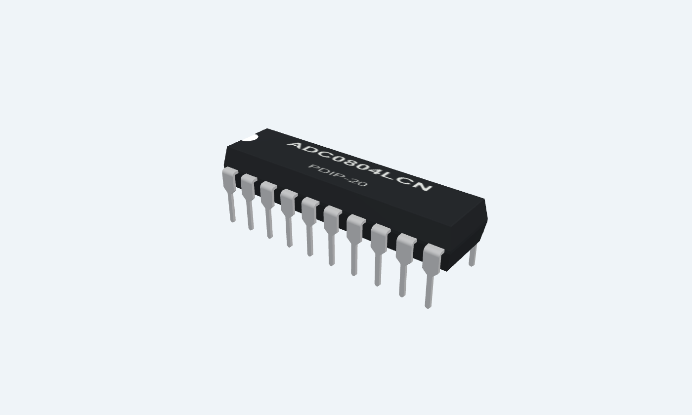
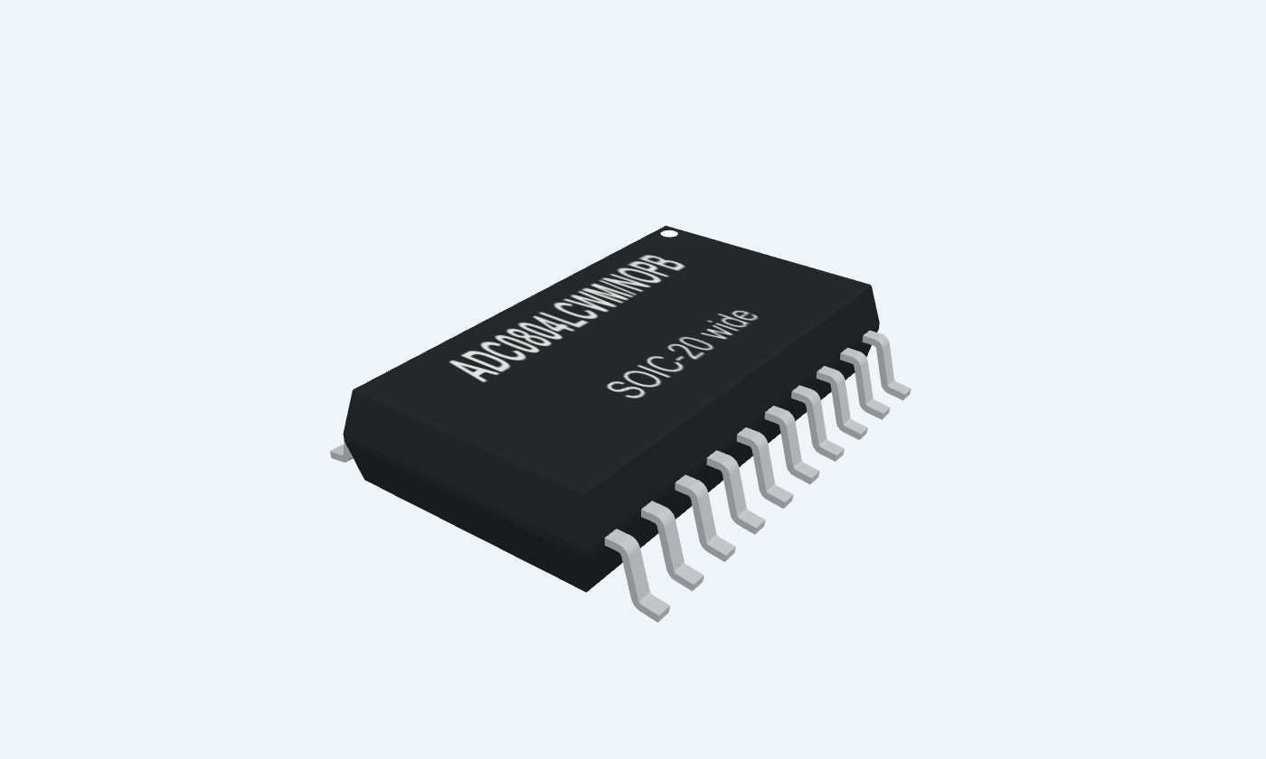
Real View
Measure an analog voltage. Read an eight-bit result.
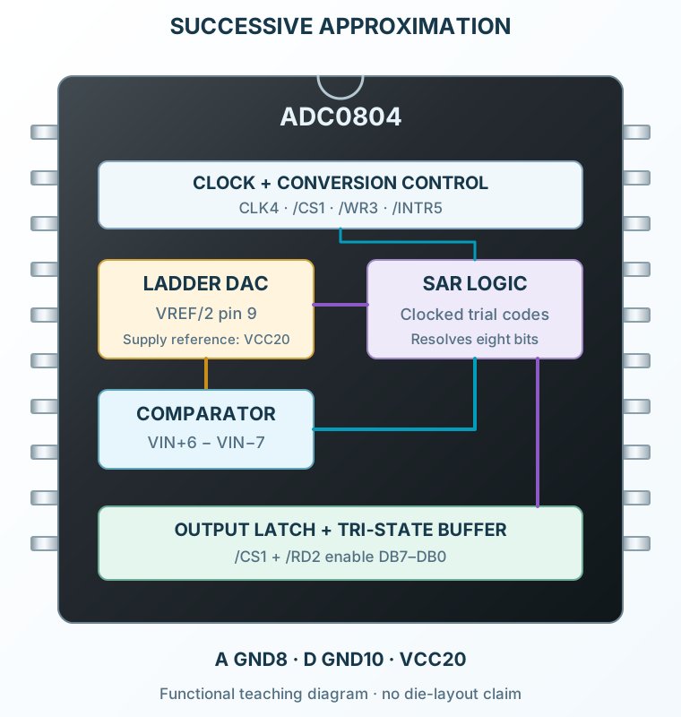
ADC0804 is an 8-bit successive-approximation analog-to-digital converter with a parallel data bus. It measures VIN+ relative to VIN− and stores a code from 0 to 255, which a controller reads using active-LOW chip-select and read signals. A conversion starts with a write strobe, and the interrupt output signals completion. The reference at VREF/2 sets half the input span; leaving it open derives the span from the supply. A nominal 5 V span gives a 19.53125 mV ideal step. This page shows the documented ADC0804LCN PDIP-20 and ADC0804LCWM/NOPB wide SOIC-20 forms. The current TI ordering table lists SOIC variants; the through-hole view remains useful for existing boards. Reference values here use the commercial 0–70°C grades.
Click a lead or use the arrow keys. Top view
Enables the read and conversion-control interface when LOW.
Connect to the controller chip-select output.
With /CS LOW, enables the stored conversion result on DB0–DB7.
Controller read strobe; keep HIGH outside a read.
Outputs are high impedance when /CS or /RD is HIGH.
With /CS LOW, pulse LOW then HIGH to start a conversion.
Controller output; allow the conversion to finish before restarting.
Holding /CS and /WR LOW holds the converter in reset; an early restart does not update the previous result.
External clock input or the RC clock timing node.
Apply a clean 640 kHz, 0–5 V clock for the example.
Use the separate clock thresholds; they differ from /CS, /RD and /WR.
Goes LOW after a completed conversion. Read/start control clears it according to the device timing.
Connect to a controller input.
Wait for completion before reading; follow the manufacturer read/write timing.
Positive input of the differential converter.
Apply a low-impedance, stable 0–5 V signal.
Keep both analog inputs inside the supply rails for the teaching circuit.
Subtracts a fixed offset from VIN+.
Ground for a zero-based measurement.
VIN+ ≤ VIN− produces code zero; this is a unipolar converter, not a signed-output ADC.
Return for the analog ladder and signal reference.
Join to D GND with a low-noise ground layout.
Sets the nominal input span to twice the applied reference voltage.
Leave open for supply-derived reference, or use a suitable low-impedance reference.
For ADC0804LCN/LCWM, input resistance is 1.1 kΩ typical, 0.75 kΩ minimum; account for reference loading.
Return for digital logic and outputs.
Connect to ground and A GND.
Bit 7 of the latched 8-bit conversion result; weight 128.
Connect to the matching controller data input.
Read only with /CS and /RD LOW. High impedance is not logic zero.
Bit 6 of the latched 8-bit conversion result; weight 64.
Connect to the matching controller data input.
Read only with /CS and /RD LOW. High impedance is not logic zero.
Bit 5 of the latched 8-bit conversion result; weight 32.
Connect to the matching controller data input.
Read only with /CS and /RD LOW. High impedance is not logic zero.
Bit 4 of the latched 8-bit conversion result; weight 16.
Connect to the matching controller data input.
Read only with /CS and /RD LOW. High impedance is not logic zero.
Bit 3 of the latched 8-bit conversion result; weight 8.
Connect to the matching controller data input.
Read only with /CS and /RD LOW. High impedance is not logic zero.
Bit 2 of the latched 8-bit conversion result; weight 4.
Connect to the matching controller data input.
Read only with /CS and /RD LOW. High impedance is not logic zero.
Bit 1 of the latched 8-bit conversion result; weight 2.
Connect to the matching controller data input.
Read only with /CS and /RD LOW. High impedance is not logic zero.
Bit 0 of the latched 8-bit conversion result; weight 1.
Connect to the matching controller data input.
Read only with /CS and /RD LOW. High impedance is not logic zero.
Feedback connection for the optional resistor to CLK IN.
Leave open when using the external clock example.
Avoid heavy loading; do not treat this as a general-purpose logic output.
Supplies the converter and sets the default span when VREF/2 is open.
Regulated +5 V with local 100 nF bypass.
Recommended supply section specifies 4.5–5.5 V.
8-bit parallel SAR ADC
A comparator and ladder test successive trial values. The output latch holds the completed code, while /CS and /RD decide whether it drives the data bus.
ADC0804LCN
Key parameters and their test conditions
Follows the selected physical package
Select a pin to open its function, electrical notes and wiring guidance.
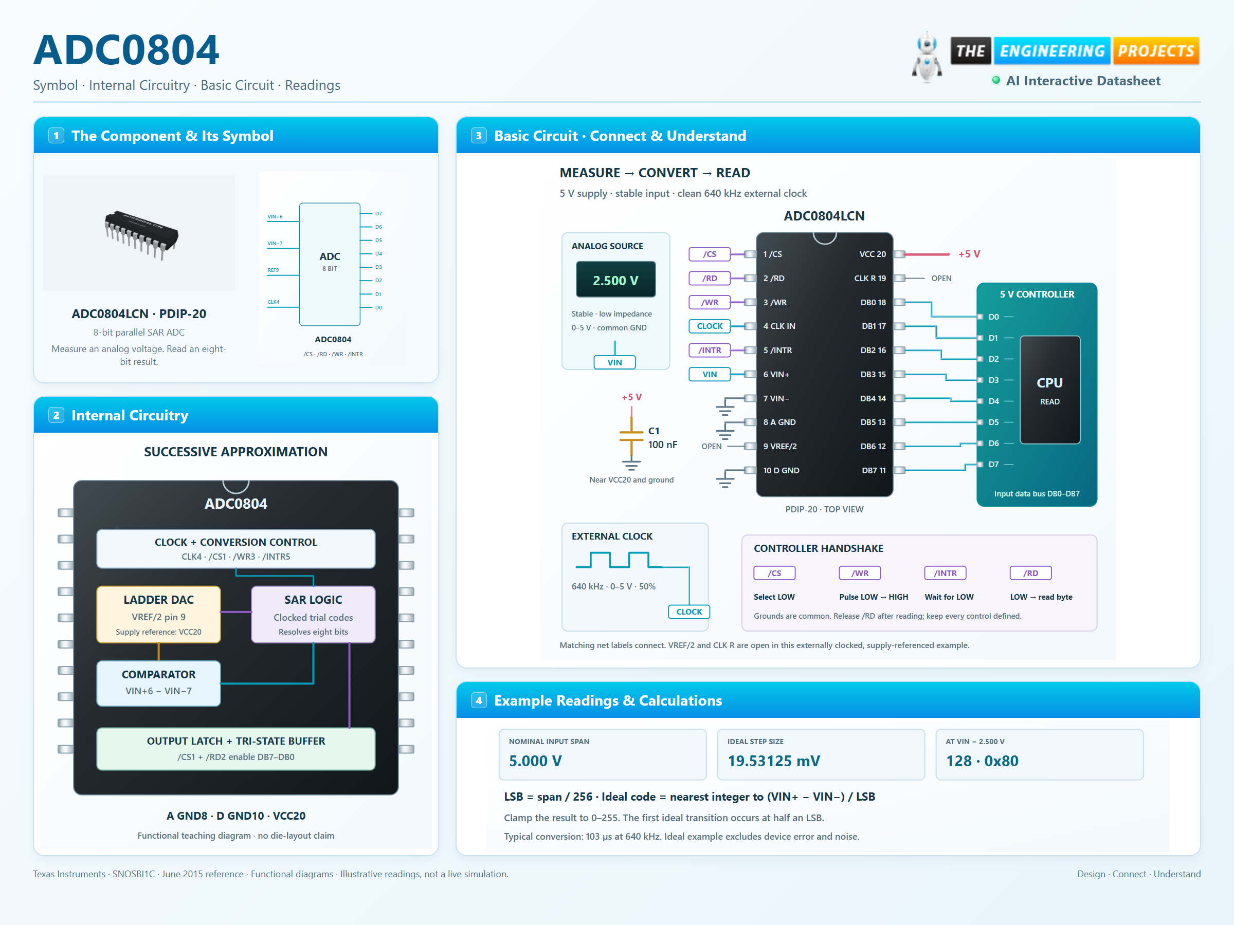
Use VIN− as the offset reference. Twice VREF/2 sets the nominal span; an open VREF/2 uses the supply-derived reference.
With /CS LOW, pulse /WR LOW then HIGH. The SAR compares trial ladder levels and /INTR goes LOW on completion.
Take /RD LOW while /CS is LOW. Read DB7–DB0, then release /RD. The bus returns to high impedance without erasing the stored code.
Resolution, accuracy and conversion time are different limits. Eight bits provide 256 ideal codes; ADC0804 has a specified ±1 LSB total unadjusted error under the stated reference conditions. The teaching explorer shows an ideal transfer, not a timed conversion.
Explore differential input, reference span and the tri-state read bus.
The ideal code updates immediately. Both /CS and /RD must be LOW to enable the eight data outputs. Conversion handshaking is explained in the reference tables.
Ideal static transfer with half-LSB transitions and saturation to codes 0–255. It excludes conversion timing, analog noise and device error. Code-centre voltage is a nominal reconstructed value, not the exact measured input. Reference/2 is bounded to 0.5–2.5 V here for exploration.
Select a pin to explore its function and connection.
| Pin | Signal | Type | Function |
|---|---|---|---|
| /CS | Active-LOW chip select | Enables the read and conversion-control interface when LOW. | |
| /RD | Active-LOW read | With /CS LOW, enables the stored conversion result on DB0–DB7. | |
| /WR | Active-LOW conversion strobe | With /CS LOW, pulse LOW then HIGH to start a conversion. | |
| CLK IN | Clock input | External clock input or the RC clock timing node. | |
| /INTR | Active-LOW completion | Goes LOW after a completed conversion. Read/start control clears it according to the device timing. | |
| VIN+ | Positive analog input | Positive input of the differential converter. | |
| VIN− | Negative analog input | Subtracts a fixed offset from VIN+. | |
| A GND | Analog ground | Return for the analog ladder and signal reference. | |
| VREF/2 | Half-span reference | Sets the nominal input span to twice the applied reference voltage. | |
| D GND | Digital ground | Return for digital logic and outputs. | |
| DB7 | Tri-state data output | Bit 7 of the latched 8-bit conversion result; weight 128. | |
| DB6 | Tri-state data output | Bit 6 of the latched 8-bit conversion result; weight 64. | |
| DB5 | Tri-state data output | Bit 5 of the latched 8-bit conversion result; weight 32. | |
| DB4 | Tri-state data output | Bit 4 of the latched 8-bit conversion result; weight 16. | |
| DB3 | Tri-state data output | Bit 3 of the latched 8-bit conversion result; weight 8. | |
| DB2 | Tri-state data output | Bit 2 of the latched 8-bit conversion result; weight 4. | |
| DB1 | Tri-state data output | Bit 1 of the latched 8-bit conversion result; weight 2. | |
| DB0 | Tri-state data output | Bit 0 of the latched 8-bit conversion result; weight 1. | |
| CLK R | RC clock feedback output | Feedback connection for the optional resistor to CLK IN. | |
| VCC | Positive supply and ladder reference | Supplies the converter and sets the default span when VREF/2 is open. |
No pins match. Try a signal name or choose All pins.
ADC0804LCN / ADC0804LCWM
| Parameter | Value | Conditions / notes |
|---|---|---|
| Recommended supply | 4.5–5.5 V | Recommended operating conditions section; 5 V example |
| Commercial temperature | 0–70°C | LCN and LCWM grades |
| Differential input | VIN+ − VIN− | Both pins must stay within the permitted common-mode range |
| Analog pin range | GND − 0.05 to VCC + 0.05 V | Manufacturer rating; example stays between GND and VCC |
| Reference span | 2 × VREF/2 | Open reference pin gives a supply-derived span |
| Negative differential input | Code 0 | Unipolar result, not signed arithmetic |
No specifications match. Try a parameter name or a unit.
The legacy operating-ratings table also lists 6.3 V; this page follows the recommended 4.5–5.5 V supply section.
5 V · 640 kHz unless noted
| Parameter | Value | Conditions / notes |
|---|---|---|
| Resolution | 8 bits / 256 codes | Output codes 0–255 |
| Ideal LSB at 5 V span | 19.53125 mV | 5 V / 256 |
| Total unadjusted error | ±1 LSB | ADC0804; VREF/2 = 2.500 V |
| Conversion time | 103 µs typical; 114 µs maximum | Specified temperature range |
| Clock periods per conversion | 66 typical; 73 maximum | Asynchronous start timing included |
| Clock range | 100–1460 kHz | Accuracy specified at 640 kHz |
| Clock duty cycle | 40–60% | At specified clock conditions |
No specifications match. Try a parameter name or a unit.
Do not substitute ADC0801 or ADC0802 accuracy grades. Faster clocks can reduce accuracy.
Active-LOW parallel interface
| Parameter | Value | Conditions / notes |
|---|---|---|
| /CS HIGH | Data bus Hi-Z | Read and conversion-control interface not selected |
| /CS LOW, /WR LOW | Reset/start request | Hold for at least the required strobe width |
| /WR rising with /CS LOW | Start conversion | Wait for /INTR LOW |
| /CS LOW, /RD LOW | Drive stored DB7–DB0 | Read after conversion completion |
| /RD HIGH or /CS HIGH | Data bus Hi-Z | Stored result remains latched |
| Minimum /WR LOW pulse | 100 ns | /CS LOW |
| Read access delay | 135 ns typical; 200 ns maximum | CL = 100 pF |
| Data release to Hi-Z | 125 ns typical; 200 ns maximum | CL = 10 pF; RL = 10 kΩ |
No specifications match. Try a parameter name or a unit.
Restarting before completion preserves the previous result. The explorer displays settled transfer and bus-enable behavior only.
Manufacturer test conditions
| Parameter | Value | Conditions / notes |
|---|---|---|
| Control input HIGH / LOW | ≥ 2.0 V / ≤ 0.8 V | Excludes CLK IN; see specified supply test conditions |
| CLK IN rising threshold | 2.7 / 3.1 / 3.5 V | Minimum / typical / maximum |
| CLK IN falling threshold | 1.5 / 1.8 / 2.1 V | Minimum / typical / maximum |
| Data-output LOW | ≤ 0.4 V at 1.6 mA | VCC = 4.75 V |
| Output HIGH | ≥ 2.4 V at −360 µA | ≥ 4.5 V at −10 µA; VCC = 4.75 V |
| Reference/2 resistance | 0.75 kΩ minimum; 1.1 kΩ typical | LCN/LCWM reference loading |
| Supply current | 1.9 mA typical; 2.5 mA maximum | 25°C, 640 kHz, VREF/2 open, /CS = 5 V |
No specifications match. Try a parameter name or a unit.
Logic output voltages depend on load; do not assume every HIGH equals VCC.
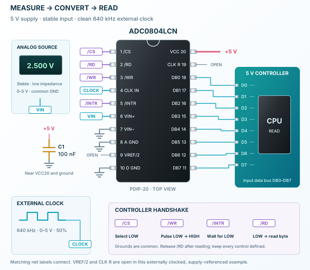
External clock · supply-derived span
| Parameter | Value | Conditions / notes |
|---|---|---|
| Analog source | Stable 0–5 V into VIN+6 | Low impedance; VIN−7 to GND |
| Reference pin9 | Open | Uses supply-derived reference; no external reference is shown |
| External clock | 640 kHz into CLK IN4 | 0–5 V, 50% duty; CLK R19 open |
| Control signals | /CS1, /RD2, /WR3 | Controller outputs with defined idle states |
| Completion signal | /INTR5 | Controller input |
| Data byte | DB0 pin18 through DB7 pin11 | Controller input bus; bit order matters |
| Ground and bypass | A GND8 / D GND10 / VCC20 | Common ground; 100 nF close to supply pins |
No specifications match. Try a parameter name or a unit.
For each measurement, assert /CS, pulse /WR, wait for /INTR LOW, then read with /RD LOW. This is not the separate free-running connection.
Stress limits, not operating settings
| Parameter | Value | Conditions / notes |
|---|---|---|
| Supply voltage | 6.5 V maximum | Use recommended supply for operation |
| Logic control inputs | −0.3 to +18 V | Stress rating; not the example drive voltage |
| Other input/output pins | −0.3 to VCC + 0.3 V | Includes analog inputs |
| Package dissipation at 25°C | 875 mW | Thermal conditions and derating apply |
| Storage temperature | −65 to +150°C | Unpowered storage |
No specifications match. Try a parameter name or a unit.
Stay within recommended operating and input conditions during normal use.
Convert conditioned analog sensor voltages into a parallel byte.
Manufacturer application guideConnect an 8-bit microprocessor bus with chip-select, read, write and interrupt timing.
Manufacturer application guideExplore resolution, offset and saturation while keeping both analog inputs in range.
Manufacturer application guideFind ADC0804 in the Components Library to place its schematic symbol and connect its pins.
Reference page · circuit simulation model not yet availableOpen ProTech