BC547Small-signal NPN transistor
Amplify a small signal. Switch a modest load.
BC547 is a small-signal NPN bipolar transistor for amplification and modest switching loads. Its base-emitter junction controls the collector current; an external bias network or load determines whether it operates as an amplifier or a saturated switch. This page selects Diotec’s BC547BBK: B gain grade, bulk straight-lead TO-92 package, 1.27 mm pitch. Viewed from the flat front with the leads down, the terminals are collector, base and emitter. The A, B and C gain groups have different specified DC-gain ranges. A physical 5 V LED example shows separate base and load resistors. The calculated values illustrate operation and use stated voltage assumptions. BC847 is a separately named SMD relative, and other manufacturers’ BC547 limits must not be substituted into this selected reference.
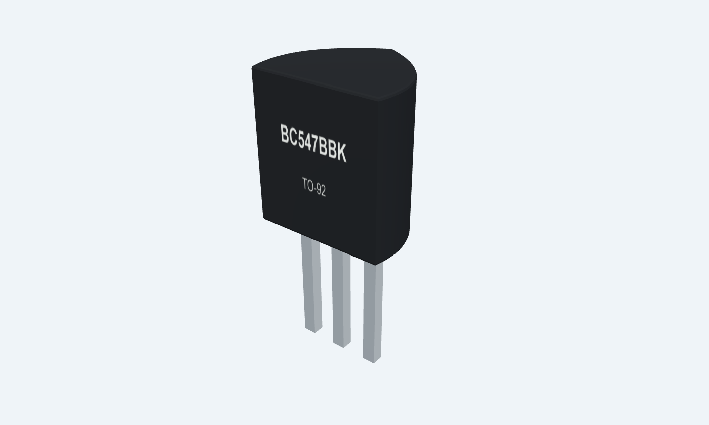

Collector / loadBase / controlEmitter / return
BC547BBKTO-92Front view · flat face · C1, B2, E3
Click a lead or use the arrow keys. Front view · flat face · C1, B2, E3
PIN 1 · Collector / load
CollectorC
Function
Receives the switched load current.
How to connect
Connect to the LED cathode in the low-side switch example.
Electrical note
The selected Diotec BC547BBK is C–B–E when viewed from the flat front with leads down.
PIN 2 · Base / control
BaseB
Function
Controls the collector current through the base-emitter junction.
How to connect
Drive through 4.7 kΩ in the example; use 100 kΩ from base to emitter.
Electrical note
Use the gain grade at its stated test conditions. Saturation requires a separate base-current budget.
PIN 3 · Emitter / return
EmitterE
Function
Common return for the NPN low-side switch.
How to connect
Connect to the controller and load-supply ground.
Electrical note
Do not swap this with collector pin 1; the package resembles transistors with different pinouts.
At a glance
Small-signal NPN transistor
A B-grade BC547 has a specified active-region gain range at one test point. A saturated switch instead needs enough base current for its load and a separate power check.
45 V · absolute VCEOCollector voltage
100 mA · absoluteDC collector limit
200–450 VCE 5 V · IC 2 mAB-grade DC gain
150 °C · maximumJunction limit
Operating profile
BC547BBK
Selected device
Key parameters and their test conditions
- Reference
- Diotec BC546xBK–BC549xBKConditions / notes: Version 2009-12-03
- Selected part
- BC547BBKConditions / notes: B gain group; bulk straight-lead package
- Package
- TO-92 · 1.27 mm lead pitchConditions / notes: Approximately 4.6 mm body width and height
- Front-view pinout
- 1 C · 2 B · 3 EConditions / notes: Flat face towards you, leads down
- Related SMD family
- BC847Conditions / notes: A separate part number, not an assumed BC547 package switch
- Complementary family
- BC556–BC559Conditions / notes: BC557 is the corresponding PNP voltage class
Package details
Follows the selected physical package
- Manufacturer
- Diotec Semiconductor
- Part number
- BC547BBK
- Package
- TO-92
- Connections
- 3 pins
- Mounting
- Through-hole
- Lead pitch
- 1.27 mm · straight leads
- Package code
- BK
- Thermal reference
- 500 mW rating assumes leads held at ambient temperature 2 mm from the case
Connections by function
Select a pin to open its function, electrical notes and wiring guidance.
Collector / load1 pins
Base / control1 pins
Emitter / return1 pins
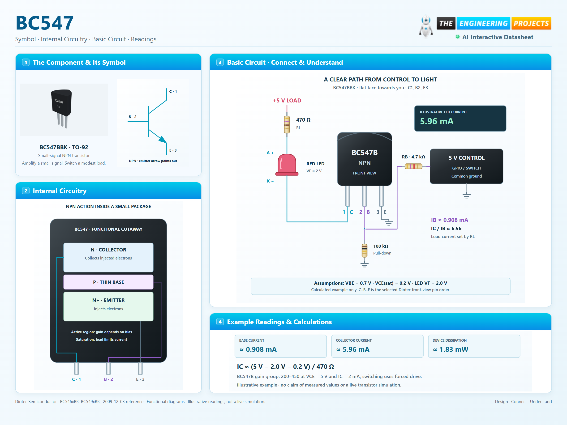
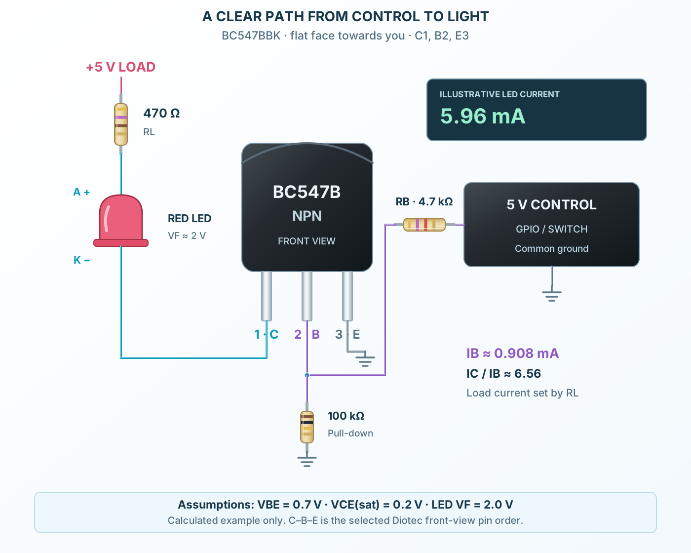
Bias or switch
Choose forward-active bias for amplification or deliberate saturation for a switch.
Limit both current paths
The base resistor protects the control output; the LED resistor controls load current.
Check the exact part
This front-view C–B–E pinout belongs to the reviewed straight-lead Diotec package.
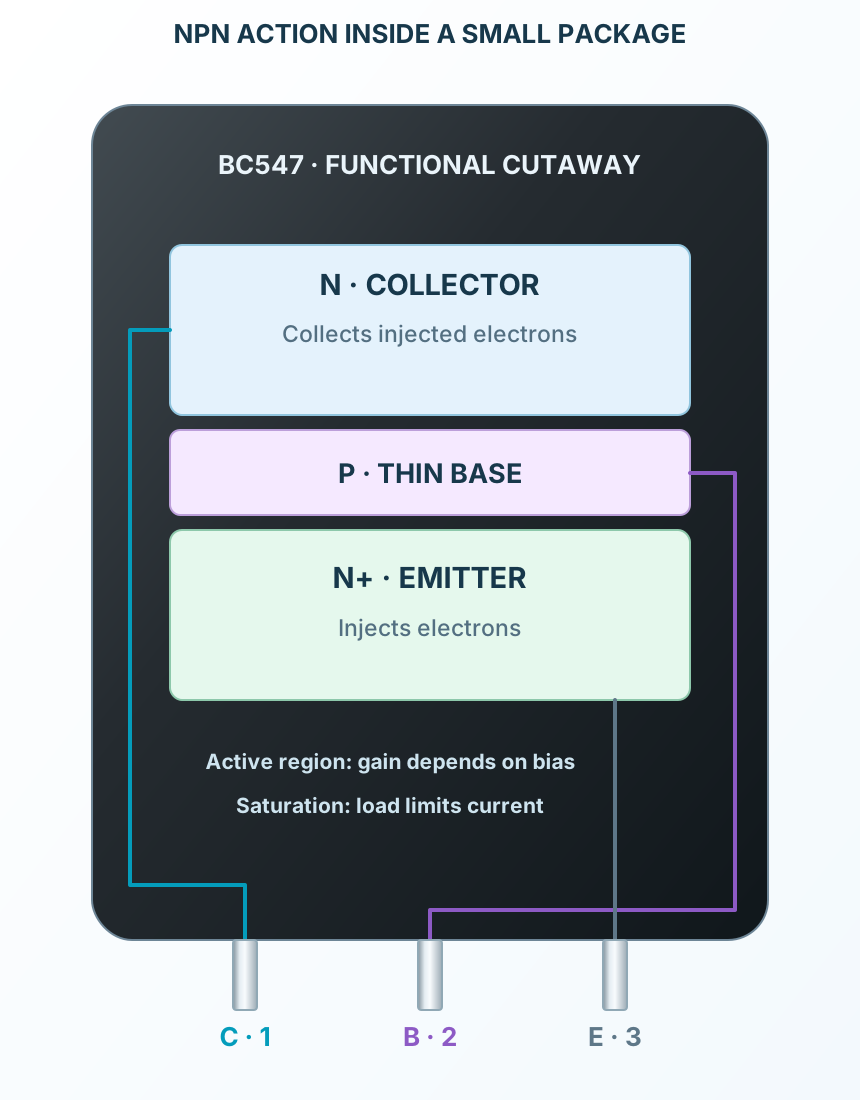
With a 4.7 kΩ base resistor and 100 kΩ pull-down, the example supplies about 0.908 mA of base current. Its 470 Ω LED resistor sets about 5.96 mA using the stated voltage assumptions.
Pin reference
Select a pin to explore its function and connection.
3 pins
| Pin | Signal | Type | Function |
|---|---|---|---|
| C | Collector | Receives the switched load current. | |
| B | Base | Controls the collector current through the base-emitter junction. | |
| E | Emitter | Common return for the NPN low-side switch. |
No pins match. Try a signal name or choose All pins.
Selected device
Manufacturer and package scope
Manufacturer specifications 6 parameters
| Parameter | Value | Conditions / notes |
|---|---|---|
| Reference | Diotec BC546xBK–BC549xBK | Version 2009-12-03 |
| Selected part | BC547BBK | B gain group; bulk straight-lead package |
| Package | TO-92 · 1.27 mm lead pitch | Approximately 4.6 mm body width and height |
| Front-view pinout | 1 C · 2 B · 3 E | Flat face towards you, leads down |
| Related SMD family | BC847 | A separate part number, not an assumed BC547 package switch |
| Complementary family | BC556–BC559 | BC557 is the corresponding PNP voltage class |
No specifications match. Try a parameter name or a unit.
Datasheet version and manufacturer are explicit so later revisions can be reviewed independently.
Absolute maximum ratings
TA = 25°C · selected BC547 family
Manufacturer specifications 7 parameters
| Parameter | Value | Conditions / notes |
|---|---|---|
| Collector-emitter voltage | 45 V with base open | VCEO |
| Collector-emitter voltage | 50 V with base-emitter shorted | VCES |
| Collector-base voltage | 50 V with emitter open | VCBO |
| Emitter-base voltage | 5 V with collector open | Reverse-voltage stress limit |
| DC / peak collector current | 100 mA / 200 mA | Thermal and pulse constraints also apply |
| Power dissipation | 500 mW | Leads held at ambient temperature 2 mm from case |
| Junction / storage range | −55 to +150°C | Absolute limits from this BK reference |
No specifications match. Try a parameter name or a unit.
These stress ratings are not recommended continuous operating targets.
A, B and C gain groups
VCE = 5 V · IC = 2 mA · junction at 25°C
Manufacturer specifications 6 parameters
| Parameter | Value | Conditions / notes |
|---|---|---|
| Group A | hFE 110–220 | A separate gain selection |
| Group B | hFE 200–450 | The BC547BBK selected here |
| Group C | hFE 420–800 | A separate gain selection |
| Group B at IC = 10 µA | 150 typical | VCE = 5 V; not a guaranteed minimum |
| Group B at IC = 100 mA | 200 typical | VCE = 5 V; pulsed characteristic |
| Small-signal gain hfe, group B | 330 typical | VCE = 5 V, IC = 2 mA, f = 1 kHz |
No specifications match. Try a parameter name or a unit.
DC hFE, small-signal hfe and forced saturation current ratio describe different conditions.
Electrical test points
Typical and maximum values are kept separate
Manufacturer specifications 6 parameters
| Parameter | Value | Conditions / notes |
|---|---|---|
| VCE(sat), IC 10 mA / IB 0.5 mA | 80 mV typical; 200 mV maximum | Pulsed test: 300 µs, duty ≤ 2% |
| VCE(sat), IC 100 mA / IB 5 mA | 200 mV typical; 600 mV maximum | Pulsed test: 300 µs, duty ≤ 2% |
| VBE at IC = 2 mA | 580 / 660 / 700 mV | Minimum / typical / maximum; VCE = 5 V |
| Collector-emitter leakage | 0.2 nA typical; 15 nA maximum | VCE = 50 V; B–E short; junction 25°C |
| Leakage at junction 125°C | 4 µA maximum | VCE = 50 V; B–E short |
| Transition frequency fT | 300 MHz typical | VCE = 5 V; IC = 10 mA; f = 100 MHz |
No specifications match. Try a parameter name or a unit.
The 300 MHz figure is typical small-signal behavior, not a guaranteed digital switching frequency.
Small-signal and noise data
Manufacturer test conditions
Manufacturer specifications 6 parameters
| Parameter | Value | Conditions / notes |
|---|---|---|
| Group B input impedance hie | 3.2–8.5 kΩ | VCE = 5 V; IC = 2 mA; f = 1 kHz |
| Collector-base capacitance | 3.5 pF typical; 6 pF maximum | VCB = 10 V; f = 1 MHz; emitter current zero |
| Emitter-base capacitance | 9 pF typical | VEB = 0.5 V; f = 1 MHz; collector current zero |
| BC547 noise figure | 2 dB typical; 10 dB maximum | VCE 5 V; IC 200 µA; RG 2 kΩ; 1 kHz; bandwidth 200 Hz |
| Thermal resistance | Less than 200 K/W in the stated setup | Leads at ambient temperature 2 mm from the case |
| Practical amplifier bias | Keep collector-emitter headroom | Avoid cutoff and saturation over the intended signal swing |
No specifications match. Try a parameter name or a unit.
Noise and gain depend on bias and frequency. Do not substitute a low-noise family’s limits.
5 V LED switch
Pin numbers match the pictured front view
Manufacturer specifications 6 parameters
| Parameter | Value | Conditions / notes |
|---|---|---|
| Collector pin 1 | LED cathode | LED anode through 470 Ω to +5 V |
| Base pin 2 | Control through 4.7 kΩ | 100 kΩ pull-down from base to emitter |
| Emitter pin 3 | Common GND | Connect controller and load supply returns |
| Illustrative assumptions | VBE 0.7 V; VCE(sat) 0.2 V; LED 2.0 V | Example values, not guaranteed test results |
| Control resistor current | 0.915 mA | (5 − 0.7) / 4.7 kΩ |
| Base current after pull-down | 0.908 mA | Subtract 7 µA flowing in 100 kΩ |
No specifications match. Try a parameter name or a unit.
The example uses a small LED load, well below the absolute collector-current limit.
Example current and power
Nominal teaching arithmetic
Manufacturer specifications 7 parameters
| Parameter | Value | Conditions / notes |
|---|---|---|
| Collector / LED current | 5.96 mA | (5 − 2.0 − 0.2) / 470 Ω |
| Forced current ratio | Approximately 6.56 | Collector current divided by base current |
| Collector-emitter dissipation | Approximately 1.19 mW | 0.2 V × 5.96 mA |
| Base-emitter contribution | Approximately 0.636 mW | 0.7 V × 0.908 mA |
| Total transistor dissipation | Approximately 1.83 mW | Sum of both electrical contributions |
| Load-resistor dissipation | Approximately 16.7 mW | I² × 470 Ω |
| Inductive loads | Require flyback protection | Do not replace the LED with a coil without revising the circuit |
No specifications match. Try a parameter name or a unit.
These are explanatory calculations, not live readings or a simulator model.
Signal amplification
Use controlled bias and an appropriate load for small analog signals.
Manufacturer application guideIndicator switching
Switch a small LED load with separate base and LED resistors.
Manufacturer application guideInverting interfaces
Use a pulled-up collector where voltage and current limits allow.
Manufacturer application guideTake it into ProTech
Find BC547 in the Components Library to place its schematic symbol and connect its pins.
Reference page · circuit simulation model not yet availableOpen ProTech