BD139Medium-power NPN transistor
Control a larger load. Keep the thermal path clear.
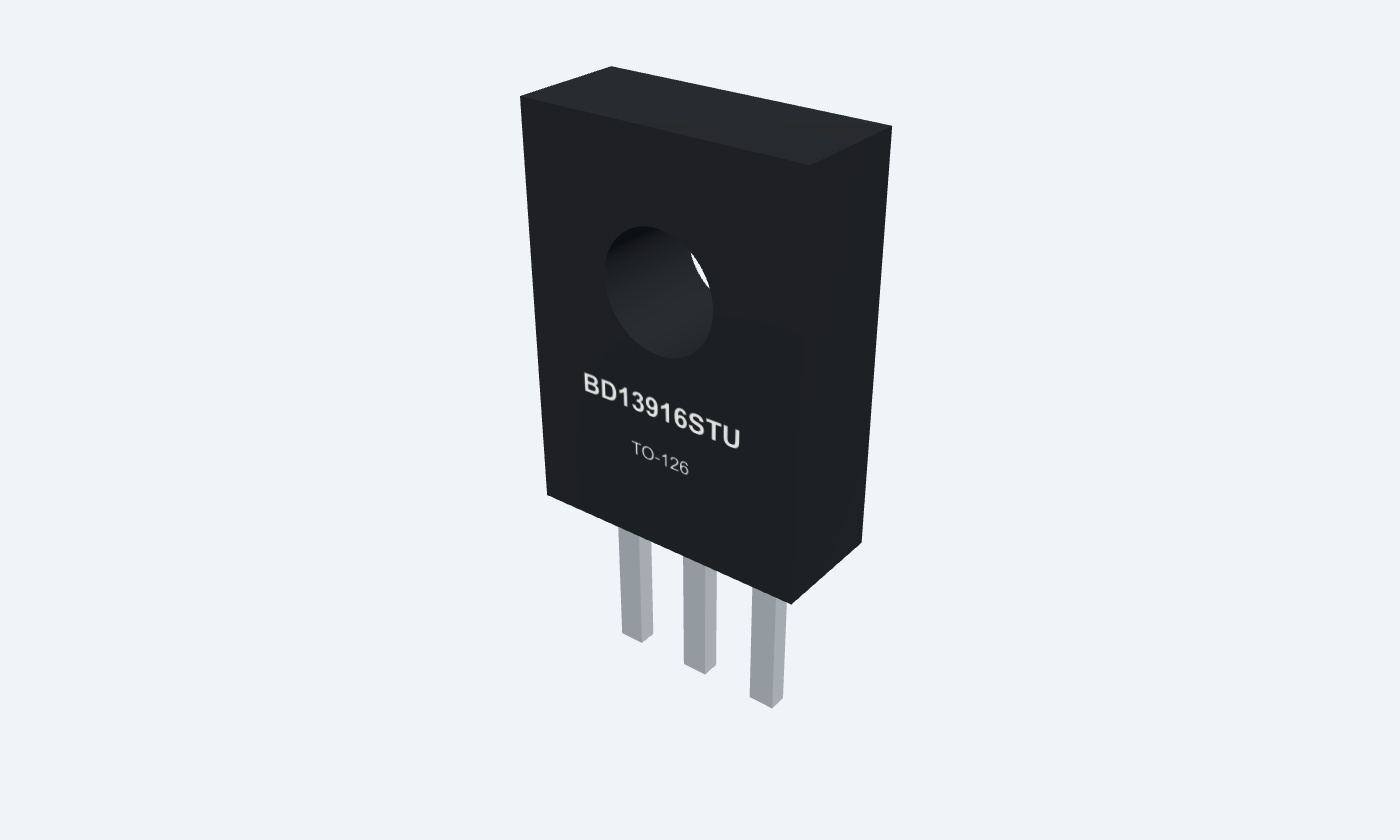
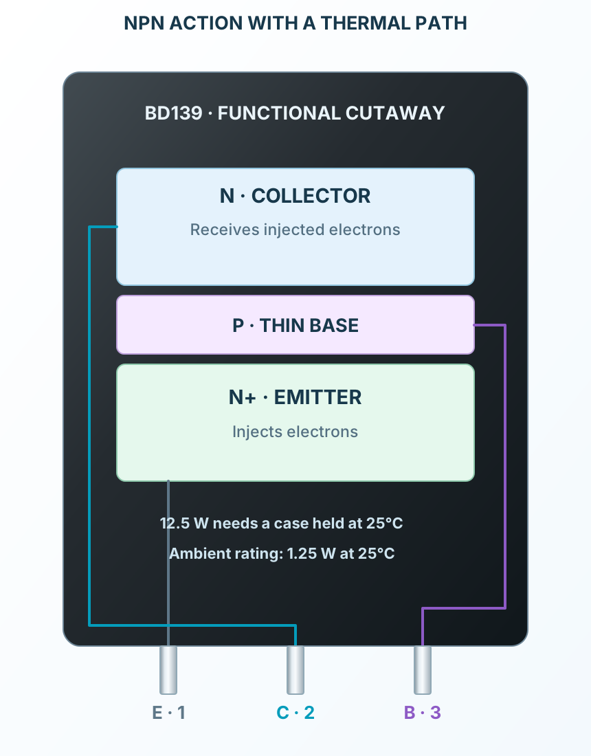
BD139 is an NPN transistor for medium-power amplification and switching. A small base current controls the collector path, while the external circuit sets the load current and the heat that must leave the package. This page selects onsemi BD13916STU in TO-126. With the marked front facing you and the leads pointing down, its terminals are emitter, collector and base. The original package illustration and PCB pattern follow the manufacturer’s 2.29 mm lead pitch. The 12.5 W figure requires the case to be held at 25°C; the separate ambient rating is 1.25 W at 25°C. A modest resistor-load example explains base drive and power without suggesting that the absolute ratings are ordinary operating targets.

Emitter / returnCollector / loadBase / control
BD13916STUTO-126Front view · E1, C2, B3
Click a lead or use the arrow keys. Front view · E1, C2, B3
PIN 1 · Emitter / return
EmitterE
Function
Return terminal of the NPN switch.
How to connect
Join the control and load grounds.
Electrical note
Front-facing TO-126, leads down: E1, C2, B3.
PIN 2 · Collector / load
CollectorC
Function
Connects to the controlled load.
How to connect
Use the 100 Ω resistor load in the pictured circuit.
Electrical note
The collector current and device dissipation must both remain within limits.
PIN 3 · Base / control
BaseB
Function
Controls the collector current.
How to connect
Drive through 1 kΩ; connect 10 kΩ from base to emitter.
Electrical note
Saturation requires explicit base current; do not assume active-region hFE remains constant.
At a glance
Medium-power NPN transistor
Collector-current capability alone is not enough: check base drive, collector voltage, device power and the actual thermal path together.
80 V · absolute VCEOCollector voltage
1.5 A · absoluteDC collector limit
12.5 W · TC = 25°CCase-cooled power
150 °C · maximumJunction limit
Operating profile
BD13916STU
Selected reference
Key parameters and their test conditions
- Selected device
- onsemi BD13916STUConditions / notes: TO-126; rail packing; marking BD139-16
- Electrical reference
- BD139/D Rev. 3Conditions / notes: April 2026
- Mechanical reference
- CASE 340AS, Issue OConditions / notes: 30 September 2016; drawing 98AON13817G
- Front-view terminals
- 1 E · 2 C · 3 BConditions / notes: Marked face forward, leads down
- Lead pitch
- 2.29 mmConditions / notes: Body nominally 8 × 11 × 3.25 mm
- Gain selection
- Use the current published 40–250 test-point rangeConditions / notes: Rev. 3 removed the older hFE classification table
Package details
Follows the selected physical package
- Manufacturer
- onsemi
- Part number
- BD13916STU
- Package
- TO-126
- Connections
- 3 pins
- Mounting
- Through-hole
- Lead pitch
- 2.29 mm
- Package code
- 340AS
- Thermal reference
- 12.5 W at case 25°C; 1.25 W at ambient 25°C
Connections by function
Select a pin to open its function, electrical notes and wiring guidance.
Emitter / return1 pins
Collector / load1 pins
Base / control1 pins
Choose the operating region
Forward-active operation supports amplification; deliberate saturation supports switching.
Budget base current
Include the pull-down current and the capability of the control output.
Provide a thermal path
Use junction-to-case or junction-to-ambient resistance for the appropriate mounting conditions.
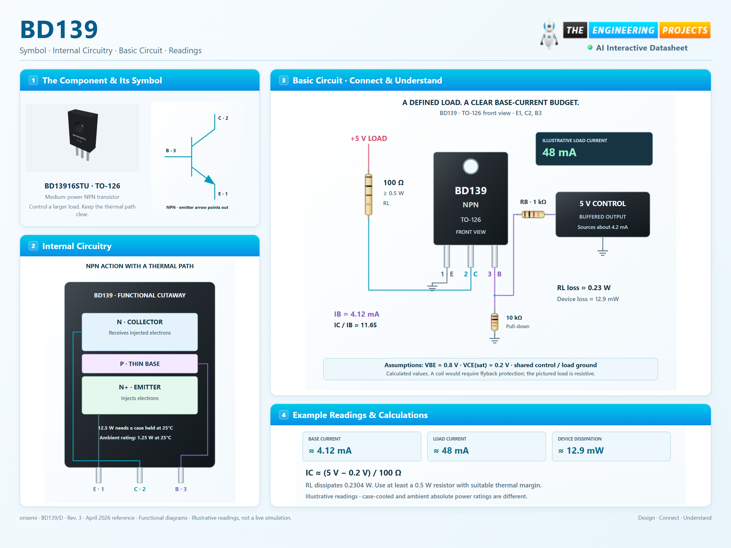
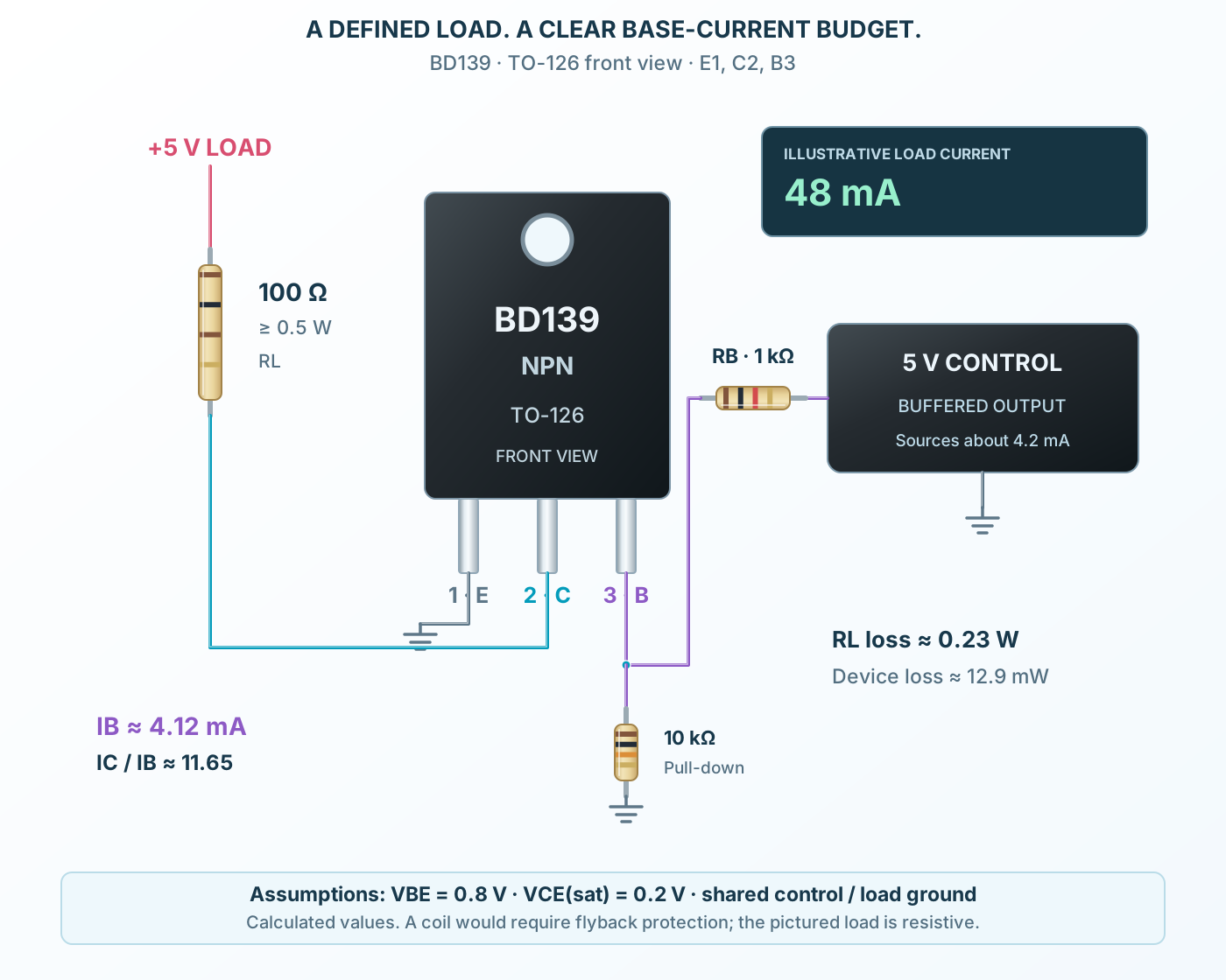
With the stated 0.8 V base and 0.2 V saturation assumptions, a 1 kΩ drive resistor supplies 4.12 mA after the pull-down. A 100 Ω load draws 48 mA and dissipates about 0.23 W.
Pin reference
Select a pin to explore its function and connection.
3 pins
| Pin | Signal | Type | Function |
|---|---|---|---|
| E | Emitter | Return terminal of the NPN switch. | |
| C | Collector | Connects to the controlled load. | |
| B | Base | Controls the collector current. |
No pins match. Try a signal name or choose All pins.
Selected reference
Manufacturer, ordering and package scope
Manufacturer specifications 6 parameters
| Parameter | Value | Conditions / notes |
|---|---|---|
| Selected device | onsemi BD13916STU | TO-126; rail packing; marking BD139-16 |
| Electrical reference | BD139/D Rev. 3 | April 2026 |
| Mechanical reference | CASE 340AS, Issue O | 30 September 2016; drawing 98AON13817G |
| Front-view terminals | 1 E · 2 C · 3 B | Marked face forward, leads down |
| Lead pitch | 2.29 mm | Body nominally 8 × 11 × 3.25 mm |
| Gain selection | Use the current published 40–250 test-point range | Rev. 3 removed the older hFE classification table |
No specifications match. Try a parameter name or a unit.
This page does not infer a tighter gain guarantee from the ordering suffix.
Absolute maximum ratings
Stress limits at the stated temperature
Manufacturer specifications 7 parameters
| Parameter | Value | Conditions / notes |
|---|---|---|
| Collector-emitter / collector-base | 80 V / 80 V | VCEO / VCBO |
| Emitter-base reverse voltage | 5 V | VEBO |
| DC / pulse collector current | 1.5 A / 3 A | Pulse and thermal constraints also apply |
| Base current | 0.5 A | Absolute maximum |
| Dissipation at case 25°C | 12.5 W | Requires the specified case temperature |
| Dissipation at ambient 25°C | 1.25 W | A different thermal boundary condition |
| Junction maximum | 150°C | Storage −55 to +150°C |
No specifications match. Try a parameter name or a unit.
Simultaneously applying the individual maximum ratings is not a valid design method.
Current gain
Forward-active test conditions
Manufacturer specifications 4 parameters
| Parameter | Value | Conditions / notes |
|---|---|---|
| IC = 5 mA, VCE = 2 V | hFE ≥ 25 | Minimum |
| IC = 150 mA, VCE = 2 V | hFE 40–250 | Minimum and maximum |
| IC = 500 mA, VCE = 2 V | hFE ≥ 25 | Minimum |
| Switching calculation | Use a forced IC / IB ratio | Active-region gain is not a saturation guarantee |
No specifications match. Try a parameter name or a unit.
Use the onsemi current revision rather than another manufacturer’s selected gain bins.
Electrical characteristics
Guaranteed values at defined operating points
Manufacturer specifications 6 parameters
| Parameter | Value | Conditions / notes |
|---|---|---|
| Collector-emitter saturation | VCE(sat) ≤ 0.5 V | IC = 500 mA; IB = 50 mA |
| Base-emitter on voltage | VBE(on) ≤ 1 V | IC = 500 mA; VCE = 2 V |
| Collector cutoff current | ICBO ≤ 0.1 µA | VCB = 30 V; IE = 0 |
| Emitter cutoff current | IEBO ≤ 10 µA | VEB = 5 V; IC = 0 |
| Breakdown VCEO | At least 80 V | IC = 30 mA; IB = 0 |
| Breakdown VCBO | At least 80 V | IC = 100 µA; IE = 0 |
No specifications match. Try a parameter name or a unit.
The illustrative 0.2 V saturation value in the example is not substituted for the manufacturer’s 0.5 V maximum test point.
Thermal design
The cooling condition changes allowable power
Manufacturer specifications 6 parameters
| Parameter | Value | Conditions / notes |
|---|---|---|
| Junction-to-case | RθJC ≤ 10°C/W | Case temperature must be known |
| Junction-to-ambient | RθJA ≤ 100°C/W | Use the manufacturer’s stated mounting condition |
| Case-based estimate | TJ ≈ TC + P × RθJC | Include interface and heatsink resistance when finding TC |
| Ambient-based estimate | TJ ≈ TA + P × RθJA | PCB and enclosure conditions can change the result |
| Example device loss | Approximately 12.9 mW | Includes collector and base contributions |
| Mounting | Check insulation and clearances | The 3D model is an illustration, not manufacturing CAD |
No specifications match. Try a parameter name or a unit.
Keep margin below 150°C and check transient operation separately.
5 V resistor-load switch
An explicit, modest load and base-drive budget
Manufacturer specifications 6 parameters
| Parameter | Value | Conditions / notes |
|---|---|---|
| Collector pin 2 | 100 Ω load to +5 V | Use a resistor rated at least 0.5 W |
| Base pin 3 | 5 V buffered control through 1 kΩ | Control must source approximately 4.2 mA |
| Emitter pin 1 | Common ground | Share the controller and load return |
| Base-emitter pull-down | 10 kΩ | Ensures a defined off state |
| Assumed junction voltages | VBE = 0.8 V; VCE(sat) = 0.2 V | Illustrative values, not guaranteed readings |
| Inductive loads | Require a suitable flyback clamp | The pictured resistor is not an inductive load |
No specifications match. Try a parameter name or a unit.
Use a buffered control source if the MCU cannot provide the required current.
Example calculations
Teaching arithmetic using the stated assumptions
Manufacturer specifications 7 parameters
| Parameter | Value | Conditions / notes |
|---|---|---|
| Drive-resistor current | 4.20 mA | (5 − 0.8) / 1 kΩ |
| Pull-down current | 0.08 mA | 0.8 / 10 kΩ |
| Base current | 4.12 mA | Drive current minus pull-down current |
| Collector current | 48 mA | (5 − 0.2) / 100 Ω |
| Forced current ratio | Approximately 11.65 | 48 mA / 4.12 mA |
| Transistor dissipation | Approximately 12.9 mW | 0.2 × 0.048 + 0.8 × 0.00412 |
| Load-resistor dissipation | 0.2304 W | (0.048 A)² × 100 Ω |
No specifications match. Try a parameter name or a unit.
Calculated values explain the circuit; they are not measured values or a timed simulation.
Driver stages
Drive moderate loads with explicit current and thermal margins.
Manufacturer application guideAnalog amplification
Bias in the forward-active region and verify signal headroom.
Manufacturer application guideComplementary circuits
BD140 is the related PNP family; verify its separate reference.
Manufacturer application guideTake it into ProTech
Find BD139 in the Components Library to place its schematic symbol and connect its pins.
Reference page · circuit simulation model not yet availableOpen ProTech