Real View
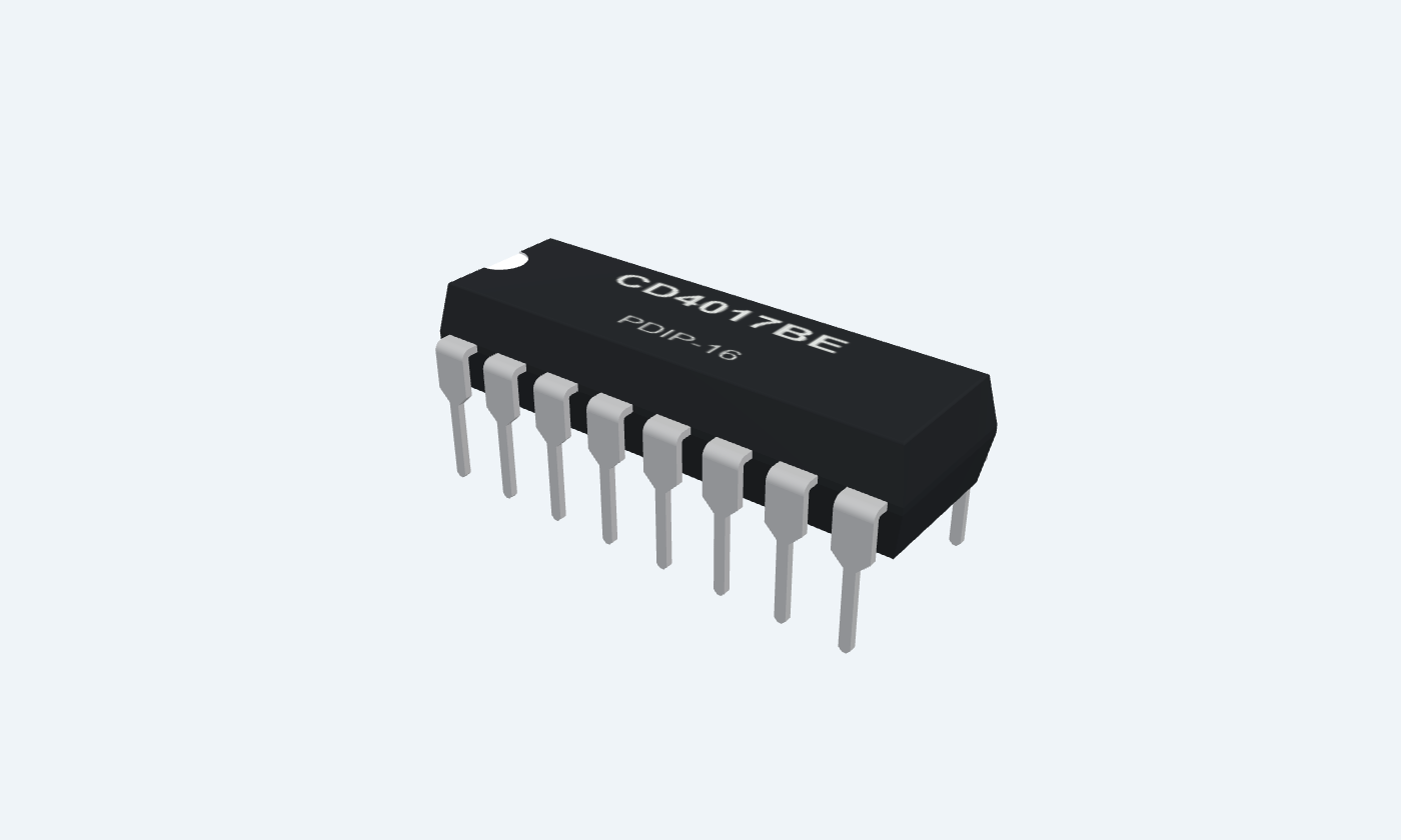
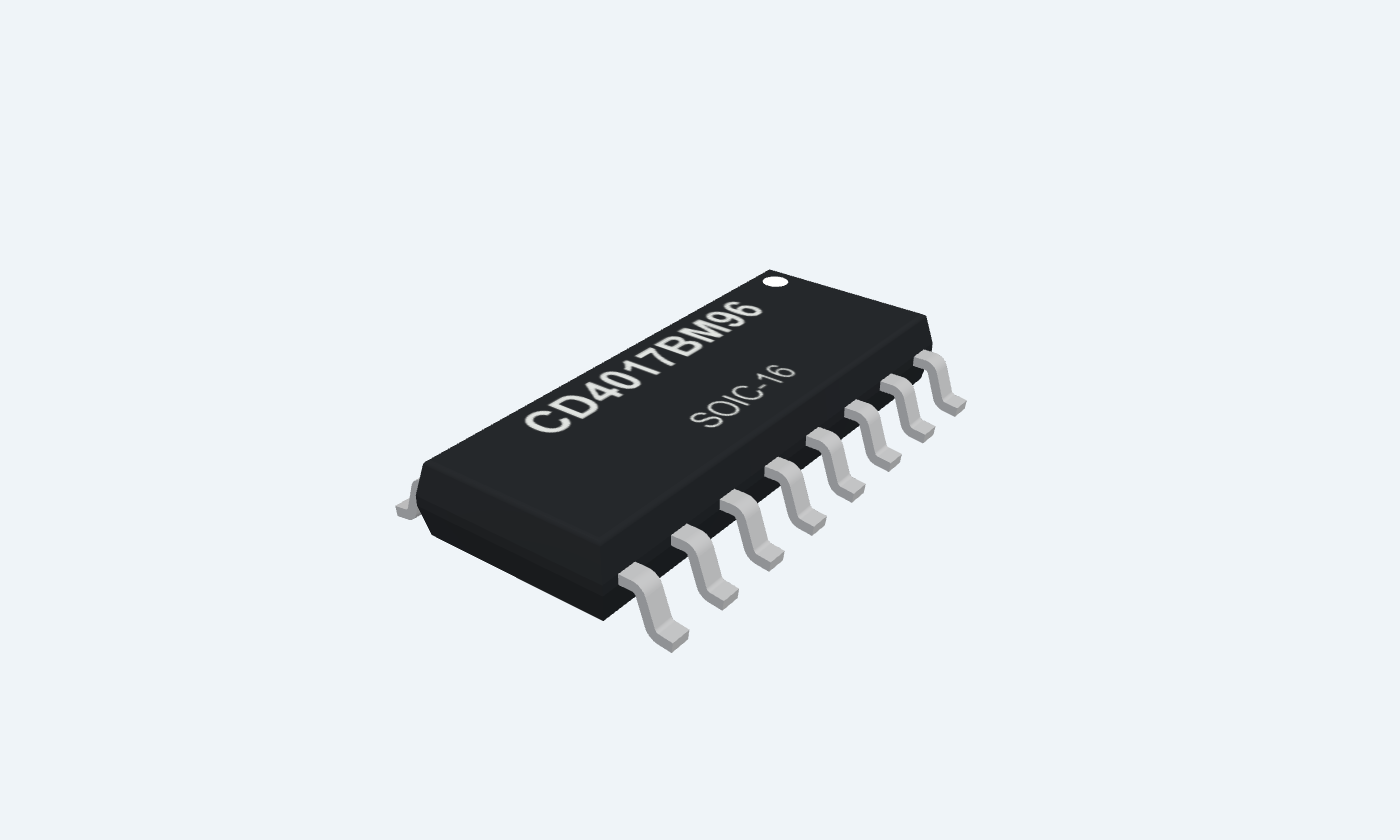
One clock. Ten steps. A visible sequence.
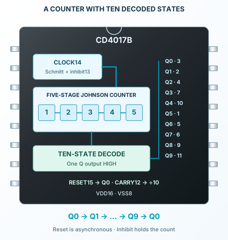
CD4017B is a decade counter with ten decoded outputs. Each accepted rising clock edge advances the HIGH output from Q0 through Q9, then returns to Q0. It uses a five-stage Johnson counter and decode logic inside one 16-pin IC. RESET is asynchronous and active HIGH. CLOCK INHIBIT holds the count when HIGH; the carry output is HIGH during counts 0–4 and LOW during counts 5–9. Reset the real device after power-up to establish a known starting state. This reference covers CD4017BE through-hole and CD4017BM96 surface-mount packages. The explorer starts from an applied reset and shows settled logic states; the circuit uses a clean 5 V clock and low-current LED indicators.
Click a lead or use the arrow keys. Top view
HIGH at count 5; LOW in the other nine states. Only one decoded output is HIGH at a time.
Leave open in the three-LED example.
Output drive is limited and depends on supply voltage and temperature.
HIGH at count 1; LOW in the other nine states. Only one decoded output is HIGH at a time.
Connect through 10 kΩ to a high-efficiency red LED, with its cathode to ground.
Output drive is limited and depends on supply voltage and temperature.
HIGH at count 0; LOW in the other nine states. Only one decoded output is HIGH at a time.
Connect through 10 kΩ to a high-efficiency red LED, with its cathode to ground.
Output drive is limited and depends on supply voltage and temperature.
HIGH at count 2; LOW in the other nine states. Only one decoded output is HIGH at a time.
Connect through 10 kΩ to a high-efficiency red LED, with its cathode to ground.
Output drive is limited and depends on supply voltage and temperature.
HIGH at count 6; LOW in the other nine states. Only one decoded output is HIGH at a time.
Leave open in the three-LED example.
Output drive is limited and depends on supply voltage and temperature.
HIGH at count 7; LOW in the other nine states. Only one decoded output is HIGH at a time.
Leave open in the three-LED example.
Output drive is limited and depends on supply voltage and temperature.
HIGH at count 3; LOW in the other nine states. Only one decoded output is HIGH at a time.
Leave open in the three-LED example.
Output drive is limited and depends on supply voltage and temperature.
Common return for the logic and output loads.
Connect to supply negative and the bypass return.
HIGH at count 8; LOW in the other nine states. Only one decoded output is HIGH at a time.
Leave open in the three-LED example.
Output drive is limited and depends on supply voltage and temperature.
HIGH at count 4; LOW in the other nine states. Only one decoded output is HIGH at a time.
Leave open in the three-LED example.
Output drive is limited and depends on supply voltage and temperature.
HIGH at count 9; LOW in the other nine states. Only one decoded output is HIGH at a time.
Leave open in the three-LED example.
Output drive is limited and depends on supply voltage and temperature.
HIGH for counts 0–4 and LOW for counts 5–9. It completes one cycle for every ten input pulses.
Leave open in the LED example; use a reviewed cascade connection for additional decades.
Carry is a five-count-wide state, not a narrow pulse at Q9.
HIGH prevents advancement from clock pin 14. LOW allows counting.
Connect to ground for continuous counting.
A HIGH-to-LOW transition here can count if clock14 is held HIGH; keep inhibit stable around clock edges.
A LOW-to-HIGH clock transition advances the count when inhibit is LOW and reset is LOW.
Use a clean 0–5 V, 1 Hz logic clock in the example.
Schmitt action permits slow clock edges; it does not remove mechanical switch bounce.
HIGH selects count zero immediately: Q0 HIGH, Q1–Q9 LOW and carry HIGH.
Use a momentary switch to +5 V and a 10 kΩ pull-down. Pulse it after power-up.
Hold LOW while counting. A deterministic starting state requires reset.
Supplies the counter, decoder and output buffers.
Use regulated +5 V and a local 100 nF capacitor to VSS8.
Recommended operating supply: 3–18 V.
Decade counter / divider
A clean clock advances the decoded HIGH output. Reset returns to Q0, while inhibit freezes the count. Carry supplies a divide-by-ten waveform.
CD4017BE
Key parameters and their test conditions
Follows the selected physical package
Select a pin to open its function, electrical notes and wiring guidance.
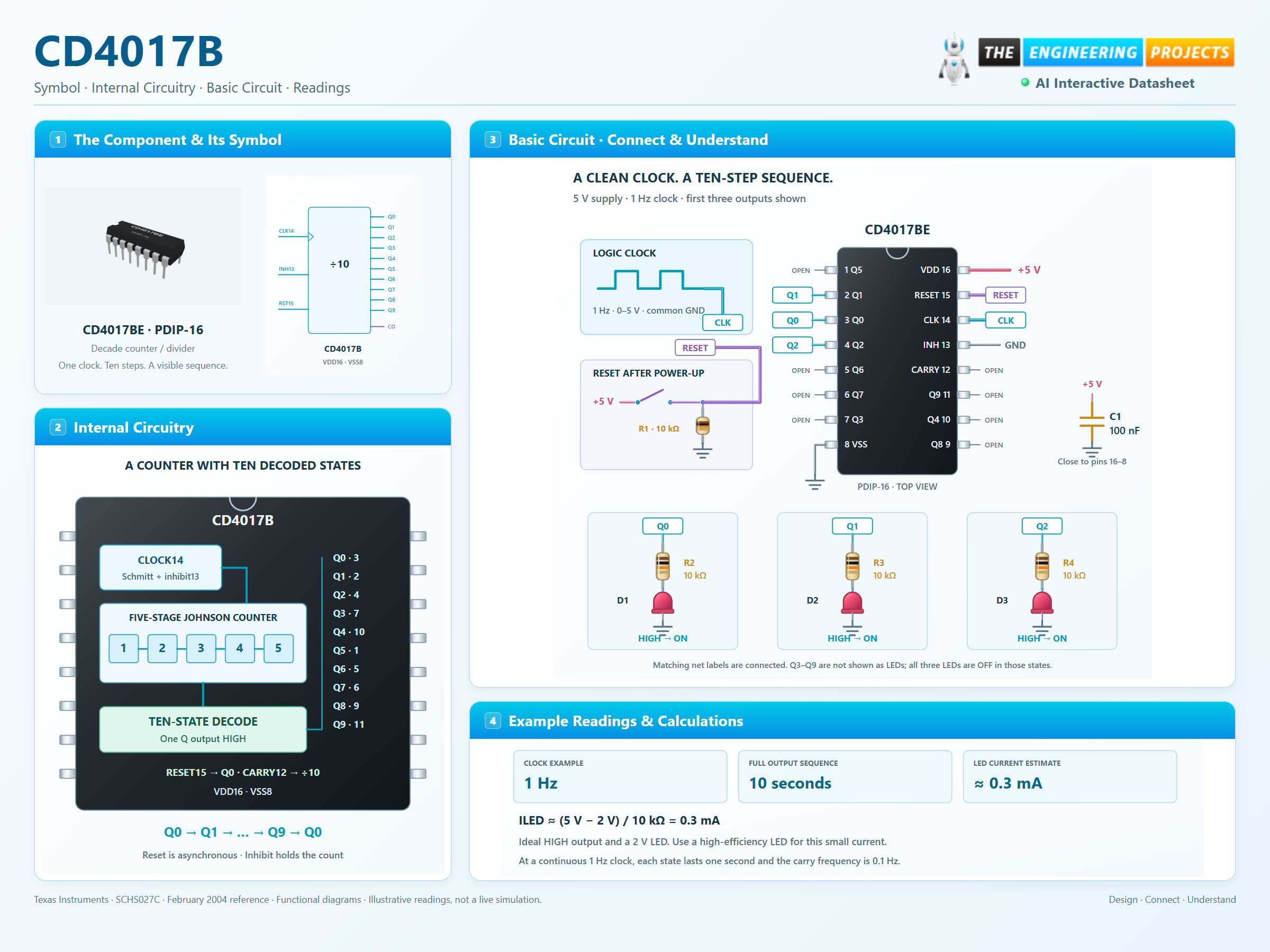
Pulse RESET HIGH after power-up, then return it LOW. Q0 becomes HIGH and carry is HIGH.
With INHIBIT LOW, each rising edge on CLOCK advances to the next output. Q9 wraps back to Q0.
Set INHIBIT HIGH to hold. Carry is HIGH for the first five states and LOW for the next five, providing divide-by-ten timing.
CD4017B stores a count, so the current output depends on previous clock edges. Reset establishes Q0, inhibit holds the state and carry divides the accepted clock by ten. It is not a binary-output counter.
Pulse the clock, hold the count or reset immediately to Q0.
Pulse sends LOW → HIGH → LOW. With inhibit HIGH, clock pulses hold the count. Reset HIGH immediately selects Q0 and keeps it selected.
Releasing inhibit while the clock is already HIGH also advances the hardware counter. Try it with the individual controls.
Starts after an applied reset. Shows settled logic only; propagation delay, switch bounce, analog thresholds and output loading are not simulated. Carry is HIGH for counts 0–4, LOW for counts 5–9.
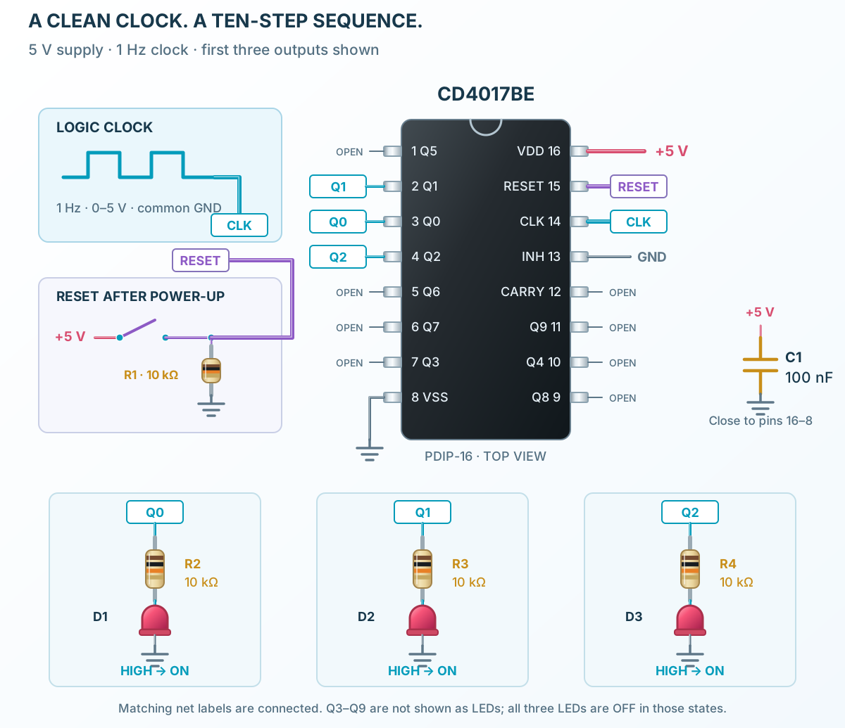
Select a pin to explore its function and connection.
| Pin | Signal | Type | Function |
|---|---|---|---|
| Q5 | Decoded push-pull output | HIGH at count 5; LOW in the other nine states. Only one decoded output is HIGH at a time. | |
| Q1 | Decoded push-pull output | HIGH at count 1; LOW in the other nine states. Only one decoded output is HIGH at a time. | |
| Q0 | Decoded push-pull output | HIGH at count 0; LOW in the other nine states. Only one decoded output is HIGH at a time. | |
| Q2 | Decoded push-pull output | HIGH at count 2; LOW in the other nine states. Only one decoded output is HIGH at a time. | |
| Q6 | Decoded push-pull output | HIGH at count 6; LOW in the other nine states. Only one decoded output is HIGH at a time. | |
| Q7 | Decoded push-pull output | HIGH at count 7; LOW in the other nine states. Only one decoded output is HIGH at a time. | |
| Q3 | Decoded push-pull output | HIGH at count 3; LOW in the other nine states. Only one decoded output is HIGH at a time. | |
| VSS | Ground return | Common return for the logic and output loads. | |
| Q8 | Decoded push-pull output | HIGH at count 8; LOW in the other nine states. Only one decoded output is HIGH at a time. | |
| Q4 | Decoded push-pull output | HIGH at count 4; LOW in the other nine states. Only one decoded output is HIGH at a time. | |
| Q9 | Decoded push-pull output | HIGH at count 9; LOW in the other nine states. Only one decoded output is HIGH at a time. | |
| CARRY | Divide-by-ten output | HIGH for counts 0–4 and LOW for counts 5–9. It completes one cycle for every ten input pulses. | |
| INHIBIT | Clock inhibit | HIGH prevents advancement from clock pin 14. LOW allows counting. | |
| CLOCK | Schmitt clock input | A LOW-to-HIGH clock transition advances the count when inhibit is LOW and reset is LOW. | |
| RESET | Asynchronous active-HIGH reset | HIGH selects count zero immediately: Q0 HIGH, Q1–Q9 LOW and carry HIGH. | |
| VDD | Positive supply | Supplies the counter, decoder and output buffers. |
No pins match. Try a signal name or choose All pins.
RESET establishes state zero
| Parameter | Value | Conditions / notes |
|---|---|---|
| Count 0 | Q0 HIGH · pin 3 | All other Q outputs LOW; carry HIGH |
| Count 1 | Q1 HIGH · pin 2 | All other Q outputs LOW; carry HIGH |
| Count 2 | Q2 HIGH · pin 4 | All other Q outputs LOW; carry HIGH |
| Count 3 | Q3 HIGH · pin 7 | All other Q outputs LOW; carry HIGH |
| Count 4 | Q4 HIGH · pin 10 | All other Q outputs LOW; carry HIGH |
| Count 5 | Q5 HIGH · pin 1 | All other Q outputs LOW; carry LOW |
| Count 6 | Q6 HIGH · pin 5 | All other Q outputs LOW; carry LOW |
| Count 7 | Q7 HIGH · pin 6 | All other Q outputs LOW; carry LOW |
| Count 8 | Q8 HIGH · pin 9 | All other Q outputs LOW; carry LOW |
| Count 9 | Q9 HIGH · pin 11 | All other Q outputs LOW; carry LOW |
No specifications match. Try a parameter name or a unit.
After Q9, the next accepted clock edge returns to Q0.
CD4017BE / CD4017BM96
| Parameter | Value | Conditions / notes |
|---|---|---|
| Operating supply | 3–18 V | 5 V in the example |
| Operating temperature | −55 to +125°C | Selected package grades |
| HIGH input at 5 V | At least 3.5 V | Manufacturer static test conditions |
| LOW input at 5 V | At most 1.5 V | Manufacturer static test conditions |
| Clock input | Rising-edge counting | INHIBIT LOW; RESET LOW |
| Reset input | HIGH selects Q0 | Asynchronous; no clock required |
| Clock inhibit | HIGH holds the count | Falling inhibit can count if CLOCK is HIGH |
| Clock14 rise / fall time | No specified limit | Schmitt action on CLOCK14; not a debounce function |
No specifications match. Try a parameter name or a unit.
The alternate clock use of pin13 has different transition requirements; see the manufacturer footnote.
5 V supply unless stated
| Parameter | Value | Conditions / notes |
|---|---|---|
| Source at VOH = 4.6 V | 0.51 mA minimum at 25°C | 0.36 mA minimum at 125°C; manufacturer test |
| Sink at VOL = 0.4 V | 0.51 mA minimum at 25°C | 0.36 mA minimum at 125°C; manufacturer test |
| No-load output HIGH | At least 4.95 V | 5 V supply |
| No-load output LOW | At most 0.05 V | 5 V supply |
| Quiescent current | 0.04 µA typical; 5 µA maximum | 25°C, 5 V, inputs at supply rails |
| Quiescent current over temperature | 150 µA maximum at 5 V | 85°C and 125°C entries |
| Input capacitance | 5 pF typical | Any input |
No specifications match. Try a parameter name or a unit.
Do not read output current from the absolute stress limits. LED loads lower the HIGH level and increase current consumption.
25°C · CL = 50 pF · RL = 200 kΩ
| Parameter | Value | Conditions / notes |
|---|---|---|
| Clock-to-decoded output | 325 ns typical; 650 ns maximum | 5 V; input transitions 20 ns |
| Clock-to-carry output | 300 ns typical; 600 ns maximum | 5 V; input transitions 20 ns |
| Clock frequency capability | 2.5 MHz minimum; 5 MHz typical | 5 V; measured with carry output |
| Minimum clock pulse width | 200 ns | 5 V recommended condition |
| Inhibit setup time | 230 ns | 5 V before the clock edge |
| Reset pulse width | 260 ns minimum | 5 V recommended condition |
| Reset removal time | 400 ns minimum | 5 V recommended condition |
No specifications match. Try a parameter name or a unit.
Typical speed is not a guarantee for every supply, load and temperature. The manual explorer does not reproduce these delays.
A clean 1 Hz, 0–5 V clock
| Parameter | Value | Conditions / notes |
|---|---|---|
| Clock input | Pin 14 | Common-ground logic clock |
| Clock inhibit | Pin 13 → GND | Allows counting |
| Reset network | Pin 15 → 10 kΩ → GND | Momentary switch to +5 V; pulse at startup |
| LED channels | Q0 pin 3, Q1 pin 2, Q2 pin 4 | One 10 kΩ series resistor per LED |
| LED current estimate | About 0.3 mA per active LED | Ideal 5 V HIGH and 2 V red LED |
| Supply bypass | 100 nF between pins 16 and 8 | Place close to the IC |
| Unused outputs and carry | Leave open | Counts 3–9 have no lit LED in this example |
No specifications match. Try a parameter name or a unit.
Use high-efficiency LEDs for this small drive current, or external drivers for bright/multiple loads. A manual clock switch requires debouncing.
Stress limits, not operating settings
| Parameter | Value | Conditions / notes |
|---|---|---|
| Supply voltage | −0.5 to +20 V | Recommended operation is 3–18 V |
| Input voltage | −0.5 V to VDD + 0.5 V | Referenced to VSS |
| Input current | ±10 mA | Any one input |
| Package dissipation | 500 mW through 100°C | Derate 12 mW/°C to 200 mW at 125°C |
| Output-transistor dissipation | 100 mW | Per output transistor |
| Storage temperature | −65 to +150°C | Unpowered storage |
No specifications match. Try a parameter name or a unit.
Supply and thermal stress ratings do not establish a safe output load.
Light successive indicators with a clean clock and suitable current limiting.
Manufacturer application guideUse the carry waveform to obtain one cycle for ten accepted clock pulses.
Manufacturer application guideUse the decoded states as logic selections; buffer loads that exceed the available output drive.
Manufacturer application guideFind CD4017B in the Components Library to place its schematic symbol and connect its pins.
Reference page · circuit simulation model not yet availableOpen ProTech