Real View
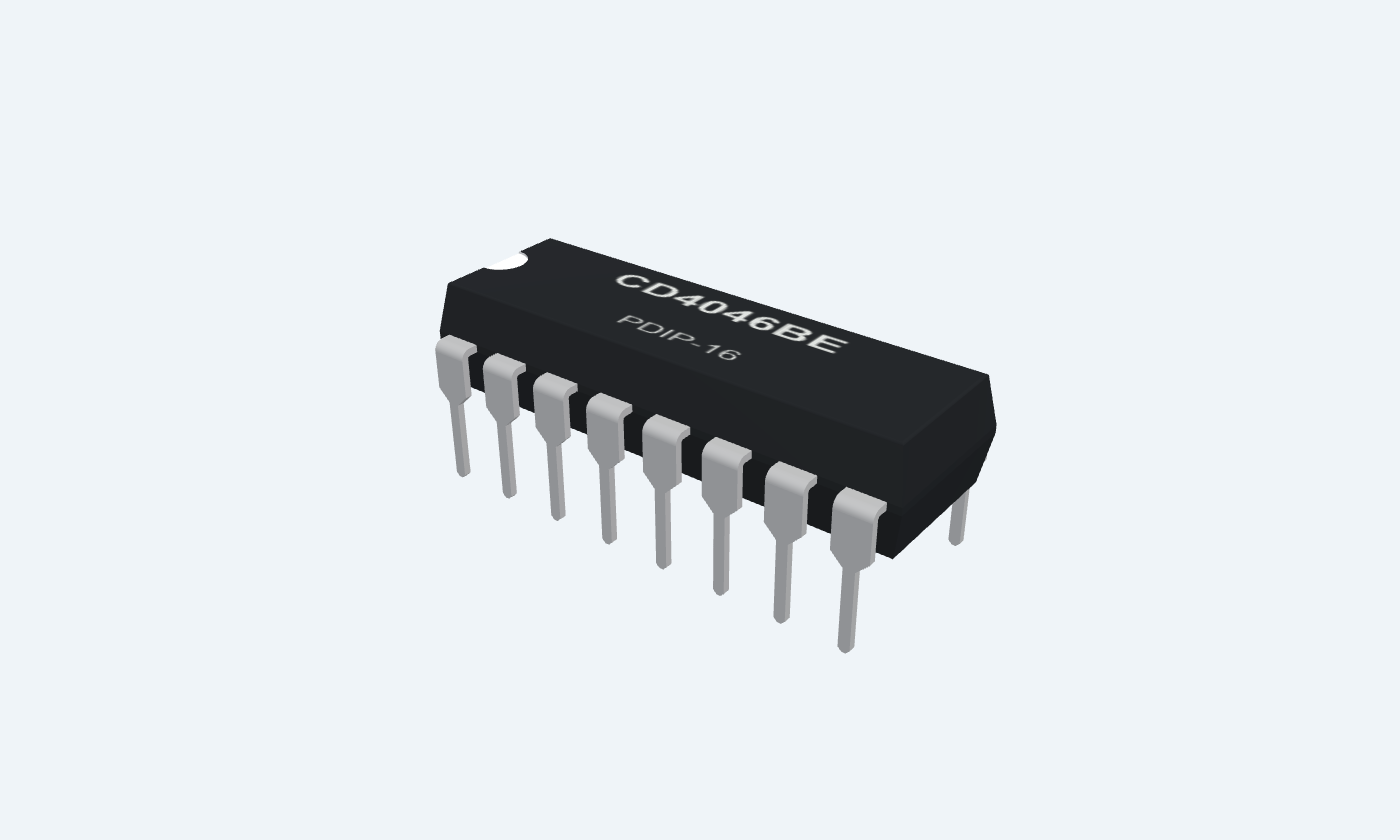
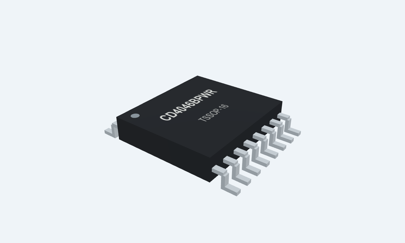
Compare phase. Control frequency. Build a feedback loop.
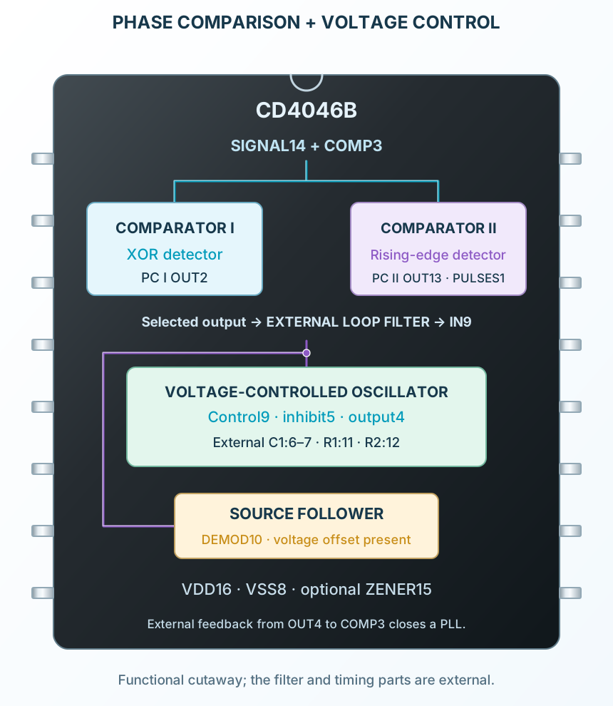
CD4046B combines a voltage-controlled oscillator and two different phase comparators in a 16-pin CMOS IC. External resistors and a capacitor establish the oscillator range; an analog control voltage changes its frequency. With feedback and an external low-pass filter, the oscillator can follow an incoming signal. Comparator I uses XOR logic, while comparator II compares rising edges and can leave its output in high impedance. Their capture behavior and phase relationships are different. Start with the illustrated 5 V oscillator: a potentiometer controls pin 9, a 10 nF capacitor joins pins 6 and 7, and 100 kΩ sets R1. The package switch compares CD4046BE PDIP-16 and CD4046BPWR TSSOP-16 with matching physical pin numbers.
Click a lead or use the arrow keys. Top view
Phase-pulse output associated with comparator II; HIGH when the two rising edges coincide in lock.
Leave open in the standalone VCO circuit.
This is not a universal lock detector; interpret its pulses in the complete loop.
Logic XOR of the conditioned signal and comparator inputs. Its average depends on phase and duty cycle.
Leave open in the VCO circuit; use an appropriate external low-pass filter for PLL operation.
Receives VCO output directly or through a divider in a PLL.
Ground in the standalone VCO example.
Do not tie it to an output while also grounding it.
CMOS square-wave output from the voltage-controlled oscillator.
Connect to a high-impedance oscilloscope or counter.
Use a buffer for substantial loads; this is not a power output.
LOW enables the oscillator. HIGH stops the VCO and associated source follower.
Tie to GND for continuous oscillation.
First terminal of the external VCO timing capacitor.
Connect a 10 nF non-polar capacitor between pins 6 and 7.
The capacitor goes between these pins, not from either pin to ground.
Second terminal of the external VCO timing capacitor.
Connect to the other end of the 10 nF timing capacitor.
Lower supply rail and common signal reference.
Connect to supply return, scope ground, potentiometer return and bypass capacitor.
High-impedance analog input that controls VCO frequency.
Connect to the wiper of a 10 kΩ potentiometer across 5 V and GND.
Keep inside the supply rails; avoid floating wiper connections.
Source-follower output related to VCO IN, with a substantial voltage offset.
Leave open when unused; when used connect at least 10 kΩ load resistance to VSS.
It is not an exact unity-gain or rail-to-rail copy of pin 9.
External R1 with C1 establishes the VCO frequency range.
Connect 100 kΩ from pin 11 to GND.
Optional R2 to VSS adds a minimum-frequency offset.
Leave open in the no-offset example.
Open means no R2; do not replace it with a short to ground.
Sources, sinks or enters high impedance according to the relative rising edges of the two inputs.
Leave open in the VCO circuit; connect through a designed loop filter in a PLL.
Common signal input for both phase comparators, with a self-biasing input stage for suitable AC coupling.
Ground in the standalone VCO circuit.
A DC-coupled 5 V signal must meet the stated CMOS input thresholds.
Contact for the internal zener diode, intended for a properly current-limited supply arrangement.
Leave open with the regulated 5 V supply in this example.
Do not connect directly across an unrestricted supply.
Supplies the oscillator and phase-comparator sections.
Use regulated 5 V; place 100 nF directly between pins 16 and 8.
CMOS phase-locked loop with VCO
The VCO works independently, or becomes part of a PLL with the chosen comparator and an external loop filter.
CD4046BE
Key parameters and their test conditions
Follows the selected physical package
Select a pin to open its function, electrical notes and wiring guidance.
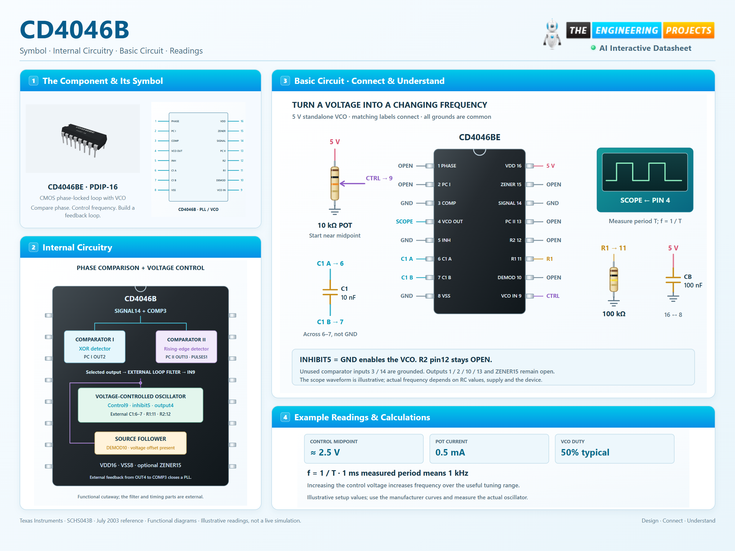
C1 connects between pins 6 and 7. R1 connects pin 11 to VSS; an optional R2 at pin 12 sets the lower-frequency offset.
With INHIBIT LOW, changing VCO IN changes the square-wave frequency. Observe pin 4 with a high-impedance scope.
Feed pin 4 back to COMP IN, apply the reference to SIGNAL IN, and return the selected comparator output through a designed low-pass filter to VCO IN.
The example demonstrates VCO control, not a closed PLL. A useful PLL also needs a reviewed loop filter, input levels and tuning range.
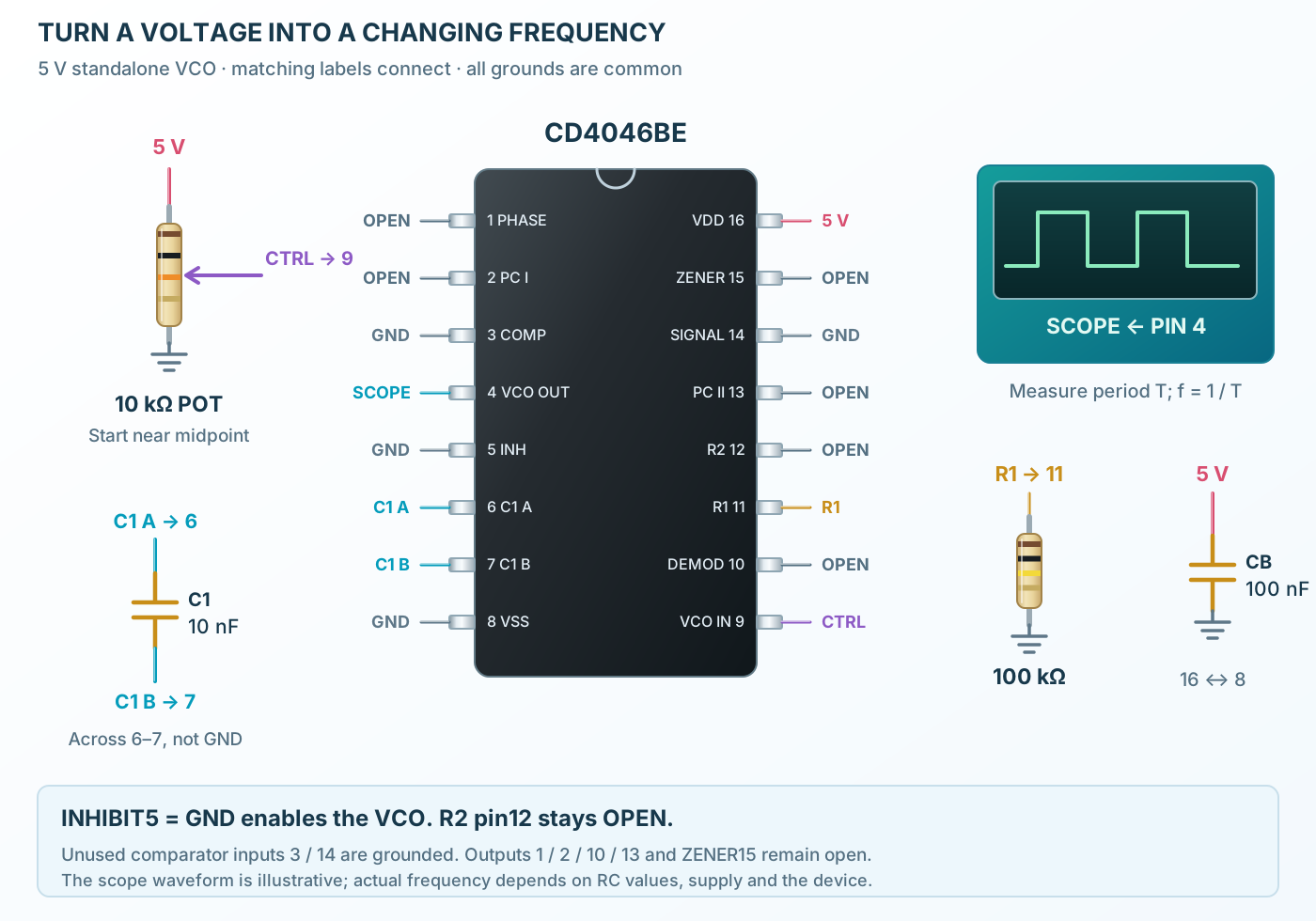
Select a pin to explore its function and connection.
| Pin | Signal | Type | Function |
|---|---|---|---|
| PHASE PULSES | Phase-comparator-II indicator | Phase-pulse output associated with comparator II; HIGH when the two rising edges coincide in lock. | |
| PC I OUT | Exclusive-OR comparator output | Logic XOR of the conditioned signal and comparator inputs. Its average depends on phase and duty cycle. | |
| COMP IN | Feedback comparator input | Receives VCO output directly or through a divider in a PLL. | |
| VCO OUT | Oscillator output | CMOS square-wave output from the voltage-controlled oscillator. | |
| INHIBIT | Active-HIGH VCO inhibit | LOW enables the oscillator. HIGH stops the VCO and associated source follower. | |
| C1 A | Timing capacitor contact | First terminal of the external VCO timing capacitor. | |
| C1 B | Timing capacitor contact | Second terminal of the external VCO timing capacitor. | |
| VSS | Ground reference | Lower supply rail and common signal reference. | |
| VCO IN | Oscillator control voltage | High-impedance analog input that controls VCO frequency. | |
| DEMOD OUT | Buffered control voltage | Source-follower output related to VCO IN, with a substantial voltage offset. | |
| R1 | Frequency-range resistor | External R1 with C1 establishes the VCO frequency range. | |
| R2 | Frequency-offset resistor | Optional R2 to VSS adds a minimum-frequency offset. | |
| PC II OUT | Edge-controlled comparator output | Sources, sinks or enters high impedance according to the relative rising edges of the two inputs. | |
| SIGNAL IN | Reference signal input | Common signal input for both phase comparators, with a self-biasing input stage for suitable AC coupling. | |
| ZENER | Optional shunt reference | Contact for the internal zener diode, intended for a properly current-limited supply arrangement. | |
| VDD | Positive supply | Supplies the oscillator and phase-comparator sections. |
No pins match. Try a signal name or choose All pins.
Use the correct supply for the intended mode
| Parameter | Value | Conditions / notes |
|---|---|---|
| PLL operation | 5–18 V | Recommended range |
| Standalone fixed oscillator / comparators | 3–18 V | Separate manufacturer operating entries |
| Ambient temperature | −55 to +125°C | Selected PDIP and TSSOP orderables |
| 5 V logic LOW / HIGH | ≤1.5 V / ≥3.5 V | DC-coupled comparator inputs |
| Timing resistors | 5 kΩ to 1 MΩ | Manufacturer design guidance |
| Timing capacitor at ≥5 V | At least 100 pF | At ≥10 V guidance permits 50 pF |
No specifications match. Try a parameter name or a unit.
Nominal operating conditions are distinct from absolute maximum stress limits.
The two outputs are not interchangeable
| Parameter | Value | Conditions / notes |
|---|---|---|
| Comparator I | XOR output at pin 2 | Duty-cycle dependent; use 50% input duty for maximum lock range |
| Comparator I at center frequency | About 90° phase difference | Nominal locked condition |
| Comparator II | Edge-controlled output at pin 13 | Uses positive transitions; source / sink / high-Z |
| Comparator II in lock | Nominal zero phase difference | Ideal aligned edges; filter retains control voltage |
| Harmonic lock | Possible with comparator I | Comparator II avoids the stated harmonic-center lock behavior |
| No reference input | I tends toward center; II toward minimum | As described for the respective complete loops |
No specifications match. Try a parameter name or a unit.
Actual acquisition, ripple and stability depend on the external filter and signal conditions.
Complete sixteen-pin device
| Parameter | Value | Conditions / notes |
|---|---|---|
| Power | VDD16 / VSS8 | Local 100 nF bypass |
| VCO | OUT4 / IN9 / INHIBIT5 | Control and oscillator output |
| Timing | C1 across 6–7; R1 at11; R2 at12 | Resistors return to VSS |
| Reference / feedback | SIGNAL IN14 / COMP IN3 | Shared by both comparators |
| Comparator outputs | PC I2 / PC II13 / phase pulses1 | Select the correct feedback path |
| Auxiliary | DEMOD10 / ZENER15 | Leave open when unused |
No specifications match. Try a parameter name or a unit.
Package switching retains these signal assignments.
Typical performance requires its stated setup
| Parameter | Value | Conditions / notes |
|---|---|---|
| Output duty cycle | 50% typical | Specified at 5, 10 and 15 V |
| Typical maximum frequency | 1.4 MHz | 10 V, R1 5 kΩ, C1 50 pF, R2 open, VCO IN=VDD |
| Power example | 70 µW typical | 5 V, 10 kHz, R1 1 MΩ, R2 open, VCO IN=VDD/2 |
| Range adjustment | R1 and C1 | Use manufacturer curves; calibrate the built circuit |
| Frequency offset | R2 to VSS | Omit R2 for the no-offset configuration |
| Inhibit | LOW enables; HIGH disables | Also switches off the associated source follower |
No specifications match. Try a parameter name or a unit.
The 1.4 MHz point is not a guaranteed frequency for the 5 V example.
A clear starting circuit, not a closed PLL
| Parameter | Value | Conditions / notes |
|---|---|---|
| Supply | 5 V; 100 nF bypass | VDD16 to VSS8 |
| Control | 10 kΩ potentiometer across rails | Wiper to VCO IN9; start near 2.5 V |
| Timing capacitor | 10 nF non-polar | Between pins 6 and 7 |
| Range resistor | 100 kΩ | Pin 11 to GND |
| Offset resistor | Not fitted | Pin 12 remains open |
| Enable | Pin 5 to GND | VCO runs |
| Unused comparator inputs | Pins 3 and 14 to GND | Defined inputs |
| Unused outputs / reference | Pins 1, 2, 10, 13 and 15 open | Do not ground output pins |
| Measurement | Pin 4 to high-impedance scope | Scope ground to VSS |
No specifications match. Try a parameter name or a unit.
Sweep slowly, observe the measured frequency and avoid loading timing nodes.
Illustrative setup values
| Parameter | Value | Conditions / notes |
|---|---|---|
| Potentiometer midpoint | About 2.5 V | 5 V supply; unloaded ideal midpoint |
| Potentiometer current | 5 V / 10 kΩ = 0.5 mA | External control network only |
| Increasing control voltage | Frequency increases over the useful tuning range | Endpoint behavior and exact slope are device-dependent |
| Period measurement | f = 1 / T | Measure consecutive equivalent edges on pin 4 |
| Example measured period | 1 ms means 1 kHz | Unit conversion only, not a prediction for the shown RC |
| PLL lock | Not applicable to this standalone circuit | No comparator feedback filter is connected |
No specifications match. Try a parameter name or a unit.
Calculated setup quantities are not live simulation results.
CD4046BE · PDIP-16
| Parameter | Value | Conditions / notes |
|---|---|---|
| PDIP | CD4046BE · 16 pins | 2.54 mm lead pitch |
| TSSOP | CD4046BPWR · 16 pins | 0.65 mm pitch; TI PW0016A |
| SOP alternative | CD4046BNSR | Different body and land pattern; not the selected TSSOP |
| Supply stress limit | 20 V absolute maximum | Recommended operation remains at or below 18 V |
| Input voltage stress | VSS−0.5 to VDD+0.5 V | Not a valid operating signal range |
| Input current stress | ±10 mA absolute maximum | Do not design for continuous clamp injection |
| Storage temperature | −65 to +150°C | Unpowered |
No specifications match. Try a parameter name or a unit.
Use the selected package drawing and review fabrication tolerances before making a PCB.
Use a designed PLL to track a compatible periodic signal.
Manufacturer application guideAdd a feedback divider and a properly compensated loop.
Manufacturer application guideExplore modulation and demodulation with specified deviation and filtering.
Manufacturer application guideFind CD4046B in the Components Library to place its schematic symbol and connect its pins.
Reference page · circuit simulation model not yet availableOpen ProTech