CD4051BEight-channel bidirectional analog multiplexer
Route one of eight analog signals to a shared connection.
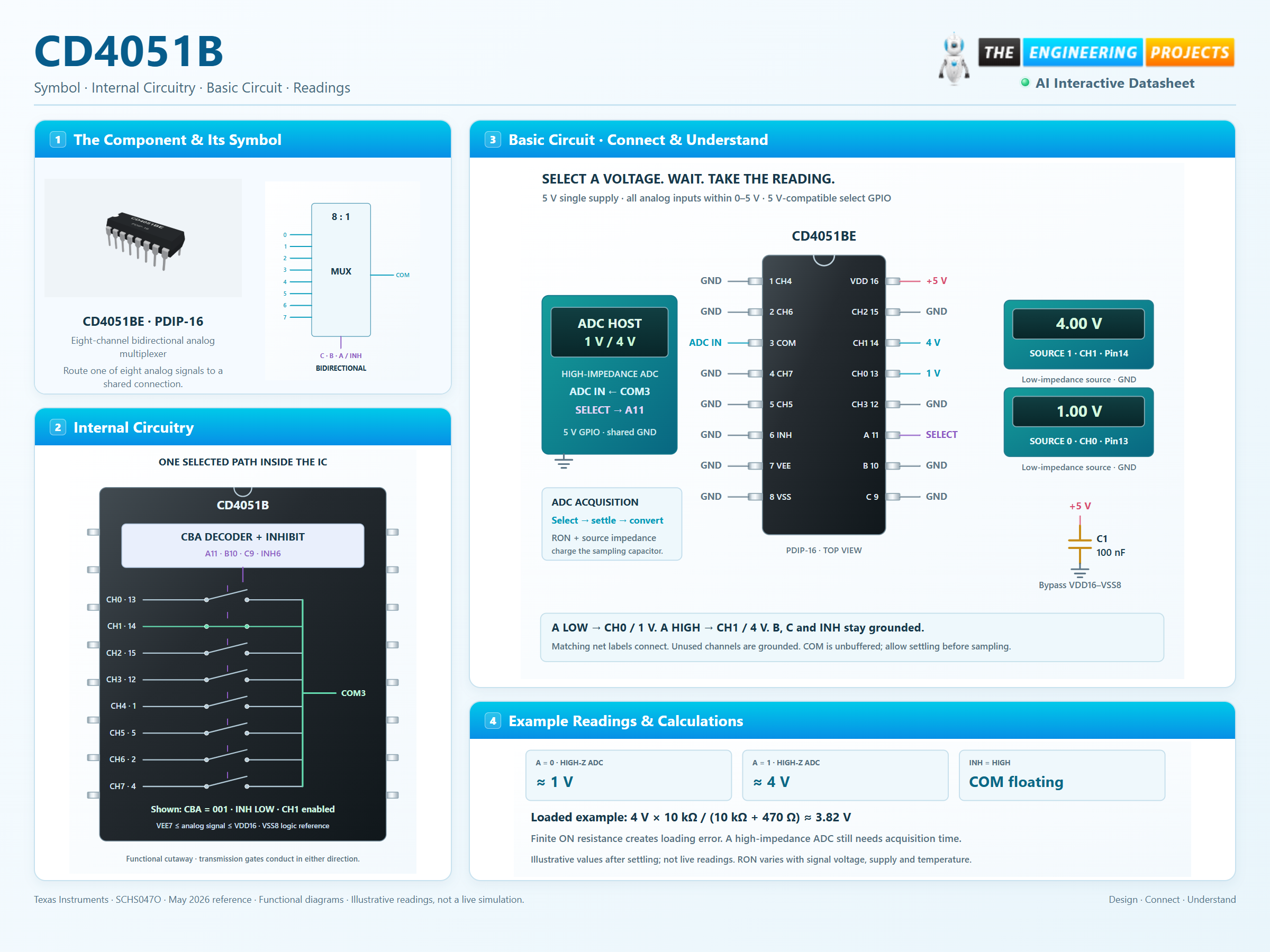
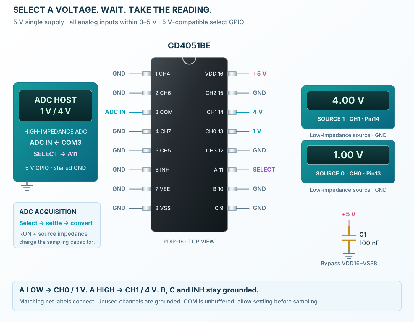
CD4051B connects one of eight analog channels to a common terminal. Three digital inputs select the channel, and a separate inhibit input opens all paths. Signals can travel in either direction through the selected switch; the IC does not amplify or regenerate them. The analog range is set by VEE and VDD, while select and inhibit controls are referenced to VSS and VDD. In the 5 V single-supply circuit, VEE and VSS are both grounded, so all analog signals stay between 0 V and 5 V. Negative signals require a suitable negative VEE rail and a compatible complete circuit. The example routes either a 1 V or 4 V low-impedance source into a high-impedance ADC. Switch resistance, source impedance and sampling capacitance determine settling and error. Firmware selects the channel, waits for acquisition to settle and only then records a conversion.

Bidirectional signal pathsSelect & inhibitAnalog rails & logic ground
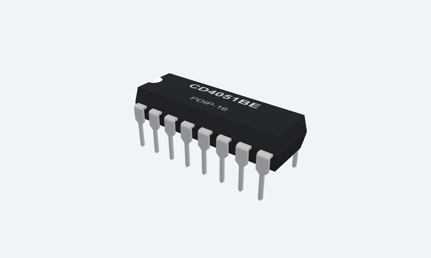
CD4051BEPDIP-16Top view
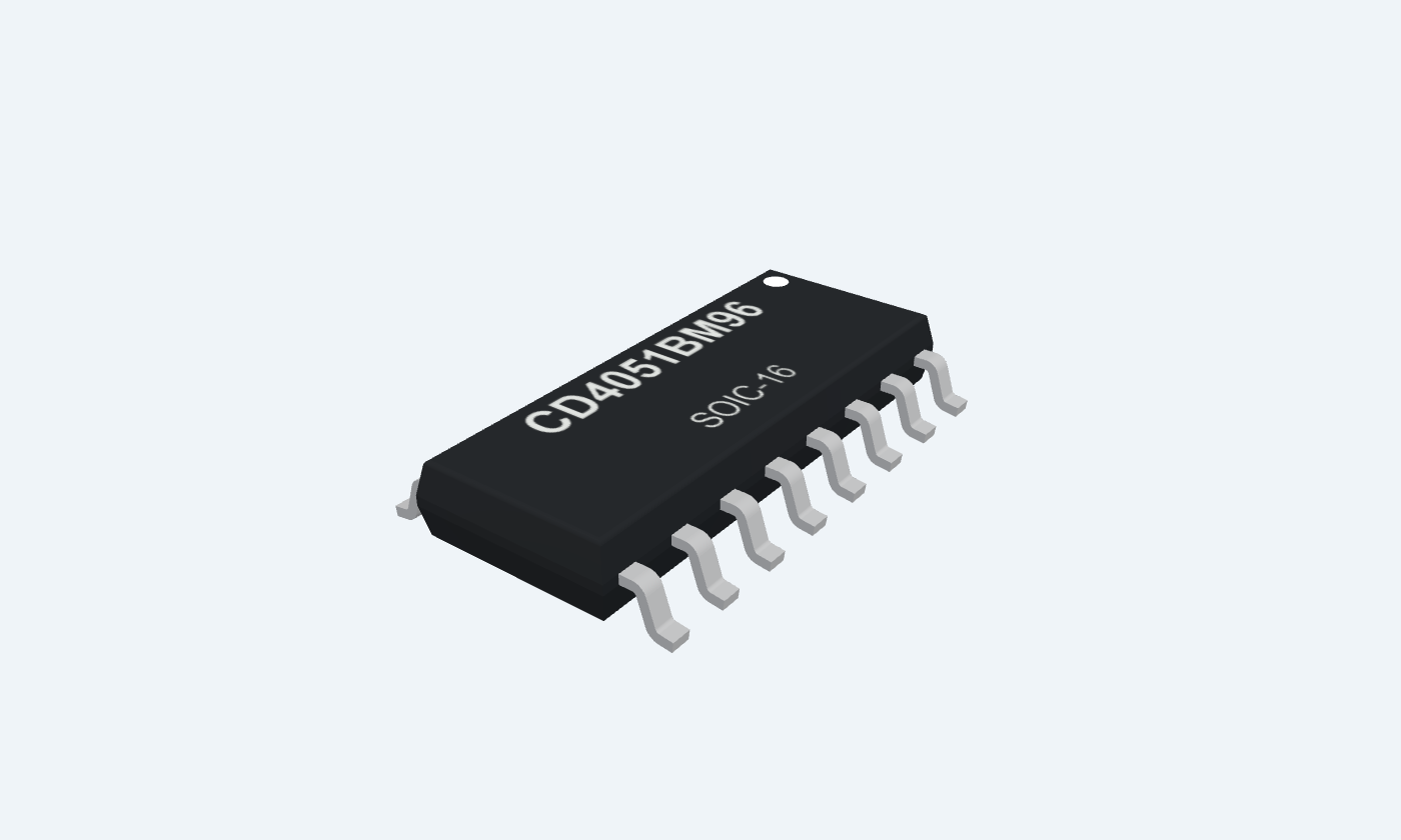
CD4051BM96SOIC-16Top view
Click a lead or use the arrow keys. Top view
PIN 1 · Bidirectional signal paths
Bidirectional analogCH4
Function
Channel 4 connects to COM when INH is LOW and CBA selects 4.
How to connect
Tie unused channels to GND in this example.
Electrical note
Keep the signal within VEE–VDD. The enabled channel has finite, signal-dependent resistance.
PIN 2 · Bidirectional signal paths
Bidirectional analogCH6
Function
Channel 6 connects to COM when INH is LOW and CBA selects 6.
How to connect
Tie unused channels to GND in this example.
Electrical note
Keep the signal within VEE–VDD. The enabled channel has finite, signal-dependent resistance.
PIN 3 · Bidirectional signal paths
Bidirectional commonCOM
Function
Shared terminal of the selected analog channel; may be used as input or output.
How to connect
Connect to a high-impedance 5 V-compatible ADC input.
Electrical note
Not a buffered amplifier output. Allow settling before sampling.
PIN 4 · Bidirectional signal paths
Bidirectional analogCH7
Function
Channel 7 connects to COM when INH is LOW and CBA selects 7.
How to connect
Tie unused channels to GND in this example.
Electrical note
Keep the signal within VEE–VDD. The enabled channel has finite, signal-dependent resistance.
PIN 5 · Bidirectional signal paths
Bidirectional analogCH5
Function
Channel 5 connects to COM when INH is LOW and CBA selects 5.
How to connect
Tie unused channels to GND in this example.
Electrical note
Keep the signal within VEE–VDD. The enabled channel has finite, signal-dependent resistance.
PIN 6 · Select & inhibit
Active-HIGH inhibitINH
Function
HIGH opens every signal path, regardless of address.
How to connect
Ground for continuous selection; a controller may drive HIGH while changing address.
Electrical note
When disabled, COM may float; the ADC can retain an old charge.
PIN 7 · Analog rails & logic ground
Analog lower railVEE
Function
Lowest allowed analog signal level.
How to connect
Connect to GND for the single-supply example.
Electrical note
A negative rail is possible in a reviewed dual-supply design; VSS remains the logic reference.
PIN 8 · Analog rails & logic ground
Logic groundVSS
Function
Digital control reference and supply return.
How to connect
Connect to controller ground.
PIN 9 · Select & inhibit
Digital select inputC
Function
Binary channel-selection weight 4; A is the least significant bit.
How to connect
Ground in the two-source example.
Electrical note
Use valid control levels relative to VSS and VDD; never leave floating.
PIN 10 · Select & inhibit
Digital select inputB
Function
Binary channel-selection weight 2; A is the least significant bit.
How to connect
Ground in the two-source example.
Electrical note
Use valid control levels relative to VSS and VDD; never leave floating.
PIN 11 · Select & inhibit
Digital select inputA
Function
Binary channel-selection weight 1; A is the least significant bit.
How to connect
Drive with a 0/5 V GPIO to select CH0 or CH1.
Electrical note
Use valid control levels relative to VSS and VDD; never leave floating.
PIN 12 · Bidirectional signal paths
Bidirectional analogCH3
Function
Channel 3 connects to COM when INH is LOW and CBA selects 3.
How to connect
Tie unused channels to GND in this example.
Electrical note
Keep the signal within VEE–VDD. The enabled channel has finite, signal-dependent resistance.
PIN 13 · Bidirectional signal paths
Bidirectional analogCH0
Function
Channel 0 connects to COM when INH is LOW and CBA selects 0.
How to connect
Connect the 1 V low-impedance source in the example.
Electrical note
Keep the signal within VEE–VDD. The enabled channel has finite, signal-dependent resistance.
PIN 14 · Bidirectional signal paths
Bidirectional analogCH1
Function
Channel 1 connects to COM when INH is LOW and CBA selects 1.
How to connect
Connect the 4 V low-impedance source in the example.
Electrical note
Keep the signal within VEE–VDD. The enabled channel has finite, signal-dependent resistance.
PIN 15 · Bidirectional signal paths
Bidirectional analogCH2
Function
Channel 2 connects to COM when INH is LOW and CBA selects 2.
How to connect
Tie unused channels to GND in this example.
Electrical note
Keep the signal within VEE–VDD. The enabled channel has finite, signal-dependent resistance.
PIN 16 · Analog rails & logic ground
Positive supplyVDD
Function
Upper analog rail and positive logic supply.
How to connect
Use +5 V and 100 nF to VSS8 close to the IC.
At a glance
Eight-channel bidirectional analog multiplexer
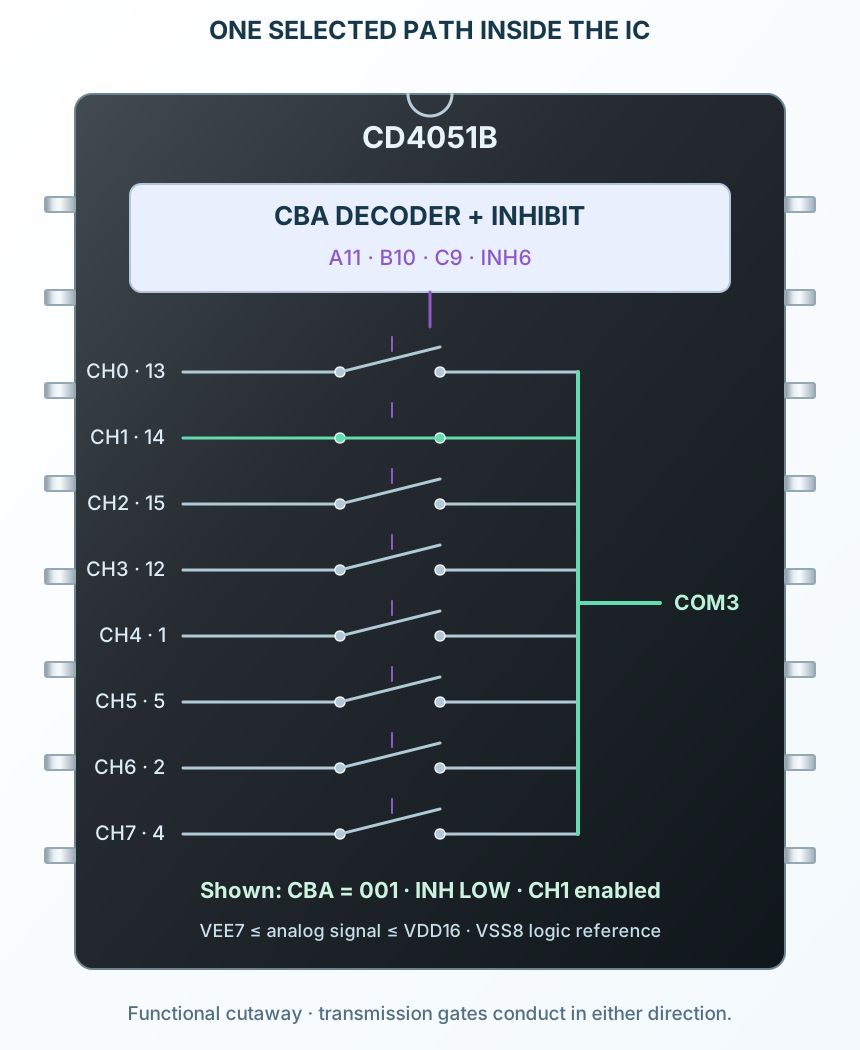
A decoder controls eight transmission gates. One channel reaches COM when enabled; a HIGH inhibit signal disconnects all eight.
8 One common terminalSignal channels
5 V · VEE and VSS groundedExample supply
−55–125 °CSelected variants
470 Ω at 5 V / 25°CTypical ON resistance
Operating profile
CD4051BE
Channel-selection map
Key parameters and their test conditions
- CBA = 000
- CH0 · pin 13Conditions / notes: Connected bidirectionally to COM pin 3
- CBA = 001
- CH1 · pin 14Conditions / notes: Connected bidirectionally to COM pin 3
- CBA = 010
- CH2 · pin 15Conditions / notes: Connected bidirectionally to COM pin 3
- CBA = 011
- CH3 · pin 12Conditions / notes: Connected bidirectionally to COM pin 3
- CBA = 100
- CH4 · pin 1Conditions / notes: Connected bidirectionally to COM pin 3
- CBA = 101
- CH5 · pin 5Conditions / notes: Connected bidirectionally to COM pin 3
Package details
Follows the selected physical package
- Manufacturer
- Texas Instruments
- Part number
- CD4051BE
- Package
- PDIP-16
- Connections
- 16 pins
- Mounting
- Through-hole
- Lead pitch
- 2.54 mm
- Package code
- dip
- Thermal reference
- Board and package dependent; see manufacturer data
Connections by function
Select a pin to open its function, electrical notes and wiring guidance.
Bidirectional signal paths9 pins
Select & inhibit4 pins
Analog rails & logic ground3 pins
Bidirectional signal paths9 pins
Select & inhibit4 pins
Analog rails & logic ground3 pins
Keep signals inside the rails
Use VEE and VDD as the analog boundaries; all example signals remain within 0–5 V.
Select the channel
Hold INH LOW and present CBA. A is weight 1, B weight 2 and C weight 4.
Wait and sample
Allow the selected source to settle at the ADC before taking a reading. A disabled common pin is not a defined zero.
An analog multiplexer is a switch, not an ADC or an amplifier. Check rail limits and control thresholds, then budget acquisition time for the switch and source resistance.
Pin reference
Select a pin to explore its function and connection.
16 pins
| Pin | Signal | Type | Function |
|---|---|---|---|
| CH4 | Bidirectional analog | Channel 4 connects to COM when INH is LOW and CBA selects 4. | |
| CH6 | Bidirectional analog | Channel 6 connects to COM when INH is LOW and CBA selects 6. | |
| COM | Bidirectional common | Shared terminal of the selected analog channel; may be used as input or output. | |
| CH7 | Bidirectional analog | Channel 7 connects to COM when INH is LOW and CBA selects 7. | |
| CH5 | Bidirectional analog | Channel 5 connects to COM when INH is LOW and CBA selects 5. | |
| INH | Active-HIGH inhibit | HIGH opens every signal path, regardless of address. | |
| VEE | Analog lower rail | Lowest allowed analog signal level. | |
| VSS | Logic ground | Digital control reference and supply return. | |
| C | Digital select input | Binary channel-selection weight 4; A is the least significant bit. | |
| B | Digital select input | Binary channel-selection weight 2; A is the least significant bit. | |
| A | Digital select input | Binary channel-selection weight 1; A is the least significant bit. | |
| CH3 | Bidirectional analog | Channel 3 connects to COM when INH is LOW and CBA selects 3. | |
| CH0 | Bidirectional analog | Channel 0 connects to COM when INH is LOW and CBA selects 0. | |
| CH1 | Bidirectional analog | Channel 1 connects to COM when INH is LOW and CBA selects 1. | |
| CH2 | Bidirectional analog | Channel 2 connects to COM when INH is LOW and CBA selects 2. | |
| VDD | Positive supply | Upper analog rail and positive logic supply. |
No pins match. Try a signal name or choose All pins.
Channel-selection map
INH LOW enables selection
Manufacturer specifications 8 parameters
| Parameter | Value | Conditions / notes |
|---|---|---|
| CBA = 000 | CH0 · pin 13 | Connected bidirectionally to COM pin 3 |
| CBA = 001 | CH1 · pin 14 | Connected bidirectionally to COM pin 3 |
| CBA = 010 | CH2 · pin 15 | Connected bidirectionally to COM pin 3 |
| CBA = 011 | CH3 · pin 12 | Connected bidirectionally to COM pin 3 |
| CBA = 100 | CH4 · pin 1 | Connected bidirectionally to COM pin 3 |
| CBA = 101 | CH5 · pin 5 | Connected bidirectionally to COM pin 3 |
| CBA = 110 | CH6 · pin 2 | Connected bidirectionally to COM pin 3 |
| CBA = 111 | CH7 · pin 4 | Connected bidirectionally to COM pin 3 |
No specifications match. Try a parameter name or a unit.
INH HIGH opens all paths, independent of CBA.
Rails and control levels
5 V single-supply example
Manufacturer specifications 6 parameters
| Parameter | Value | Conditions / notes |
|---|---|---|
| VDD / VSS / VEE | +5 V / 0 V / 0 V | Pins 16 / 8 / 7 |
| Analog terminal range | VEE to VDD | 0–5 V in this example |
| Control HIGH | 3.5 V minimum at VDD 5 V | Select and inhibit inputs |
| Control LOW | 0.8 V maximum | Current SCHS047O specification |
| 3.3 V controller at 5 V supply | HIGH is not guaranteed | Use suitable level translation |
| Negative analog signals | Require an appropriate negative VEE | Do not apply below ground with VEE grounded |
No specifications match. Try a parameter name or a unit.
Digital and analog voltage domains are related but have different lower references.
Switch resistance
TA 25°C; VEE = VSS = 0 V
Manufacturer specifications 6 parameters
| Parameter | Value | Conditions / notes |
|---|---|---|
| At VDD 5 V | 470 Ω typical; 1050 Ω maximum | Across the specified signal range |
| At VDD 10 V | 180 Ω typical; 400 Ω maximum | Specified test conditions |
| At VDD 15 V | 125 Ω typical; 240 Ω maximum | Specified test conditions |
| At 5 V / +125°C | 1300 Ω maximum | Temperature changes resistance |
| Channel-to-channel difference | 15 Ω typical at 5 V | Not the absolute channel resistance |
| Load interaction | Creates a divider with the load | Keep source and load conditions explicit |
No specifications match. Try a parameter name or a unit.
The typical 125 Ω headline belongs to 15 V operation; it is not a 5 V value.
Propagation and acquisition
Timing is not the same as ADC settling
Manufacturer specifications 6 parameters
| Parameter | Value | Conditions / notes |
|---|---|---|
| Signal path at 5 V | 30 ns typical; 60 ns maximum | RL 200 kΩ, CL 50 pF, TA 25°C |
| Address-to-output at 5 V | 450 ns typical; 720 ns maximum | RL 10 kΩ, CL 50 pF, 20 ns edges |
| Inhibit-to-ON at 5 V | 400 ns typical; 720 ns maximum | RL 1 kΩ, CL 50 pF, 20 ns edges |
| Inhibit-to-OFF at 5 V | 200 ns typical; 450 ns maximum | RL 10 kΩ, CL 50 pF, 20 ns edges |
| ADC acquisition | Depends on source, switch and sampling capacitor | Use the ADC manufacturer timing requirements |
| Simple RC estimate | τ = (Rsource + RON) × C | Only a first-order model |
No specifications match. Try a parameter name or a unit.
Propagation specifications do not promise a precision ADC result immediately after selection.
Two-source ADC wiring
Same 5 V logic and analog domain
Manufacturer specifications 7 parameters
| Parameter | Value | Conditions / notes |
|---|---|---|
| Power | VDD16 +5 V; VSS8 and VEE7 GND | 100 nF local bypass |
| CH0 pin13 | 1 V low-impedance source | Select with A LOW |
| CH1 pin14 | 4 V low-impedance source | Select with A HIGH |
| COM pin3 | High-impedance ADC input | Wait for acquisition settling |
| Select | B10 and C9 grounded | A11 driven by a 0/5 V GPIO |
| Enable | INH6 grounded | Optional GPIO can inhibit between readings |
| Unused channels | Pins 15, 12, 1, 5, 2 and 4 grounded | No unused digital input is left floating |
No specifications match. Try a parameter name or a unit.
Named source labels refer to the same nets throughout the illustration.
Expected readings and loading
Illustrative calculation; not live measurement
Manufacturer specifications 6 parameters
| Parameter | Value | Conditions / notes |
|---|---|---|
| A = 0, B = C = 0 | Approximately 1 V at COM | High-impedance load after settling |
| A = 1, B = C = 0 | Approximately 4 V at COM | High-impedance load after settling |
| INH = 1 | No defined COM voltage | Leakage and stored charge remain |
| 4 V into a 10 kΩ load | 4 × 10000 / (10000 + 470) = 3.82 V | Assumes zero source resistance and 470 Ω RON |
| Loading error in that estimate | About −4.49% | Actual RON changes with voltage and temperature |
| High-impedance sampling | Reduces static loading | Acquisition capacitance still needs charging time |
No specifications match. Try a parameter name or a unit.
Do not confuse the ideal selected-source value with a guaranteed loaded output voltage.
Package and practical limits
CD4051BE · PDIP-16
Manufacturer specifications 6 parameters
| Parameter | Value | Conditions / notes |
|---|---|---|
| Through-hole | CD4051BE · PDIP-16 | 2.54 mm pin pitch |
| Surface-mount | CD4051BM96 · SOIC-16 | 1.27 mm pitch; 3.9 mm body |
| Operating temperature | −55 to +125°C | Selected orderables |
| Storage temperature | −65 to +150°C | Unpowered |
| Rail sequencing | Prevent signals driving an unpowered device | Consider source current and clamp paths |
| Unused control inputs | Tie to a valid logic level | Do not rely on floating CMOS inputs |
No specifications match. Try a parameter name or a unit.
This reference follows the current TI revision and a conservative 5 V example; consult the full datasheet for other supply arrangements.
Shared ADC input
Select several bounded, compatible sensor voltages for a single converter input.
Manufacturer application guideAnalog routing
Switch low-current analog paths while accounting for resistance and capacitance.
Manufacturer application guideSignal distribution
Drive COM and select one channel when a bidirectional demultiplexer is useful.
Manufacturer application guideTake it into ProTech
Find CD4051B in the Components Library to place its schematic symbol and connect its pins.
Reference page · circuit simulation model not yet availableOpen ProTech