Real View
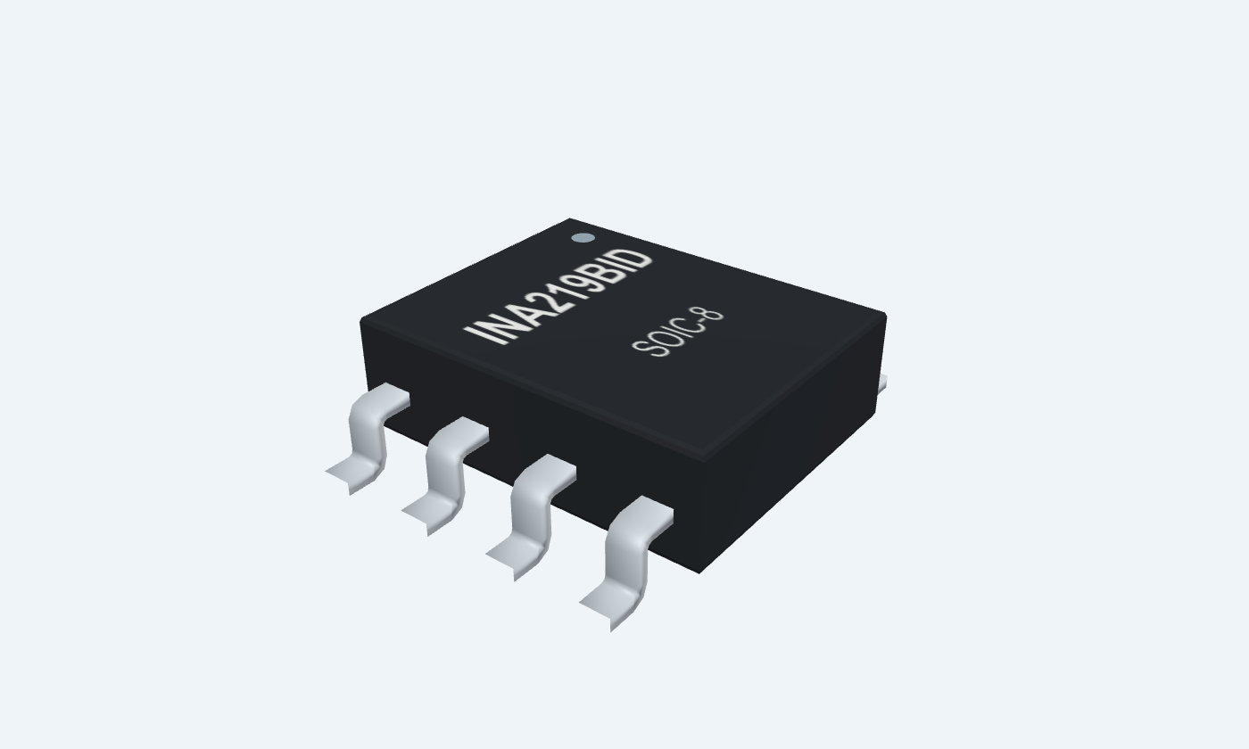
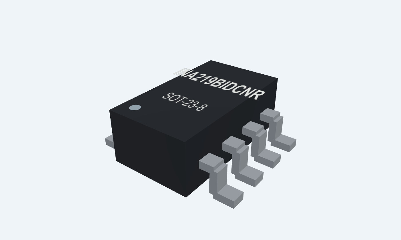
Measure the shunt drop, bus voltage and load power.
INA219 measures current by sensing the small voltage across an external shunt resistor. It also measures the load-side bus voltage relative to ground, then provides digital voltage, current and power registers over I²C. Its logic supply is separate from the measured bus, allowing a 3.3 V controller to monitor a bus up to 26 V. The shunt value and programmed calibration determine the current scale. Raw voltage measurements work without this calibration, but the current and power registers need a valid calibration value. This page uses the B accuracy grade and distinguishes its SOIC-8 pin numbers from those of the smaller SOT-23-8 package. The example places a 0.1 Ω Kelvin-sensed shunt ahead of a 12 Ω load on a 12 V source. Nominal current is about 0.992 A and the load receives about 11.90 V. A 0.1 mA current LSB gives calibration 4096; those readings are illustrative calculations, not measurements from a connected circuit.
Click a lead or use the arrow keys. Top view
Upper address-selection input.
Tie to ground for 0x40 with A0 also low.
SOIC pin 1; SOT-23 pin 8.
Lower address-selection input.
Tie to ground in the example.
SOIC pin 2; SOT-23 pin 7. Both address inputs can select GND, VS, SDA or SCL.
Open-drain I²C data.
Connect host SDA and a 4.7 kΩ pull-up to 3.3 V.
SOIC pin 3; SOT-23 pin 6.
Clock from the host.
Connect host SCL with pull-up to 3.3 V.
SOIC pin 4; SOT-23 pin 5.
Powers the measurement electronics.
Use 3.3 V and 100 nF locally.
3–5.5 V supply. SOIC pin 5; SOT-23 pin 4.
Reference for bus voltage and logic.
Join measured-system ground and controller ground.
SOIC pin 6; SOT-23 pin 3. This is not an isolated monitor.
Load-side shunt connection; bus voltage is measured here relative to GND.
Kelvin sense to the load side of the 0.1 Ω shunt.
SOIC pin 7; SOT-23 pin 2.
Source-side shunt connection. Positive current produces IN+ above IN−.
Kelvin sense to the supply side of the shunt.
SOIC pin 8; SOT-23 pin 1. Recommended measured bus range 0–26 V.
I²C bidirectional current and power monitor
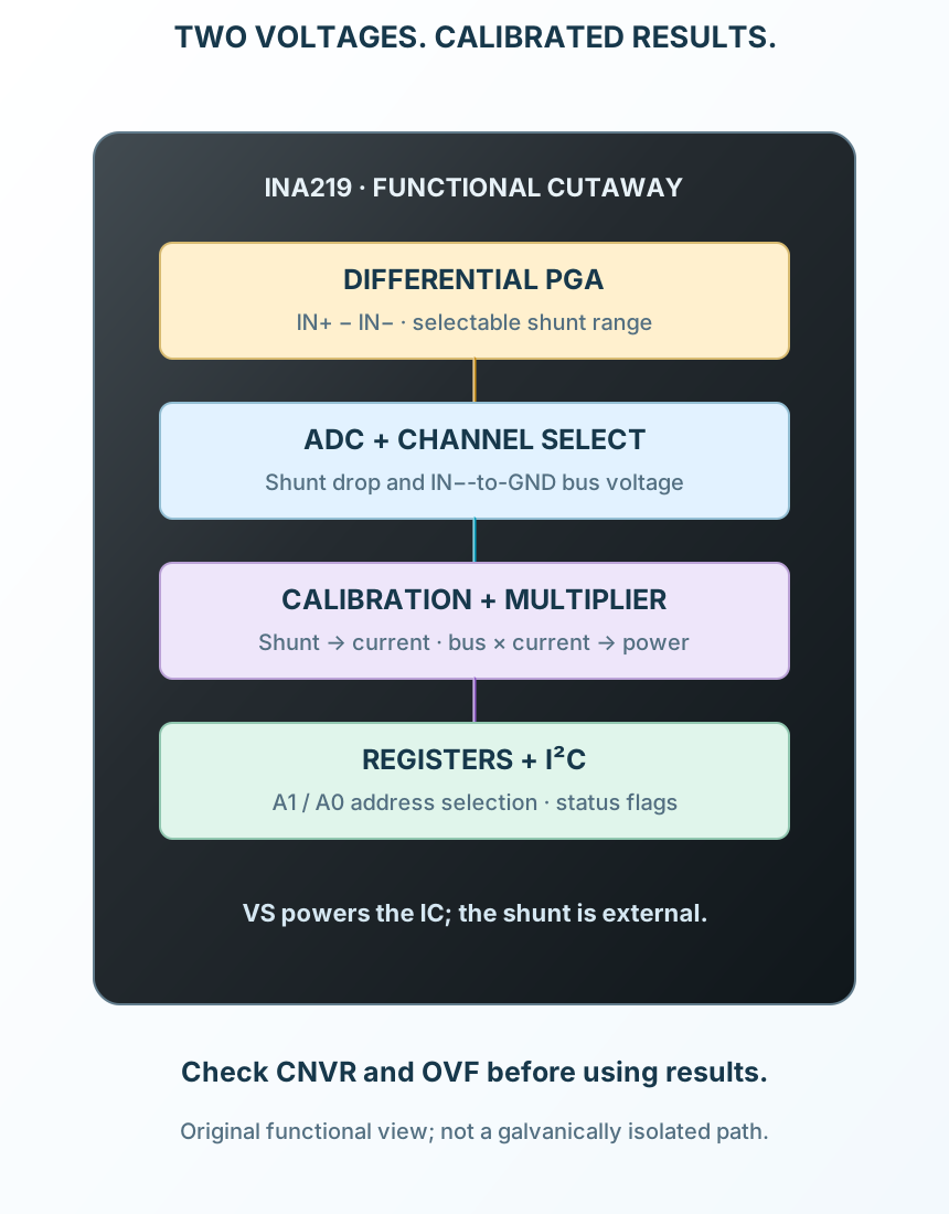
A programmable front end measures the shunt. A second conversion measures the bus. Calibration scales current, and a multiplier produces power.
INA219BID
Key parameters and their test conditions
Follows the selected physical package
Select a pin to open its function, electrical notes and wiring guidance.
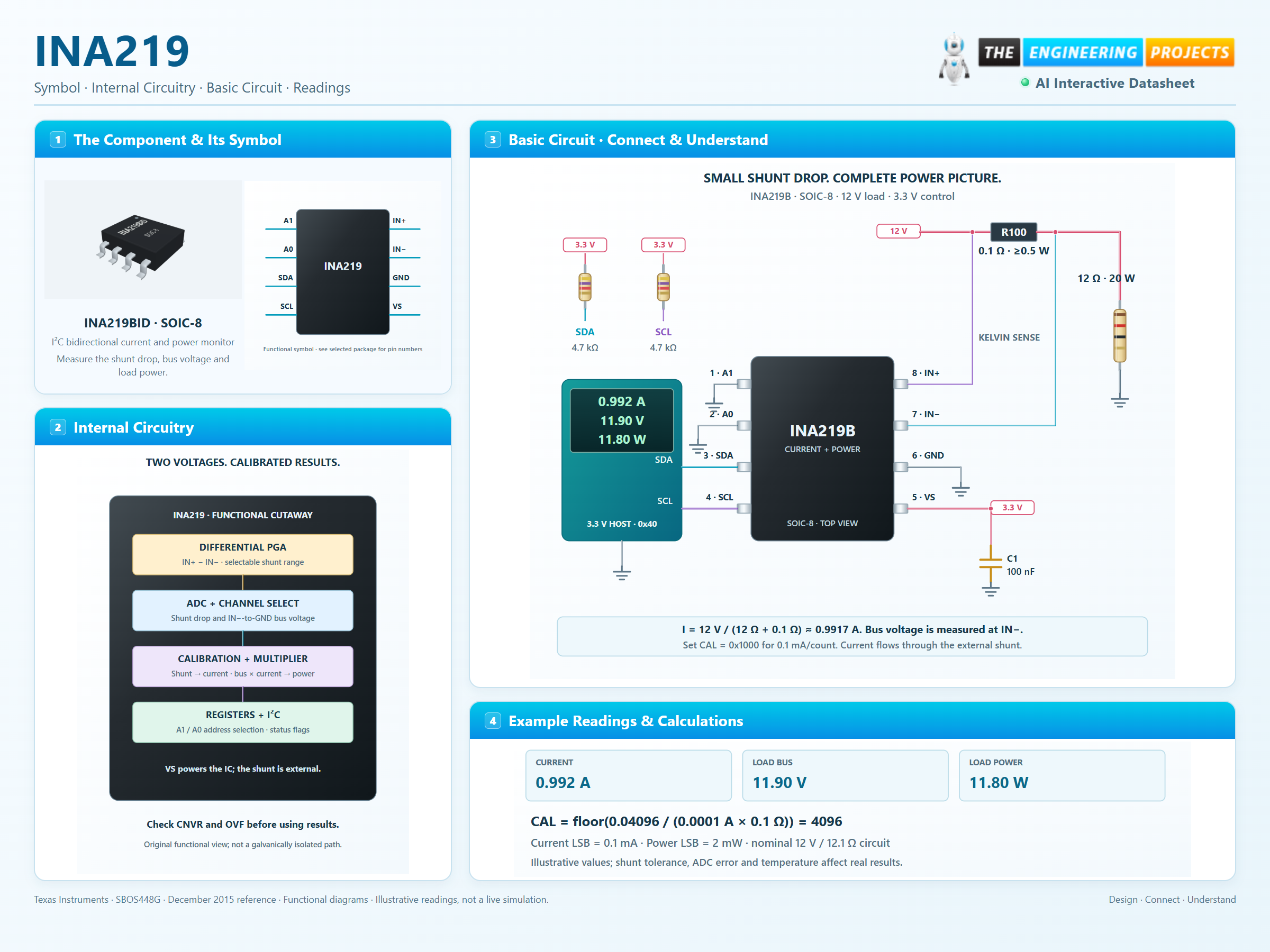
Route a separate pair of Kelvin traces from the resistor pads to IN+ and IN−.
Choose a current LSB and write the corresponding integer to the calibration register.
Check conversion-ready and overflow status, then apply the correct voltage/current/power scales.
Current_LSB = 0.1 mA and RSHUNT = 0.1 Ω give CAL = floor(0.04096 / (0.0001 × 0.1)) = 4096. Power_LSB = 20 × Current_LSB = 2 mW.
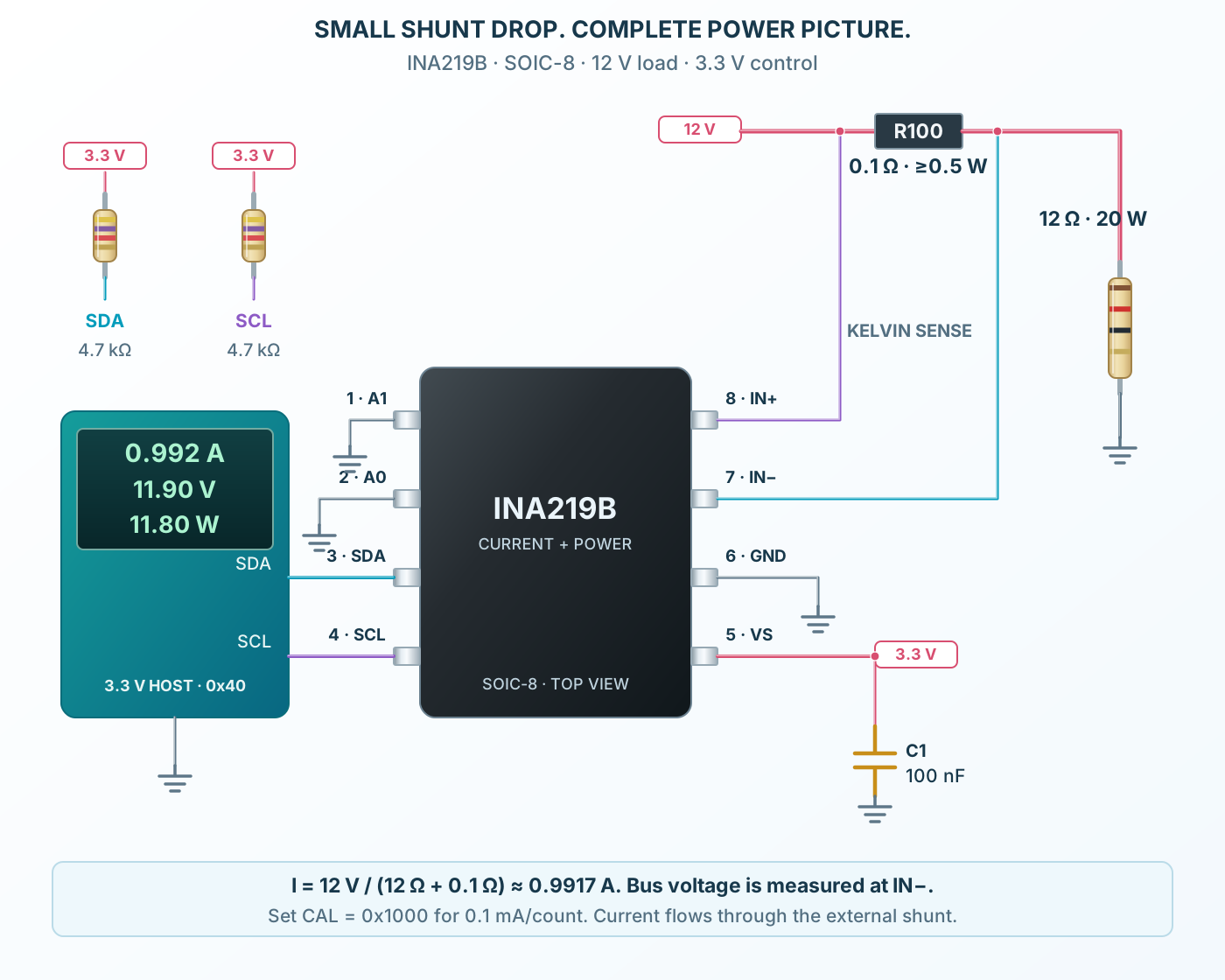
Select a pin to explore its function and connection.
| Pin | Signal | Type | Function |
|---|---|---|---|
| A1 | Address input | Upper address-selection input. | |
| A0 | Address input | Lower address-selection input. | |
| SDA | Serial data | Open-drain I²C data. | |
| SCL | Serial clock | Clock from the host. | |
| VS | Device supply | Powers the measurement electronics. | |
| GND | Ground | Reference for bus voltage and logic. | |
| IN− | Shunt negative input | Load-side shunt connection; bus voltage is measured here relative to GND. | |
| IN+ | Shunt positive input | Source-side shunt connection. Positive current produces IN+ above IN−. |
No pins match. Try a signal name or choose All pins.
B grade selected; conditions matter
| Parameter | Value | Conditions / notes |
|---|---|---|
| Device supply VS | 3–5.5 V | Independent of the monitored bus |
| Measured bus | 0–26 V | Do not confuse the 32 V register range with allowed pin voltage |
| Shunt full scale | ±40, ±80, ±160 or ±320 mV | PGA selection |
| Shunt resolution | 10 µV per LSB | Signed voltage register |
| Bus resolution | 4 mV per LSB | Shift register right by 3 before scaling |
| Quiescent current | 700 µA typical; 1 mA maximum | Specified operating conditions |
| Operating temperature | −40 to +125°C | Selected industrial device |
No specifications match. Try a parameter name or a unit.
A negative differential shunt reading is allowed; the individual sense terminals still obey their common-mode limits.
Six 16-bit registers
| Parameter | Value | Conditions / notes |
|---|---|---|
| 0x00 Configuration | Range, PGA, ADC and mode | Reset default 0x399F |
| 0x01 Shunt voltage | Signed raw × 10 µV | Negative current gives a negative result |
| 0x02 Bus voltage | (raw >> 3) × 4 mV | Bit 1 CNVR, bit 0 OVF |
| 0x03 Power | Unsigned raw × Power_LSB | Power_LSB = 20 × Current_LSB |
| 0x04 Current | Signed raw × Current_LSB | Requires calibration |
| 0x05 Calibration | Integer calibration value | Reset value zero disables current/power calculation |
No specifications match. Try a parameter name or a unit.
Read register data MSB first. Do not treat the status bits in the bus register as voltage bits.
0.1 Ω example
| Parameter | Value | Conditions / notes |
|---|---|---|
| Chosen current LSB | 0.0001 A | 0.1 mA per count |
| Calibration formula | floor(0.04096 / (Current_LSB × RSHUNT)) | Use amperes and ohms |
| Example calibration | 4096 = 0x1000 | Program register 0x05 |
| Power LSB | 0.002 W | 20 times current LSB |
| Current register positive ceiling | 3.2767 A | 32767 counts at the chosen scale |
| Shunt full-scale current | 3.2 A at ±320 mV | 0.320 / 0.1; this is lower than the register ceiling |
| Shunt heating at 1 A | 0.1 W | Choose power rating, tolerance and temperature coefficient deliberately |
No specifications match. Try a parameter name or a unit.
A different shunt requires recalibration. Arithmetic overflow makes current and power readings invalid.
Single-channel time, before combining bus and shunt
| Parameter | Value | Conditions / notes |
|---|---|---|
| 9-bit conversion | 84 µs | One selected voltage channel |
| 10 / 11 / 12 bit | 148 / 276 / 532 µs | Single conversion |
| 128-sample averaging | 68.10 ms | One channel; two channels take longer |
| Continuous shunt + bus | Two sequential conversions | Default 12-bit settings give about 1.064 ms total |
| Triggered mode | One selected measurement sequence | Poll CNVR |
| I²C | Standard, fast and high-speed modes | Up to 2.56 MHz with the defined high-speed protocol |
| Power-down | Conversions stopped | Digital interface remains accessible |
No specifications match. Try a parameter name or a unit.
Averaging reduces update speed; it does not increase the bus clock or guarantee more absolute accuracy.
A1/A0 may connect to four defined sources
| Parameter | Value | Conditions / notes |
|---|---|---|
| A1 GND, A0 GND | 0x40 | Example address |
| A1 GND, A0 VS | 0x41 | Seven-bit address |
| A1 GND, A0 SDA | 0x42 | Address input follows SDA |
| A1 GND, A0 SCL | 0x43 | Address input follows SCL |
| A1 VS | 0x44–0x47 | A0 selects GND / VS / SDA / SCL |
| A1 SDA | 0x48–0x4B | Same A0 ordering |
| A1 SCL | 0x4C–0x4F | Same A0 ordering |
No specifications match. Try a parameter name or a unit.
Use short deliberate connections; do not leave address pins floating.
Nominal resistor network and 3.3 V controller
| Parameter | Value | Conditions / notes |
|---|---|---|
| Source / shunt / load | 12 V / 0.1 Ω / 12 Ω | Load resistor rated at least 20 W for this teaching circuit |
| Nominal current | 12 / 12.1 ≈ 0.9917 A | Includes shunt voltage loss |
| Shunt drop | Approximately 99.17 mV | Use ±160 or ±320 mV range |
| Load-side bus | Approximately 11.9008 V | Measured at IN− |
| Load power | Approximately 11.8025 W | Excludes shunt dissipation |
| Calibration / configuration | 0x1000 / 0x399F | 0.1 mA scale; default 12-bit continuous bus+shunt |
| VS and bus pull-ups | 3.3 V; 100 nF bypass; 4.7 kΩ | Common ground with the monitored source |
No specifications match. Try a parameter name or a unit.
INA219 is not galvanically isolated. The example is a low-voltage bench circuit.
Select the correct package before wiring
| Parameter | Value | Conditions / notes |
|---|---|---|
| A1 / A0 | SOIC 1 / 2 | SOT-23 8 / 7 |
| SDA / SCL | SOIC 3 / 4 | SOT-23 6 / 5 |
| VS / GND | SOIC 5 / 6 | SOT-23 4 / 3 |
| IN− / IN+ | SOIC 7 / 8 | SOT-23 2 / 1 |
| SOIC D body | 3.91 × 4.90 mm | 1.27 mm pitch |
| SOT-23 DCN body | 1.63 × 2.90 mm | 0.65 mm pitch |
No specifications match. Try a parameter name or a unit.
The two packages are not pin-number interchangeable even though their functions are identical.
Measure charge/discharge direction with the appropriate common-mode limits.
Manufacturer application guideRecord load voltage, current and power together.
Manufacturer application guideUse calibration and status checks in the host driver.
Manufacturer application guideFind INA219 in the Components Library to place its schematic symbol and connect its pins.
Reference page · circuit simulation model not yet availableOpen ProTech