Real View
Charge the gate. Control the drain-current path.
Infineon Technologies · IRF3205PbF
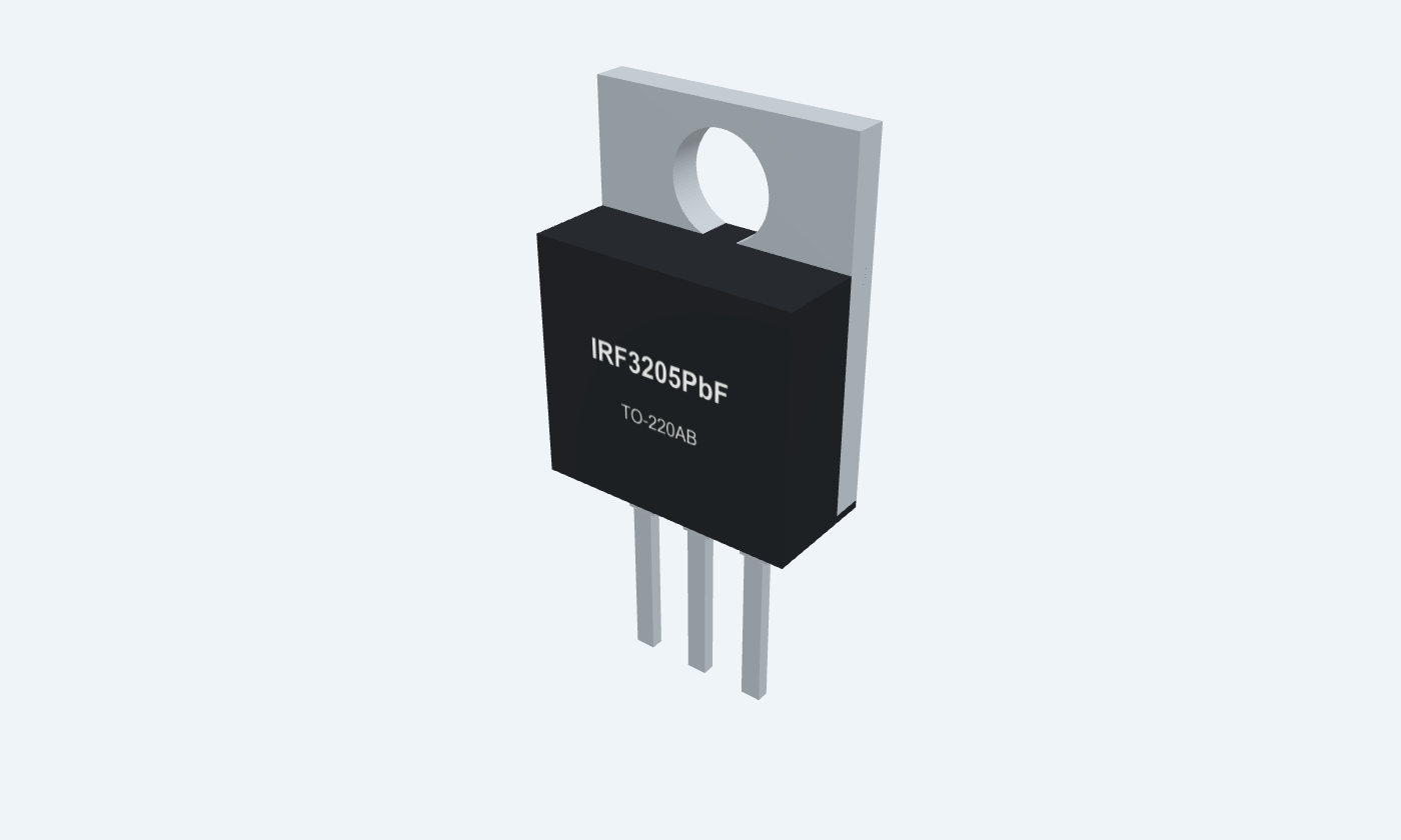
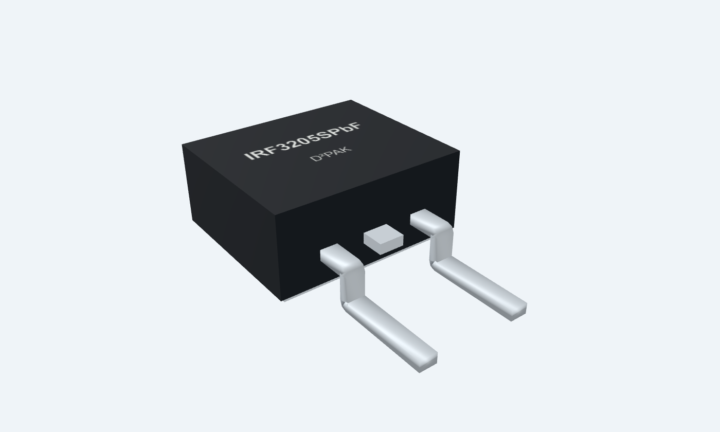
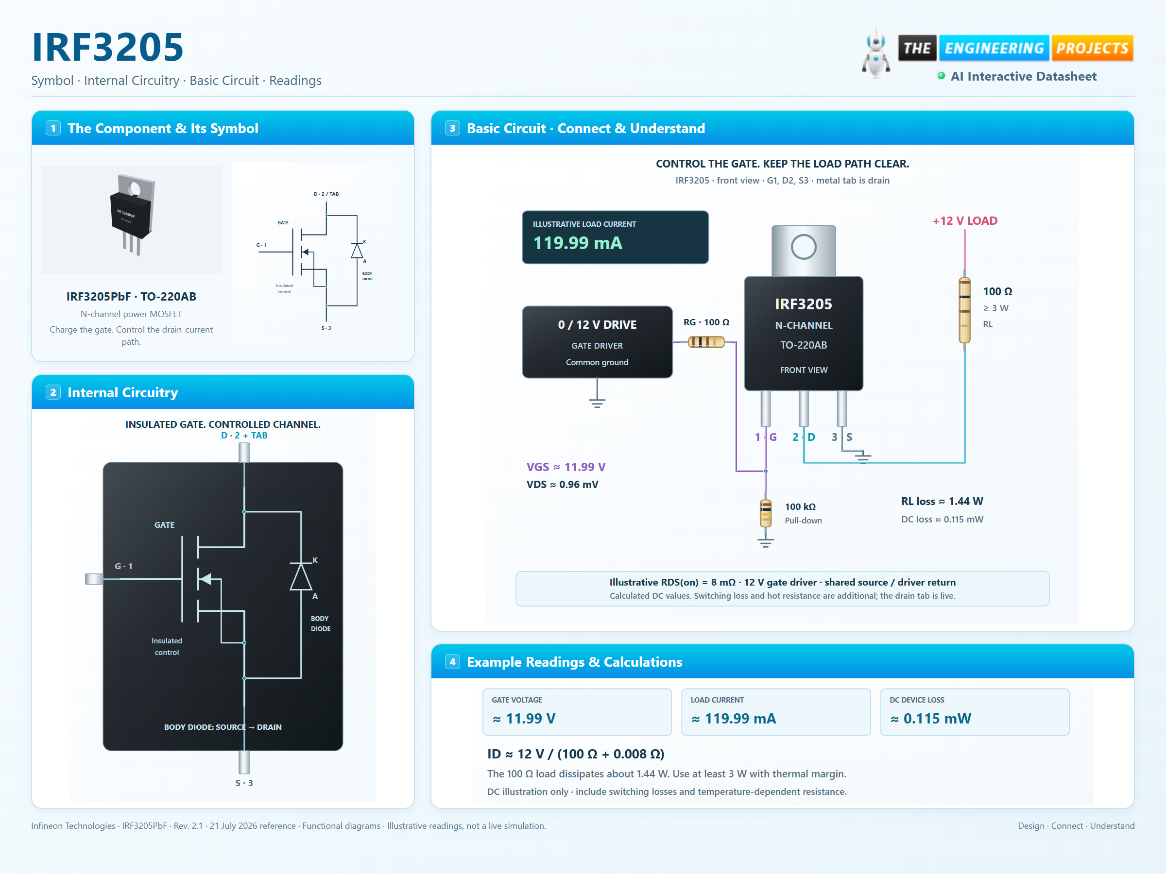
TO-220ABIRF3205PbF · Rev. 2.1 · 21 July 2026IRF3205 is a 55 V N-channel power MOSFET. Its insulated gate controls the drain-source channel, and its 8 mΩ maximum on-resistance is specified with 10 V gate drive. The 2–4 V threshold only marks the start of conduction at 250 µA; it is not a full-on logic-drive specification. IRF3205PbF uses a through-hole TO-220 package. The separately documented IRF3205SPbF uses D2PAK surface mounting. Both use gate 1, drain 2 and source 3, with the metal tab or thermal pad connected to drain. Their physical views and PCB patterns follow the selected package. A modest 12 V resistor-load example separates the gate-driver and load paths. The headline 110 A is a calculated silicon limit; the manufacturer explicitly limits the package to 75 A. Safe operating area, hot resistance and switching loss still constrain the usable current.
Select a pin to explore its connection
Click a lead or use the arrow keys. Front view · G1, D2, S3 · tab = D
Insulated control terminal that must be charged and discharged.
Use a gate driver, series resistor and gate-to-source pull-down.
Threshold is 2–4 V at only 250 µA. The 8 mΩ maximum on-resistance is specified at 10 V gate drive and 62 A, not at 3.3 V logic.
Connects to the controlled load in a low-side N-channel switch.
Place the load between its positive supply and drain pin 2.
The exposed metal tab is drain. The body diode has its cathode at drain.
Return terminal and reference for gate voltage.
Connect to common ground in the pictured low-side circuit.
The body diode has its anode at source. Keep the driver return close to this terminal.
Use a suitable gate driver: 8 mΩ is specified at VGS 10 V, not at the threshold. Check safe operating area, actual cooling and transient gate current.
IRF3205PbF · TO-220AB
| Property | Details |
|---|---|
| Manufacturer | Infineon Technologies |
| Part number | IRF3205PbF |
| Package | TO-220AB |
| Connections | 3 pins |
| Mounting | Through-hole |
| Lead pitch | 2.54 mm |
| Package code | TO-220 |
| Thermal reference | 200 W at case 25°C; not a free-air rating |
Two manufacturer-hosted references
Scroll sideways to see all columns.
| Parameter | Value | Conditions / notes |
|---|---|---|
| Through-hole | IRF3205PbF · TO-220AB | Rev. 2.1 · 21 July 2026 |
| Surface-mount | IRF3205SPbF · D2PAK | PD95106 · 11 March 2004 |
| Physical terminals | G1 · D2 · S3 | Tab and thermal pad are electrically drain |
| Gate drive | RDS(on) specified at 10 V | No guaranteed 3.3 V / 5 V on-resistance in these references |
| Mounting | Through-hole or surface-mount as selected | Do not surface-mount the TO-220 leads as if they were D2PAK |
No specifications match. Try a parameter name or a unit.
Review exact orderable availability separately from this reference.
Case temperature and pulse conditions matter
Scroll sideways to see all columns.
| Parameter | Value | Conditions / notes |
|---|---|---|
| Drain-source breakdown | 55 V minimum | VGS 0 V; ID 250 µA |
| Continuous current at 25 / 100°C case | 110 / 80 A | VGS 10 V; apply package limit and SOA |
| Package current limit | 75 A | 110 A is calculated from junction temperature; package limit remains binding |
| Pulsed drain current | 390 A | Pulse width limited by junction temperature |
| Case-cooled power | 200 W | Case at 25°C |
| Power derating | 1.3 W/°C | Above 25°C case temperature |
| Gate-source limit | ±20 V | Absolute maximum |
| Junction / storage | −55 to +175°C | Absolute ranges |
No specifications match. Try a parameter name or a unit.
Do not combine individual maximum ratings into one operating point.
25°C; pulse ≤400 µs and duty ≤2% where specified
Scroll sideways to see all columns.
| Parameter | Value | Conditions / notes |
|---|---|---|
| On-resistance | 8 mΩ maximum | VGS 10 V; ID 62 A |
| Gate threshold | 2–4 V | VDS = VGS; ID 250 µA |
| Transconductance | 44 S minimum | VDS 25 V; ID 62 A |
| Drain leakage | 25 µA maximum | VDS 55 V; VGS 0 V |
| Hot drain leakage | 250 µA maximum | VDS 44 V; VGS 0 V; TJ 150°C |
| Gate leakage | ±100 nA maximum | VGS ±20 V |
No specifications match. Try a parameter name or a unit.
Temperature-dependent resistance must be considered in a real load stage.
Explicit driver and load test conditions
Scroll sideways to see all columns.
| Parameter | Value | Conditions / notes |
|---|---|---|
| Qg / Qgs / Qgd | 146 / 35 / 54 nC maximum | ID 62 A; VDS 44 V; VGS 10 V |
| Delay-on / rise / delay-off / fall | 14 / 101 / 50 / 65 ns typical | VDD 28 V; ID 62 A; RG 4.5 Ω; VGS 10 V |
| Ciss / Coss / Crss | 3247 / 781 / 211 pF typical | VGS 0 V; VDS 25 V; 1 MHz |
| Drive requirement | Source and sink gate charge | A threshold voltage does not describe gate-drive current |
No specifications match. Try a parameter name or a unit.
Different gate resistance and load conditions produce different switching waveforms.
Selected references use separate ambient conditions
Scroll sideways to see all columns.
| Parameter | Value | Conditions / notes |
|---|---|---|
| Body diode | Anode source; cathode drain | Intrinsic reverse-current path |
| Forward drop | 1.3 V maximum | IS 62 A; VGS 0 V; TJ 25°C |
| Recovery time typical / maximum | 69 / 104 ns | IF 62 A; di/dt 100 A/µs |
| Recovery charge typical / maximum | 143 / 215 nC | Same recovery conditions |
| Junction-to-case | 0.75°C/W maximum | Both selected references |
| TO-220 junction-to-ambient | 62°C/W maximum | Manufacturer reference condition |
| D2PAK junction-to-ambient | 40°C/W maximum | Mounted on 1-inch-square FR-4 / G-10 PCB |
| Case-to-sink | 0.50°C/W typical | TO-220 flat, greased interface |
No specifications match. Try a parameter name or a unit.
A case-cooled power rating is not a free-air rating.
Illustrative constant-resistance model
Scroll sideways to see all columns.
| Parameter | Value | Conditions / notes |
|---|---|---|
| Load / source return | 100 Ω, at least 3 W / common ground | Supply to drain; source to ground |
| Gate driver | 0 / 12 V push-pull output | 100 Ω series gate resistor; 100 kΩ gate-source pull-down |
| Steady gate voltage | About 11.99 V | Divider included; ideal driver and negligible leakage |
| Channel resistance | 8 mΩ | Teaching model using the published 25°C maximum test point |
| Load current / channel drop | 119.99 mA / 0.96 mV | 12/(100+RDS); I × RDS |
| Channel / load loss | 0.115 mW / 1.440 W | I²R; switching and hot-resistance losses omitted |
| Inductive load | Needs its own flyback path | The pictured resistor is not an inductive load |
No specifications match. Try a parameter name or a unit.
These are calculated values, not measured or live simulation readings.
Select a pin for its function, connection guidance and electrical notes.
Follow the labeled connections and functional stages
3 stages · Explore one step at a time
The driver supplies current through the gate resistor during transitions.
Sufficient positive gate-to-source voltage enables the drain-source current path.
The driver removes gate charge; the pull-down defines the off state when the driver is inactive.
Separate gate driver and load paths keep the connections clear.
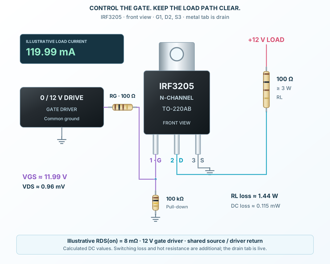
Follow the component values and pin connections
Place the 100 Ω resistor between +12 V and drain.
Drive gate from 0 / 12 V through 100 Ω.
Connect source and driver return to the common ground.
A compact functional view inside the device.
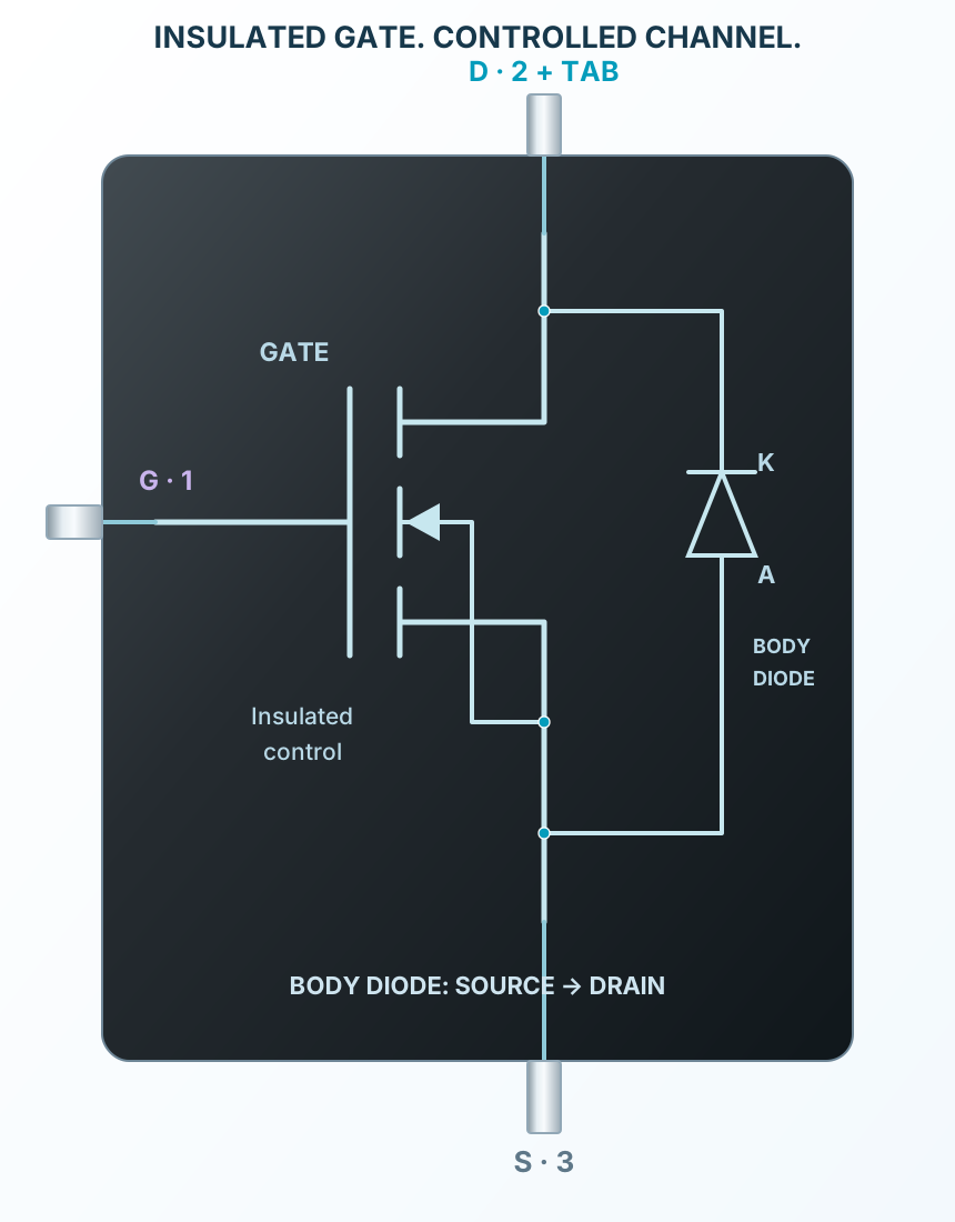
Select a stage to see its role and connections
No conductive DC path through the ideal gate oxide.
Positive VGS enables the N-channel path.
The diode’s anode is source and cathode is drain.
Signal names, electrical functions and connection guidance
Scroll within the table to see all columns and rows.
| Pin | Signal | Type | Function & connection |
|---|---|---|---|
| G | Gate | Insulated control terminal that must be charged and discharged.Connection guidanceUse a gate driver, series resistor and gate-to-source pull-down. Threshold is 2–4 V at only 250 µA. The 8 mΩ maximum on-resistance is specified at 10 V gate drive and 62 A, not at 3.3 V logic. | |
| D | Drain | Connects to the controlled load in a low-side N-channel switch.Connection guidancePlace the load between its positive supply and drain pin 2. The exposed metal tab is drain. The body diode has its cathode at drain. | |
| S | Source | Return terminal and reference for gate voltage.Connection guidanceConnect to common ground in the pictured low-side circuit. The body diode has its anode at source. Keep the driver return close to this terminal. |
No pins match these filters. Try another signal name or reset the filters.
Two manufacturer-hosted references
Scroll within the table to see all columns and rows.
| Parameter | Value | Conditions / notes |
|---|---|---|
| Through-hole | IRF3205PbF · TO-220AB | Rev. 2.1 · 21 July 2026 |
| Surface-mount | IRF3205SPbF · D2PAK | PD95106 · 11 March 2004 |
| Physical terminals | G1 · D2 · S3 | Tab and thermal pad are electrically drain |
| Gate drive | RDS(on) specified at 10 V | No guaranteed 3.3 V / 5 V on-resistance in these references |
| Mounting | Through-hole or surface-mount as selected | Do not surface-mount the TO-220 leads as if they were D2PAK |
No specifications match. Try a parameter name or a unit.
Review exact orderable availability separately from this reference.
Case temperature and pulse conditions matter
Scroll within the table to see all columns and rows.
| Parameter | Value | Conditions / notes |
|---|---|---|
| Drain-source breakdown | 55 V minimum | VGS 0 V; ID 250 µA |
| Continuous current at 25 / 100°C case | 110 / 80 A | VGS 10 V; apply package limit and SOA |
| Package current limit | 75 A | 110 A is calculated from junction temperature; package limit remains binding |
| Pulsed drain current | 390 A | Pulse width limited by junction temperature |
| Case-cooled power | 200 W | Case at 25°C |
| Power derating | 1.3 W/°C | Above 25°C case temperature |
| Gate-source limit | ±20 V | Absolute maximum |
| Junction / storage | −55 to +175°C | Absolute ranges |
No specifications match. Try a parameter name or a unit.
Do not combine individual maximum ratings into one operating point.
25°C; pulse ≤400 µs and duty ≤2% where specified
Scroll within the table to see all columns and rows.
| Parameter | Value | Conditions / notes |
|---|---|---|
| On-resistance | 8 mΩ maximum | VGS 10 V; ID 62 A |
| Gate threshold | 2–4 V | VDS = VGS; ID 250 µA |
| Transconductance | 44 S minimum | VDS 25 V; ID 62 A |
| Drain leakage | 25 µA maximum | VDS 55 V; VGS 0 V |
| Hot drain leakage | 250 µA maximum | VDS 44 V; VGS 0 V; TJ 150°C |
| Gate leakage | ±100 nA maximum | VGS ±20 V |
No specifications match. Try a parameter name or a unit.
Temperature-dependent resistance must be considered in a real load stage.
Explicit driver and load test conditions
Scroll within the table to see all columns and rows.
| Parameter | Value | Conditions / notes |
|---|---|---|
| Qg / Qgs / Qgd | 146 / 35 / 54 nC maximum | ID 62 A; VDS 44 V; VGS 10 V |
| Delay-on / rise / delay-off / fall | 14 / 101 / 50 / 65 ns typical | VDD 28 V; ID 62 A; RG 4.5 Ω; VGS 10 V |
| Ciss / Coss / Crss | 3247 / 781 / 211 pF typical | VGS 0 V; VDS 25 V; 1 MHz |
| Drive requirement | Source and sink gate charge | A threshold voltage does not describe gate-drive current |
No specifications match. Try a parameter name or a unit.
Different gate resistance and load conditions produce different switching waveforms.
Selected references use separate ambient conditions
Scroll within the table to see all columns and rows.
| Parameter | Value | Conditions / notes |
|---|---|---|
| Body diode | Anode source; cathode drain | Intrinsic reverse-current path |
| Forward drop | 1.3 V maximum | IS 62 A; VGS 0 V; TJ 25°C |
| Recovery time typical / maximum | 69 / 104 ns | IF 62 A; di/dt 100 A/µs |
| Recovery charge typical / maximum | 143 / 215 nC | Same recovery conditions |
| Junction-to-case | 0.75°C/W maximum | Both selected references |
| TO-220 junction-to-ambient | 62°C/W maximum | Manufacturer reference condition |
| D2PAK junction-to-ambient | 40°C/W maximum | Mounted on 1-inch-square FR-4 / G-10 PCB |
| Case-to-sink | 0.50°C/W typical | TO-220 flat, greased interface |
No specifications match. Try a parameter name or a unit.
A case-cooled power rating is not a free-air rating.
Illustrative constant-resistance model
Scroll within the table to see all columns and rows.
| Parameter | Value | Conditions / notes |
|---|---|---|
| Load / source return | 100 Ω, at least 3 W / common ground | Supply to drain; source to ground |
| Gate driver | 0 / 12 V push-pull output | 100 Ω series gate resistor; 100 kΩ gate-source pull-down |
| Steady gate voltage | About 11.99 V | Divider included; ideal driver and negligible leakage |
| Channel resistance | 8 mΩ | Teaching model using the published 25°C maximum test point |
| Load current / channel drop | 119.99 mA / 0.96 mV | 12/(100+RDS); I × RDS |
| Channel / load loss | 0.115 mW / 1.440 W | I²R; switching and hot-resistance losses omitted |
| Inductive load | Needs its own flyback path | The pictured resistor is not an inductive load |
No specifications match. Try a parameter name or a unit.
These are calculated values, not measured or live simulation readings.
No matching rowsTry a pin name, parameter, unit or test condition, or reset the filters.
Use adequate gate drive and a controlled thermal path.
Manufacturer application guideCheck charge, recovery and switching loss as well as conduction resistance.
Manufacturer application guideProvide appropriate flyback paths and transient protection.
Manufacturer application guideFind IRF3205 in the Components Library to place its schematic symbol and connect its pins.
Reference page · circuit simulation model not yet availableOpen ProTech