LM1117-3.3Fixed 3.3 V LDO regulator
A 3.3 V rail, with stability designed in.
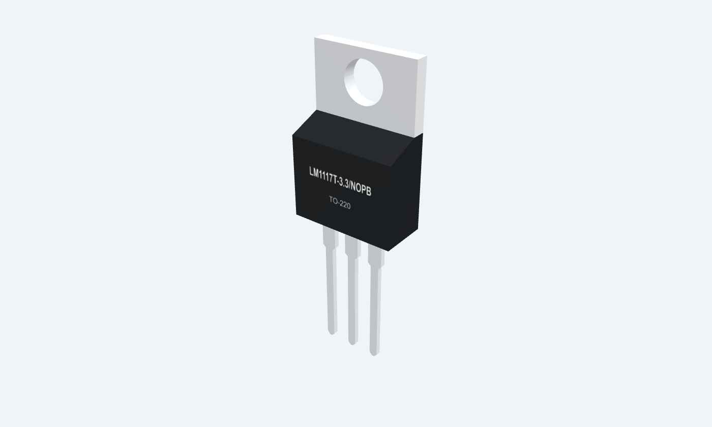
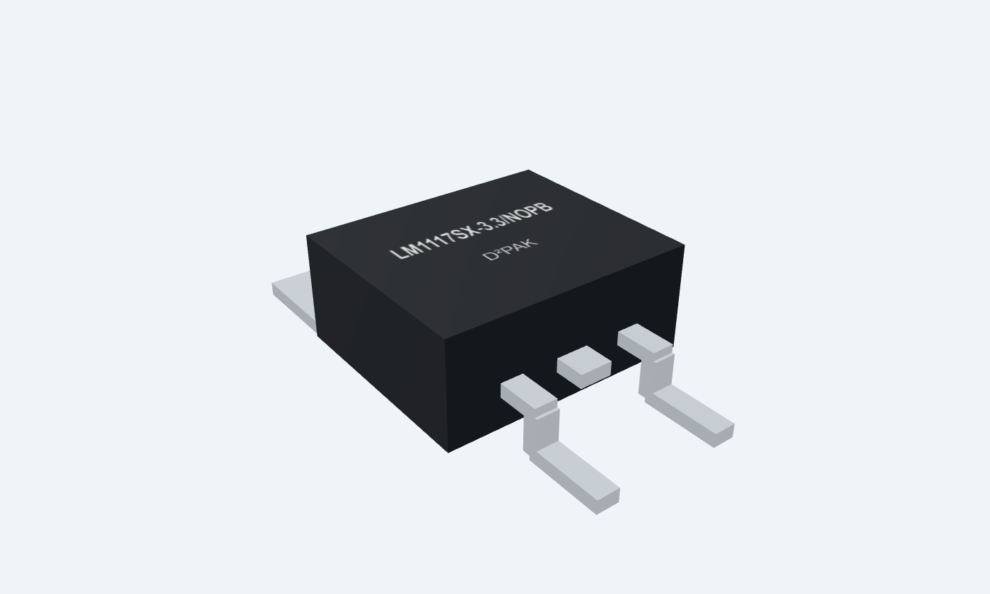
LM1117-3.3 is a three-terminal low-dropout linear regulator with a fixed 3.3 V output. This reference follows Texas Instruments LM1117 devices in TO-220 and D²PAK packages, using pin 1 GND, pin 2 OUTPUT and pin 3 INPUT. An internal reference and feedback divider control the pass stage. The metal tab is connected to OUTPUT, and the external output capacitor must satisfy both capacitance and ESR requirements. A 5 V source is convenient for a 3.3 V rail, but the voltage difference becomes heat. Check input headroom, load current and cooling together; the 800 mA rating is conditional on the operating limits.

3Physical pins
LM1117T-3.3/NOPBTO-220
Manufacturer-referencedTexas Instruments
Pin diagram
Select a pin to explore its connection
Highlight
LM1117-3.3TO-220Front view · marking toward you · leads down
LM1117-3.3D²PAKTop view · thermal tab is pin 2 (OUTPUT)
Click a lead or use the arrow keys. Front view · marking toward you · leads down
PIN 1 · Ground
Ground referenceGND
Function
Return for the internal reference, feedback divider and bias current in the fixed 3.3 V version.
How to connect
Connect to the input-supply return, load return and both capacitor returns.
Electrical note
This is GND on the fixed-output part. The adjustable LM1117 uses this lead as ADJ and is a different circuit.
PIN 2 · Output & tab
Regulated outputOUTPUT
Function
Supplies the nominal 3.3 V rail. The metal tab is electrically connected to this output.
How to connect
Connect the load and a suitable output capacitor close to the regulator.
Electrical note
The output capacitor is part of the stability requirements: TI specifies at least 10 µF tantalum with ESR from 0.3 Ω to 22 Ω. The tab is not ground.
PIN 3 · Supply
DC inputINPUT
Function
Feeds the pass stage and bias circuit from a supply above the output by sufficient headroom.
How to connect
Use a regulated 5 V source for the example and a local 10 µF input bypass.
Electrical note
Check input tolerance, ripple and dropout at the intended load and temperature. The 20 V absolute maximum is not the 15 V recommended maximum.
Key specifications
The fixed-output feedback divider is inside the package. External capacitors and a good thermal path complete the supply.
Fixed output3.3 V nominal
Rated output current800 mA · thermal limits apply
Operating junction0–125 °C · selected LM1117 grade
Output capacitor≥ 10 µF tantalum · check ESR
Package details
LM1117T-3.3/NOPB · TO-220
| Property | Details |
|---|---|
| Manufacturer | Texas Instruments |
| Part number | LM1117T-3.3/NOPB |
| Package | TO-220 |
| Connections | 3 pins |
| Mounting | Through-hole |
| Lead pitch | 2.54 mm |
| Package code | NDE |
| Thermal reference | Board and heatsink dependent; see TI SNOS412Q |
Operating characteristics
TI LM1117-3.3 · fixed-output grade
Manufacturer specifications 6 parameters
Scroll sideways to see all columns.
| Parameter | Value | Conditions / notes |
|---|---|---|
| Nominal output | 3.3 V | Fixed 3.3 V option |
| Output at 25°C | 3.267 / 3.3 / 3.333 V | Minimum / typical / maximum; VIN = 5 V, IOUT = 10 mA |
| Output across specified conditions | 3.235–3.365 V | 0–800 mA; VIN = 4.75–10 V; TJ = 0–125°C |
| Output current | Up to 800 mA | Requires headroom and adequate thermal design |
| Junction operating range | 0–125°C | Selected LM1117 grade |
| Recommended input maximum | 15 V | Must also satisfy thermal and dropout constraints |
No specifications match. Try a parameter name or a unit.
The LM1117I grade has a different temperature range. This reference follows the selected non-I devices.
Regulation and supply current
Retain the measurement conditions
Manufacturer specifications 5 parameters
Scroll sideways to see all columns.
| Parameter | Value | Conditions / notes |
|---|---|---|
| Line regulation | 1 mV typical; 6 mV maximum | IOUT = 0 mA, VIN = 4.75–15 V; typical at 25°C, maximum over 0–125°C |
| Load regulation | 1 mV typical; 10 mV maximum | VIN = 4.75 V, IOUT = 0–800 mA; typical at 25°C, maximum over 0–125°C |
| Ground current | 5 mA typical; 10 mA maximum | VIN ≤ 15 V; typical at 25°C, maximum over 0–125°C |
| Dropout criterion | Output falls by 100 mV | Referenced to VOUT measured with VIN = VOUT + 1.5 V |
| Current limiting | Built in | An overload protection feature, not an extra operating-current allowance |
No specifications match. Try a parameter name or a unit.
Dropout changes with output current and junction temperature; use TI’s table and curves when choosing the supply margin.
Capacitors and stability
Capacitance and ESR both matter
Manufacturer specifications 5 parameters
Scroll sideways to see all columns.
| Parameter | Value | Conditions / notes |
|---|---|---|
| Input bypass | 10 µF tantalum | TI’s suitable input capacitor for most applications |
| Output capacitor | At least 10 µF tantalum | Required for the selected fixed-output circuit |
| Output capacitor ESR | 0.3–22 Ω | Manufacturer stability guidance |
| Low-ESR substitution | Check before changing technology | A ceramic capacitor is not automatically a valid drop-in replacement |
| Placement | Short input, output and ground paths | Keep the load return and regulator ground well connected |
No specifications match. Try a parameter name or a unit.
Check capacitance, ESR, voltage rating and temperature behavior for the actual capacitor part.
5 V to 3.3 V example
100 mA nominal resistive load
Manufacturer specifications 6 parameters
Scroll sideways to see all columns.
| Parameter | Value | Conditions / notes |
|---|---|---|
| Supply | Regulated 5 V DC | Feed pin 3 INPUT |
| Return | Pin 1 GND | Common with input supply, capacitors and load |
| Output | Pin 2 OUTPUT | Nominal 3.3 V; tab is the same net |
| Example load | 33 Ω · at least 1 W | 3.3 / 33 = 0.10 A; resistor power = 0.33 W |
| Pass-stage loss | 0.17 W | (5 − 3.3) × 0.10 |
| Including typical ground current | Approximately 0.195 W | 0.17 + 5 × 0.005 |
No specifications match. Try a parameter name or a unit.
These are nominal calculations, not measured results. Output tolerance and actual ground current change the values.
Thermal and stress limits
Package ratings require a thermal context
Manufacturer specifications 7 parameters
Scroll sideways to see all columns.
| Parameter | Value | Conditions / notes |
|---|---|---|
| Power estimate | PD ≈ (VIN − VOUT) × ILOAD + VIN × IGND | Include both loss terms |
| Junction estimate | TJ ≈ TA + PD × RθJA | Only for the board and airflow represented by the thermal resistance |
| TO-220 RθJA / RθJC(bottom) | 23.8 / 1.5°C/W | TI thermal characterization conditions |
| D²PAK RθJA / RθJC(bottom) | 41.3 / 1.3°C/W | TI thermal characterization conditions |
| Input absolute maximum | 20 V | Stress rating, not the recommended operating maximum |
| Junction absolute maximum | 150°C | Recommended operation ends at 125°C |
| Storage range | −65 to +150°C | Unpowered |
No specifications match. Try a parameter name or a unit.
The output-connected tab must not be shorted to a grounded heatsink. Thermal shutdown does not replace cooling design.
Connections by function
Select a pin for its function, connection guidance and electrical notes.
Ground1 pin
Output & tab1 pin
Supply1 pin
Ground1 pin
Output & tab1 pin
Supply1 pin
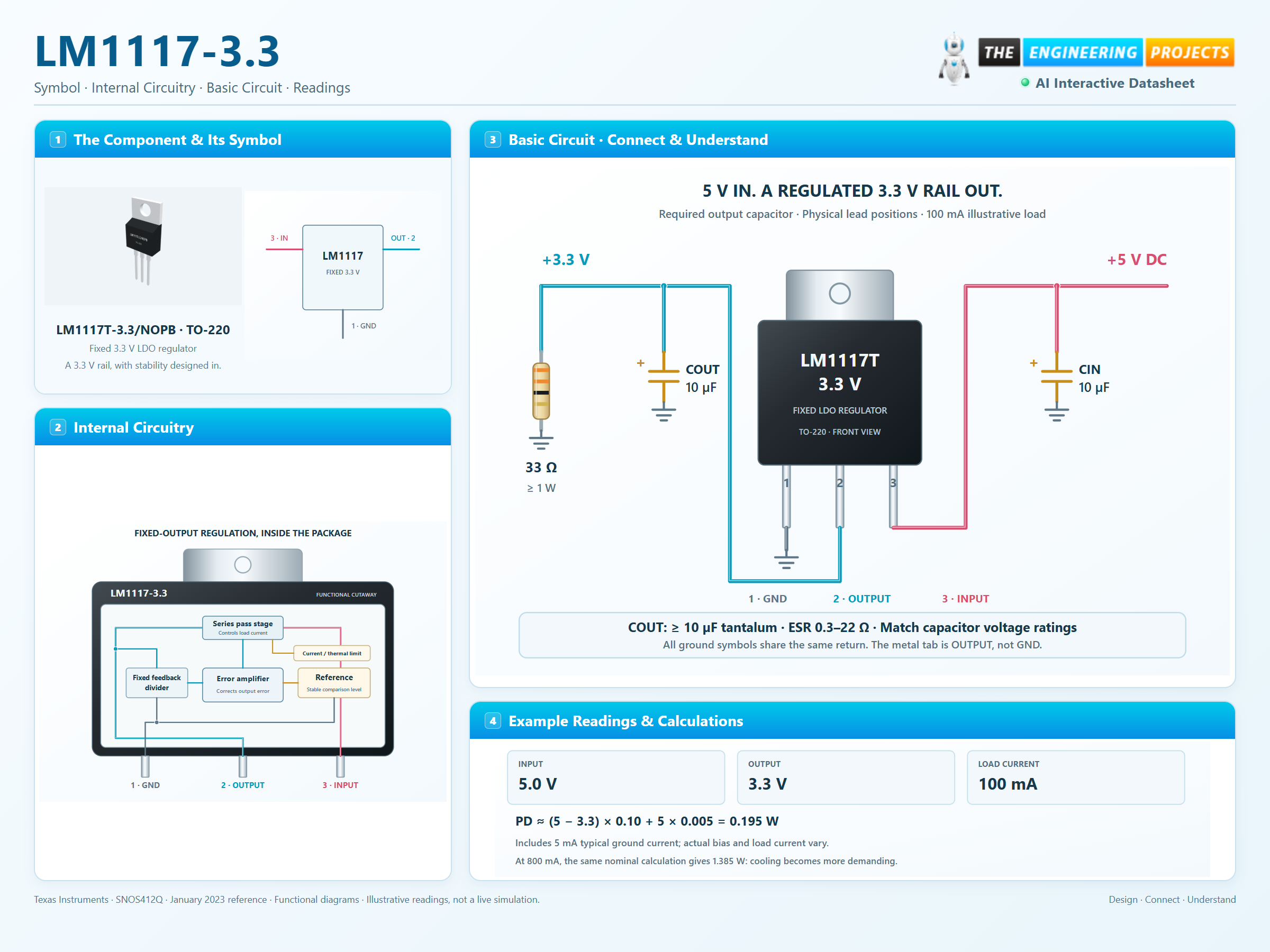
LM1117-3.3 at a glance
Follow the labeled connections and functional stages
How it works
3 stages · Explore one step at a time
Compare and regulate
A reference and internal feedback network set the fixed 3.3 V output. The amplifier adjusts the pass stage as input or load changes.
Stabilize the feedback loop
The output capacitor is required, not merely decorative bypassing. Select its capacitance and ESR for the manufacturer’s operating conditions.
Account for power loss
The voltage dropped across the pass stage produces heat. Ground current adds another loss term, and the package needs a suitable thermal path.
Step 1 of 3
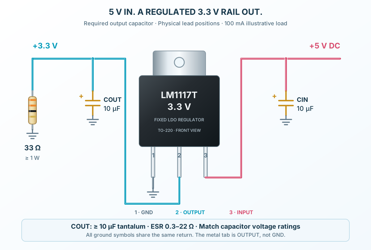
LM1117-3.3 in a circuit
Physical lead positions, local capacitors and a visible load.
Connect it, step by step
Follow the component values and pin connections
Feed INPUT
Connect regulated 5 V to lead 3 and place the input bypass nearby.
Connect OUTPUT and GND
Lead 2 and the tab are output. Lead 1 is ground. Add the required output capacitor and common load return.
Check the load
The 33 Ω example load draws about 100 mA and dissipates 0.33 W. Confirm regulator temperature under the actual cooling conditions.
Inside LM1117-3.3
A compact fixed-output feedback loop inside the package.
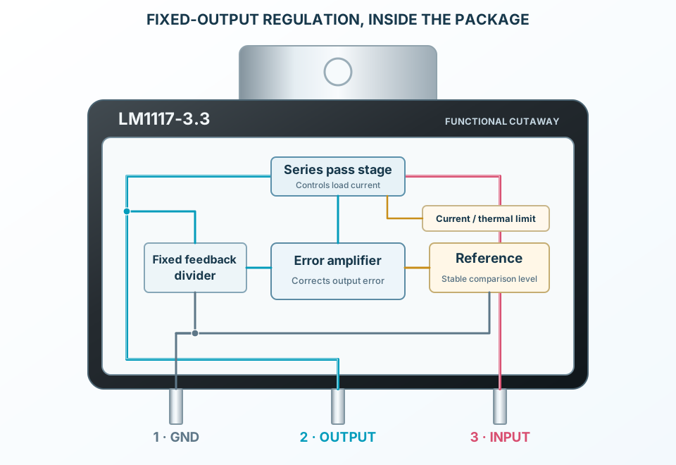
Explore the circuit
Select a stage to see its role and connections
Internal set point
The fixed-output part includes the feedback network that sets 3.3 V.
Feedback correction
The amplifier changes pass-stage drive to oppose output disturbances while headroom remains.
External loop support
The output capacitor and its ESR affect the stability of this control loop.
Selected packageTO-220LM1117T-3.3/NOPB
Physical connections3 pinsPackage-specific numbering
Reference collection6 tables29 parameters & pin functions
Pin reference
Signal names, electrical functions and connection guidance
Physical pin numbers3 pins
Scroll within the table to see all columns and rows.
| Pin | Signal | Type | Function & connection |
|---|---|---|---|
| GND | Ground reference | Return for the internal reference, feedback divider and bias current in the fixed 3.3 V version.Connection guidanceConnect to the input-supply return, load return and both capacitor returns. This is GND on the fixed-output part. The adjustable LM1117 uses this lead as ADJ and is a different circuit. | |
| OUTPUT | Regulated output | Supplies the nominal 3.3 V rail. The metal tab is electrically connected to this output.Connection guidanceConnect the load and a suitable output capacitor close to the regulator. The output capacitor is part of the stability requirements: TI specifies at least 10 µF tantalum with ESR from 0.3 Ω to 22 Ω. The tab is not ground. | |
| INPUT | DC input | Feeds the pass stage and bias circuit from a supply above the output by sufficient headroom.Connection guidanceUse a regulated 5 V source for the example and a local 10 µF input bypass. Check input tolerance, ripple and dropout at the intended load and temperature. The 20 V absolute maximum is not the 15 V recommended maximum. |
No pins match these filters. Try another signal name or reset the filters.
Operating characteristics
TI LM1117-3.3 · fixed-output grade
Manufacturer-referenced values6 parameters
Scroll within the table to see all columns and rows.
| Parameter | Value | Conditions / notes |
|---|---|---|
| Nominal output | 3.3 V | Fixed 3.3 V option |
| Output at 25°C | 3.267 / 3.3 / 3.333 V | Minimum / typical / maximum; VIN = 5 V, IOUT = 10 mA |
| Output across specified conditions | 3.235–3.365 V | 0–800 mA; VIN = 4.75–10 V; TJ = 0–125°C |
| Output current | Up to 800 mA | Requires headroom and adequate thermal design |
| Junction operating range | 0–125°C | Selected LM1117 grade |
| Recommended input maximum | 15 V | Must also satisfy thermal and dropout constraints |
No specifications match. Try a parameter name or a unit.
The LM1117I grade has a different temperature range. This reference follows the selected non-I devices.
Regulation and supply current
Retain the measurement conditions
Manufacturer-referenced values5 parameters
Scroll within the table to see all columns and rows.
| Parameter | Value | Conditions / notes |
|---|---|---|
| Line regulation | 1 mV typical; 6 mV maximum | IOUT = 0 mA, VIN = 4.75–15 V; typical at 25°C, maximum over 0–125°C |
| Load regulation | 1 mV typical; 10 mV maximum | VIN = 4.75 V, IOUT = 0–800 mA; typical at 25°C, maximum over 0–125°C |
| Ground current | 5 mA typical; 10 mA maximum | VIN ≤ 15 V; typical at 25°C, maximum over 0–125°C |
| Dropout criterion | Output falls by 100 mV | Referenced to VOUT measured with VIN = VOUT + 1.5 V |
| Current limiting | Built in | An overload protection feature, not an extra operating-current allowance |
No specifications match. Try a parameter name or a unit.
Dropout changes with output current and junction temperature; use TI’s table and curves when choosing the supply margin.
Capacitors and stability
Capacitance and ESR both matter
Manufacturer-referenced values5 parameters
Scroll within the table to see all columns and rows.
| Parameter | Value | Conditions / notes |
|---|---|---|
| Input bypass | 10 µF tantalum | TI’s suitable input capacitor for most applications |
| Output capacitor | At least 10 µF tantalum | Required for the selected fixed-output circuit |
| Output capacitor ESR | 0.3–22 Ω | Manufacturer stability guidance |
| Low-ESR substitution | Check before changing technology | A ceramic capacitor is not automatically a valid drop-in replacement |
| Placement | Short input, output and ground paths | Keep the load return and regulator ground well connected |
No specifications match. Try a parameter name or a unit.
Check capacitance, ESR, voltage rating and temperature behavior for the actual capacitor part.
5 V to 3.3 V example
100 mA nominal resistive load
Manufacturer-referenced values6 parameters
Scroll within the table to see all columns and rows.
| Parameter | Value | Conditions / notes |
|---|---|---|
| Supply | Regulated 5 V DC | Feed pin 3 INPUT |
| Return | Pin 1 GND | Common with input supply, capacitors and load |
| Output | Pin 2 OUTPUT | Nominal 3.3 V; tab is the same net |
| Example load | 33 Ω · at least 1 W | 3.3 / 33 = 0.10 A; resistor power = 0.33 W |
| Pass-stage loss | 0.17 W | (5 − 3.3) × 0.10 |
| Including typical ground current | Approximately 0.195 W | 0.17 + 5 × 0.005 |
No specifications match. Try a parameter name or a unit.
These are nominal calculations, not measured results. Output tolerance and actual ground current change the values.
Thermal and stress limits
Package ratings require a thermal context
Manufacturer-referenced values7 parameters
Scroll within the table to see all columns and rows.
| Parameter | Value | Conditions / notes |
|---|---|---|
| Power estimate | PD ≈ (VIN − VOUT) × ILOAD + VIN × IGND | Include both loss terms |
| Junction estimate | TJ ≈ TA + PD × RθJA | Only for the board and airflow represented by the thermal resistance |
| TO-220 RθJA / RθJC(bottom) | 23.8 / 1.5°C/W | TI thermal characterization conditions |
| D²PAK RθJA / RθJC(bottom) | 41.3 / 1.3°C/W | TI thermal characterization conditions |
| Input absolute maximum | 20 V | Stress rating, not the recommended operating maximum |
| Junction absolute maximum | 150°C | Recommended operation ends at 125°C |
| Storage range | −65 to +150°C | Unpowered |
No specifications match. Try a parameter name or a unit.
The output-connected tab must not be shorted to a grounded heatsink. Thermal shutdown does not replace cooling design.
No matching rowsTry a pin name, parameter, unit or test condition, or reset the filters.
Local logic rails
Supply a modest 3.3 V digital load from a regulated 5 V rail after checking load transients and heating.
Manufacturer application guidePost-regulation
Regulate a sufficiently higher DC rail near a load using the specified capacitor network.
Manufacturer application guidePower-supply learning
Explore dropout, capacitor ESR and the relationship between voltage drop and heat.
Manufacturer application guideTake it into ProTech
Find LM1117-3.3 in the Components Library to place its schematic symbol and connect its pins.
Reference page · circuit simulation model not yet availableOpen ProTech