LM13700Dual operational transconductance amplifier
Control an analog gain with a small bias current.
LM13700 contains two operational transconductance amplifiers, or OTAs. Each turns a small differential input voltage into an output current, with its conversion factor set by an external amplifier-bias current. An external load converts that current into a voltage. Input-linearizing diodes support wider signal ranges when correctly biased, and separate Darlington buffers can drive a following stage. These buffers need external connections and bias loads. This reference uses a ±15 V, low-amplitude bench circuit to make the gain-control principle visible. SOIC-16 is listed in the current ordering appendix; PDIP-16 is retained as the documented legacy LM13700N package. Both share the same 16-pin function map.
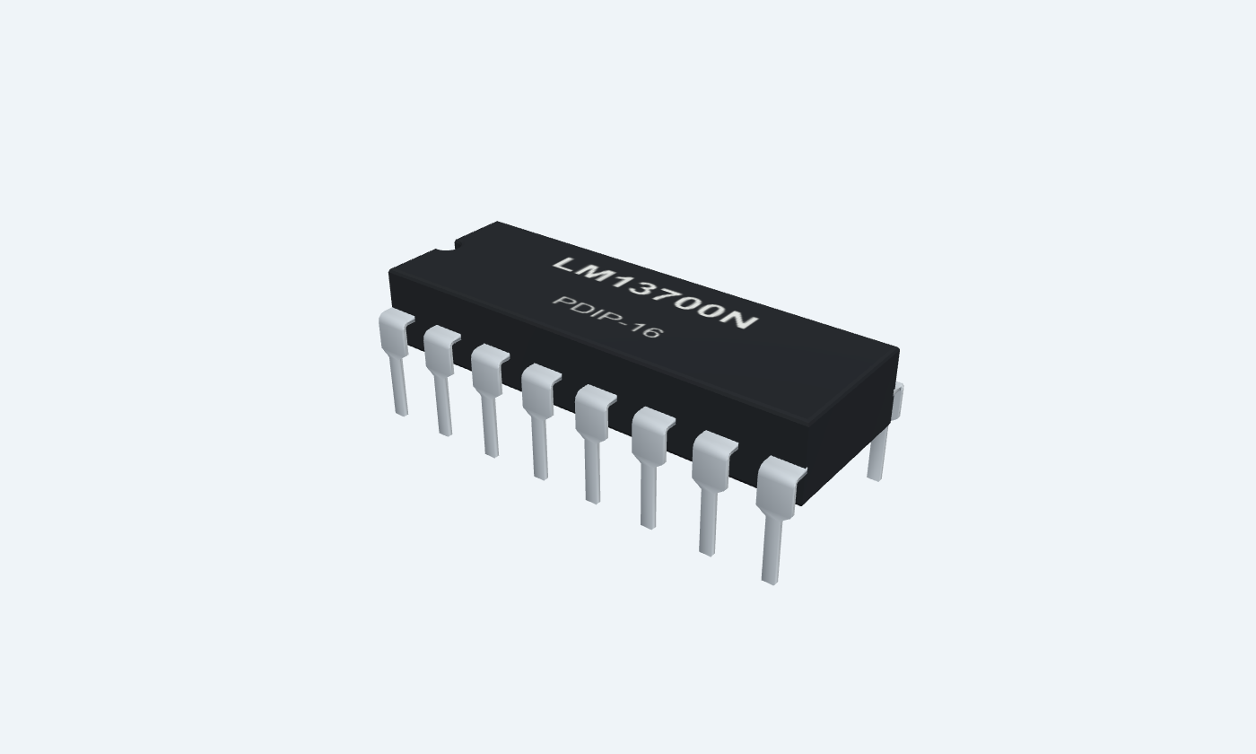
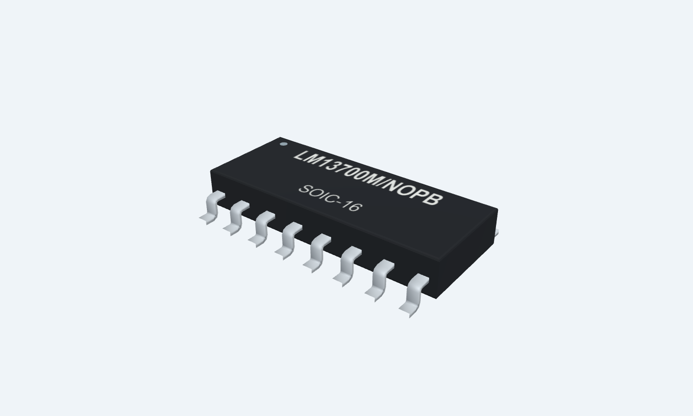

16Physical pins
LM13700NPDIP-16
Manufacturer-referencedTexas Instruments
Pin diagram
Select a pin to explore its connection
Highlight
LM13700NPDIP-16Top view
LM13700SOIC-16Top view
Click a lead or use the arrow keys. Top view
PIN 1 · Gain-control current
Channel A bias currentIABC A
Function
Sets channel A transconductance through an externally supplied current.
How to connect
For the example, connect a 150 kΩ resistor from circuit GND to this pin.
Electrical note
The pin sits approximately two diode drops above V−; do not drive it directly from a voltage source. Absolute maximum is 2 mA.
PIN 2 · Linearizing diodes
Channel A diode biasDIODE A
Function
Feeds the two input-linearizing diodes.
How to connect
Leave open in the small-signal example. Use a properly limited bias current when enabling the diodes.
Electrical note
The diode current and input attenuation must be designed together; 2 mA is an absolute maximum.
PIN 3 · Differential input
Channel A noninverting inputIN+ A
Function
A positive differential input produces positive output current.
How to connect
Apply a 1 kHz sine wave, ±2 mV peak, centered on circuit GND.
PIN 4 · Differential input
Channel A inverting inputIN− A
Function
The OTA responds to IN+ minus IN−.
How to connect
Connect to circuit GND in this example.
Electrical note
Keep the differential signal small when the linearizing diodes are unused.
PIN 5 · OTA current output
Channel A current outputOUT A
Function
High-impedance output supplies a current proportional to differential voltage.
How to connect
Connect a 10 kΩ load to GND and a high-impedance scope.
Electrical note
This is a current output, not an ordinary low-impedance voltage-amplifier output.
PIN 6 · Supply
Negative supplyV−
Function
Negative supply for both OTAs and buffers.
How to connect
Connect to −15 V and bypass to circuit GND with 100 nF.
PIN 7 · Independent buffers
Channel A buffer inputBUF IN A
Function
Independent input to the Darlington output buffer.
How to connect
Ground in this unbuffered example.
Electrical note
It is not internally connected to OUT A pin 5.
PIN 8 · Independent buffers
Channel A buffer outputBUF OUT A
Function
Emitter-follower output with a two-junction level shift.
How to connect
Leave open in this example. When used, provide a bias load toward V−.
Electrical note
Output current and package dissipation must stay within limits; the buffer is not rail-to-rail.
PIN 9 · Independent buffers
Channel B buffer outputBUF OUT B
Function
Independent Darlington follower output.
How to connect
Leave open in this example.
PIN 10 · Independent buffers
Channel B buffer inputBUF IN B
Function
Independent input to the second buffer.
How to connect
Connect to circuit GND in this example.
Electrical note
It is not internally connected to OUT B pin 12.
PIN 11 · Supply
Positive supplyV+
Function
Positive supply shared by both channels.
How to connect
Connect to +15 V and bypass to circuit GND with 100 nF.
PIN 12 · OTA current output
Channel B current outputOUT B
Function
Second high-impedance OTA output.
How to connect
Leave open in this channel-A example.
PIN 13 · Differential input
Channel B inverting inputIN− B
Function
Negative differential input of the second OTA.
How to connect
Connect to circuit GND when channel B is unused here.
PIN 14 · Differential input
Channel B noninverting inputIN+ B
Function
Positive differential input of the second OTA.
How to connect
Connect to circuit GND when channel B is unused here.
PIN 15 · Linearizing diodes
Channel B diode biasDIODE B
Function
Bias connection for channel B linearizing diodes.
How to connect
Leave open in this example.
PIN 16 · Gain-control current
Channel B bias currentIABC B
Function
Sets the second channel transconductance independently.
How to connect
Leave open so IABC B is zero in this example.
Electrical note
An unused bias pin does not require a direct connection to GND.
Key specifications
The OTA controls output current. A load resistor supplies the current-to-voltage conversion; the optional buffer is a separate stage.
Independent OTAs2 plus two separate buffers
Recommended total rail span9.5–32 V
Typical transconductance9.6 mS at IABC = 500 µA
Operating grade0–70 °C
Package details
LM13700N · PDIP-16
| Property | Details |
|---|---|
| Manufacturer | Texas Instruments |
| Part number | LM13700N |
| Package | PDIP-16 |
| Connections | 16 pins |
| Mounting | Through-hole |
| Lead pitch | 2.54 mm |
| Package code | PDIP-16 |
| Thermal reference | See operating and package limits |
Supplies and limits
Recommended conditions and absolute ratings
Manufacturer specifications 7 parameters
Scroll sideways to see all columns.
| Parameter | Value | Conditions / notes |
|---|---|---|
| Recommended total supply | 9.5–32 V | Single-supply configuration |
| Recommended split supplies | ±4.75 to ±16 V | Symmetric dual-supply configuration |
| Example supply | +15 V / GND / −15 V | 30 V total rail span |
| Operating temperature | 0 to +70°C | Commercial grade |
| Absolute supply limit | 36 V total / ±18 V | Stress limit, not the operating target |
| Absolute IABC / diode current | 2 mA each | External current limiting is required |
| Absolute buffer output current | 20 mA | Also constrained by package dissipation |
No specifications match. Try a parameter name or a unit.
Circuit GND is the midpoint of the split supply; it is not the V− pin.
OTA characteristics
±15 V, 25°C, IABC = 500 µA unless noted
Manufacturer specifications 8 parameters
Scroll sideways to see all columns.
| Parameter | Value | Conditions / notes |
|---|---|---|
| Forward transconductance | 6.7–13 mS; 9.6 mS typical | 5.4 mS minimum over specified temperature |
| Channel gm tracking | 0.3 dB typical | Manufacturer reference conditions |
| Input offset | 0.4 mV typical; 4 mV maximum | Manufacturer specified-temperature condition |
| Input bias current | 0.4 µA typical; 5 µA maximum | 1 µA typical / 8 µA maximum over temperature |
| Input resistance | 26 kΩ typical; 10 kΩ minimum | Reference test conditions |
| Common-mode input range | ±12 V minimum; ±13.5 V typical | With ±15 V rails |
| Peak output current | 500 µA typical; 350–650 µA | IABC = 500 µA, RL = 0 |
| Supply current | 2.6 mA typical | Both channels, IABC = 500 µA |
No specifications match. Try a parameter name or a unit.
Typical transconductance and example gain are not guaranteed exact values.
Signal behavior
OTA and buffer are different stages
Manufacturer specifications 7 parameters
Scroll sideways to see all columns.
| Parameter | Value | Conditions / notes |
|---|---|---|
| Small-signal equation | IOUT ≈ gm × (VIN+ − VIN−) | Without the linearizing diodes, use a few millivolts differential |
| Typical gm at 25°C | Approximately 19.2 × IABC | IABC in amperes gives gm in siemens |
| Current-to-voltage conversion | VOUT ≈ IOUT × RL | Valid while output swing and current remain in range |
| Open-loop bandwidth | 2 MHz typical | Not a guaranteed closed-loop bandwidth for every circuit |
| Slew rate | 50 V/µs typical | Unity-gain compensated test |
| Separate buffers | Darlington emitter followers | Input must be connected externally; output has a level shift |
| Buffer load | Bias toward V− when used | Manufacturer buffer test uses 5 kΩ to V− |
No specifications match. Try a parameter name or a unit.
The LM13700 is not a pin-compatible replacement for a conventional dual voltage op amp.
Small-signal gain experiment
One OTA with an unbuffered resistive output
Manufacturer specifications 8 parameters
Scroll sideways to see all columns.
| Parameter | Value | Conditions / notes |
|---|---|---|
| V+11 / V−6 | +15 V / −15 V | 100 nF bypass from each rail to GND |
| IABC A1 | 150 kΩ to GND | Approximately 90.7 µA at the assumed bias voltage |
| IN+ A3 / IN− A4 | ±2 mV sine / GND | 1 kHz, zero DC offset |
| OUT A5 | 10 kΩ to GND plus high-impedance scope | Scope input capacitance affects high-frequency response |
| DIODE A2 and B15 | Open | Linearizing diodes unused in this experiment |
| BUF IN A7 and B10 | GND | BUF OUT A8 and B9 left open |
| Unused channel B | IN−13 and IN+14 to GND | IABC B16 and OUT B12 open |
| All source returns | Circuit GND | The split-supply midpoint, not −15 V |
No specifications match. Try a parameter name or a unit.
This is an explanatory circuit, not a running simulation. Offset and bias currents may add a DC output offset.
Gain calculation
Nominal 25°C example
Manufacturer specifications 7 parameters
Scroll sideways to see all columns.
| Parameter | Value | Conditions / notes |
|---|---|---|
| Bias pin estimate | V− + 2 VBE ≈ −13.6 V | Assume VBE ≈ 0.7 V |
| Bias current | 13.6 V / 150 kΩ ≈ 90.7 µA | Resistor goes from GND to IABC A1 |
| Transconductance | 19.2 × 90.7 µA ≈ 1.74 mS | Typical small-signal approximation |
| Voltage gain | 1.74 mS × 10 kΩ ≈ 17.4 V/V | About 24.8 dB |
| Signal output | 2 mV peak × 17.4 ≈ 34.8 mV peak | Excludes DC offset and tolerances |
| Use 300 kΩ instead | Approximately 8.7 V/V | Lower bias reduces gain |
| Use 100 kΩ instead | Approximately 26.1 V/V | Higher bias increases gain |
No specifications match. Try a parameter name or a unit.
Changing temperature, resistor tolerance, junction voltage or the actual gm changes these results.
Using the linearizing diodes
Advanced input conditioning
Manufacturer specifications 6 parameters
Scroll sideways to see all columns.
| Parameter | Value | Conditions / notes |
|---|---|---|
| Purpose | Reduce transfer nonlinearity | The diodes must be biased with current |
| Diode current requirement | ID greater than twice input signal current | Use the manufacturer circuit and input attenuation |
| Manufacturer VCA example | About 1 mA diode bias | 13 kΩ from +15 V, approximate 0.7 V diode node |
| Input amplitude | Attenuate before the OTA | A large differential voltage clips or distorts without suitable conditioning |
| Control-voltage conversion | Resistor feeds IABC from a control voltage | Include the V− + 2 VBE bias-pin offset |
| Buffer wiring | OUT5 to BUF IN7 only when intended | This connection is external, not inside the IC |
No specifications match. Try a parameter name or a unit.
The simple illustrated circuit deliberately leaves the diodes and buffers unused to isolate the gm principle.
Packages and ordering
LM13700N · PDIP-16
Manufacturer specifications 5 parameters
Scroll sideways to see all columns.
| Parameter | Value | Conditions / notes |
|---|---|---|
| SOIC-16 | LM13700M/NOPB; LM13700MX/NOPB | Listed in TI ordering appendix dated 10 November 2025 |
| PDIP-16 | LM13700N | Historical package documented in the datasheet; not listed in that current appendix |
| Pin map | Same 16 physical functions | Top view, pin 1 at the notch end |
| Body / pitch | PDIP: 19.304 × 6.35 mm / 2.54 mm | SOIC: 9.90 × 3.91 mm / 1.27 mm |
| Footprint provenance | Original TEP editable land patterns | Verify the exact mechanical drawing and assembly process |
No specifications match. Try a parameter name or a unit.
Legacy package visualization is not a claim of current availability.
Connections by function
Select a pin for its function, connection guidance and electrical notes.
Gain-control current2 pins
Linearizing diodes2 pins
Differential input4 pins
OTA current output2 pins
Supply2 pins
Independent buffers4 pins
Gain-control current2 pins
Linearizing diodes2 pins
Differential input4 pins
OTA current output2 pins
Supply2 pins
Independent buffers4 pins
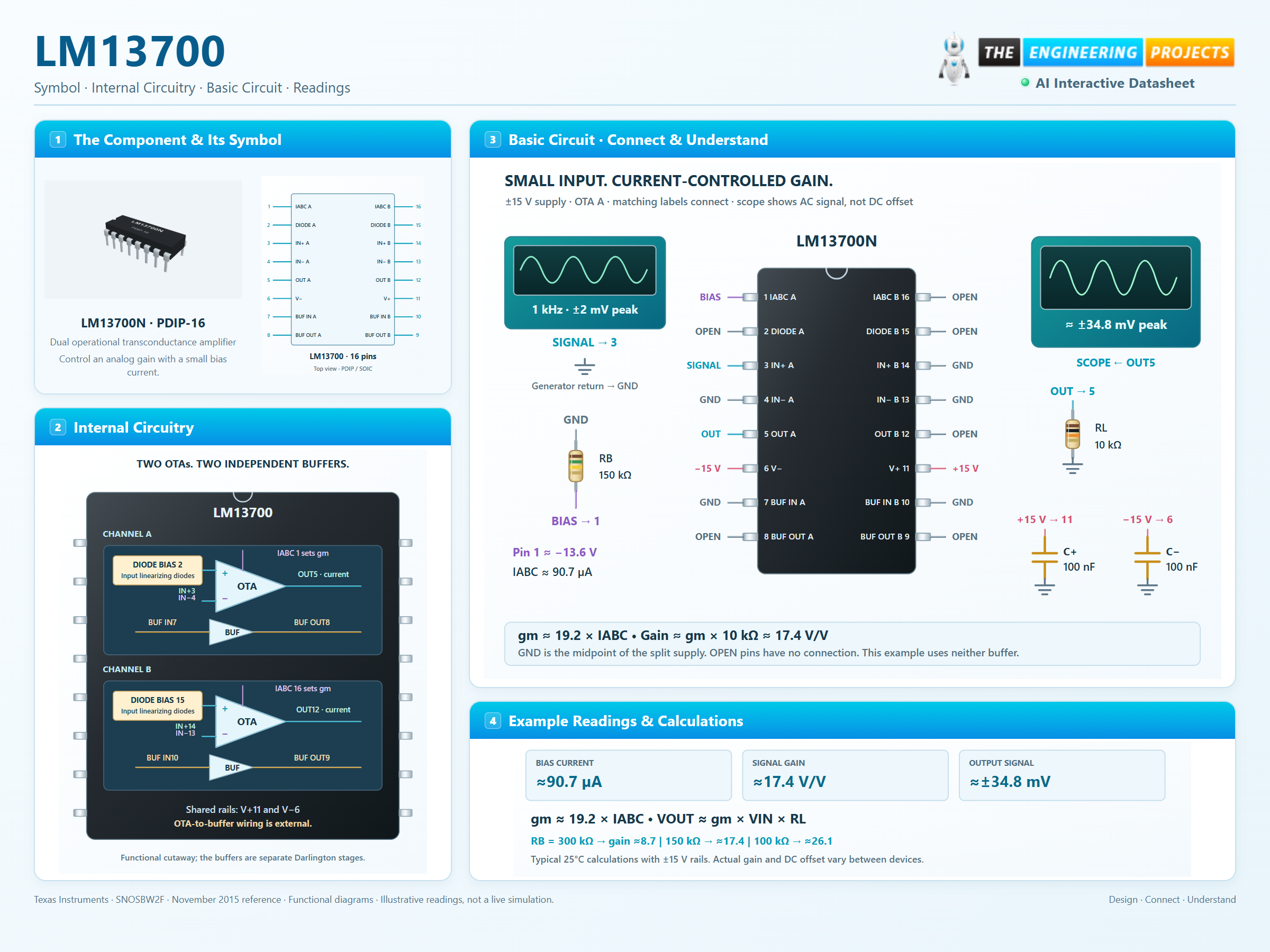
LM13700 at a glance
Follow the labeled connections and functional stages
How it works
3 stages · Explore one step at a time
Establish a bias current
A 150 kΩ resistor from GND to IABC A1 supplies roughly 90.7 µA with ±15 V rails and the typical two-junction bias voltage.
Apply a small difference
The example uses ±2 mV at IN+ A3 while IN− A4 is grounded. The input-linearizing diodes are open.
Turn current into voltage
OUT A5 drives a 10 kΩ load to GND. The nominal output signal is about ±34.8 mV, before offset and device tolerances.
Step 1 of 3
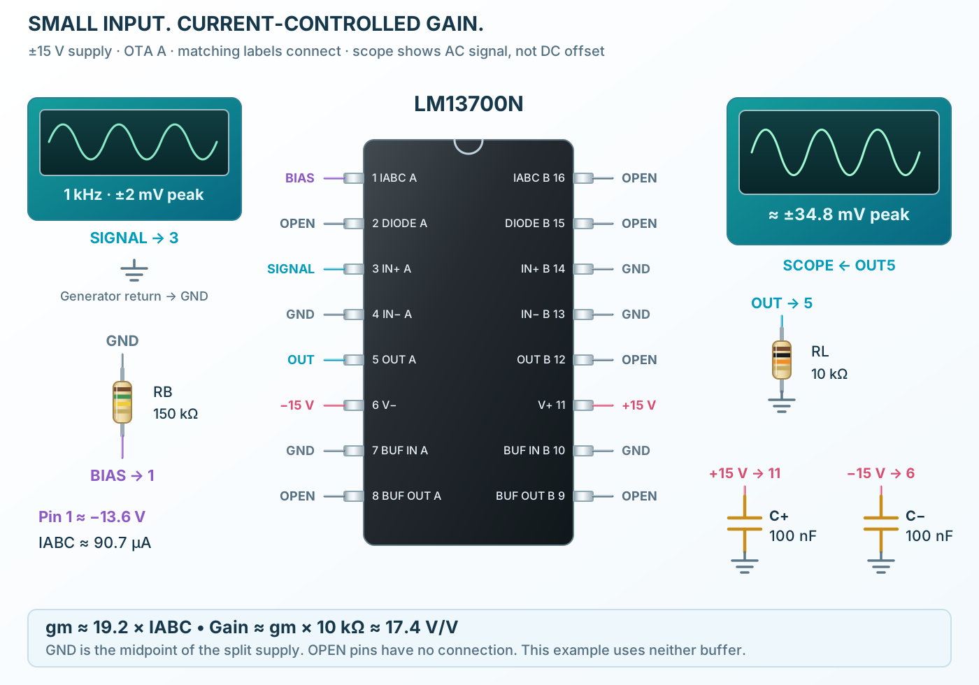
LM13700 in a circuit
A millivolt input and a resistive load reveal the OTA principle.
Connect it, step by step
Follow the component values and pin connections
Connect both rails
Connect +15 V to pin 11 and −15 V to pin 6, with local bypass to the supply midpoint.
Set and limit bias
Feed IABC A1 through 150 kΩ from GND; never short this pin directly to GND.
Compare signal amplitudes
Observe the AC output across 10 kΩ. Changing the bias resistor changes the nominal gain.
Inside LM13700
Two current-output amplifiers and two separate buffers.
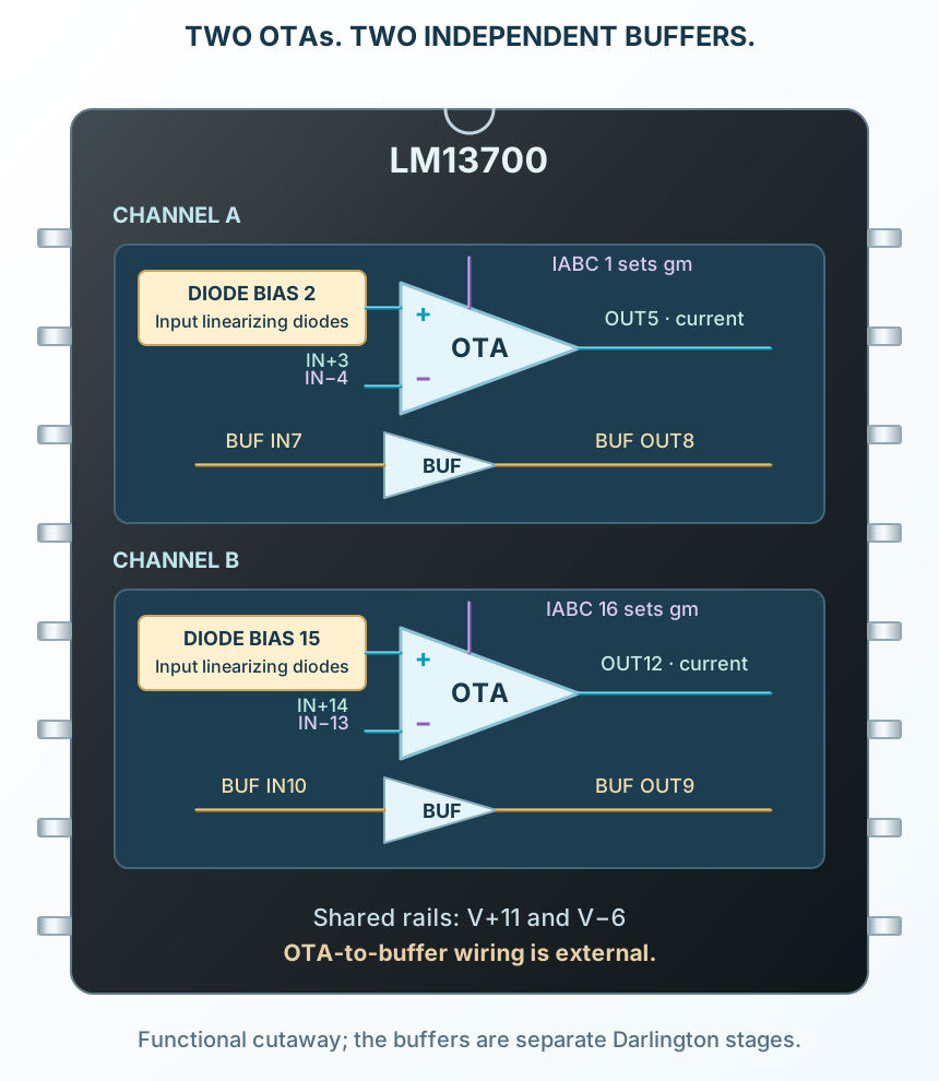
Explore the circuit
Select a stage to see its role and connections
Set gm independently
IABC A1 and IABC B16 control the two channels separately.
Linearize when needed
DIODE A2 and DIODE B15 bias input-linearizing diodes for appropriately conditioned signals.
Choose the output stage
Use the OTA current output directly, or externally connect and bias its separate buffer.
Selected packagePDIP-16LM13700N
Physical connections16 pinsPackage-specific numbering
Reference collection8 tables48 parameters & pin functions
Pin reference
Signal names, electrical functions and connection guidance
Physical pin numbers16 pins
Scroll within the table to see all columns and rows.
| Pin | Signal | Type | Function & connection |
|---|---|---|---|
| IABC A | Channel A bias current | Sets channel A transconductance through an externally supplied current.Connection guidanceFor the example, connect a 150 kΩ resistor from circuit GND to this pin. The pin sits approximately two diode drops above V−; do not drive it directly from a voltage source. Absolute maximum is 2 mA. | |
| DIODE A | Channel A diode bias | Feeds the two input-linearizing diodes.Connection guidanceLeave open in the small-signal example. Use a properly limited bias current when enabling the diodes. The diode current and input attenuation must be designed together; 2 mA is an absolute maximum. | |
| IN+ A | Channel A noninverting input | A positive differential input produces positive output current.Connection guidanceApply a 1 kHz sine wave, ±2 mV peak, centered on circuit GND. | |
| IN− A | Channel A inverting input | The OTA responds to IN+ minus IN−.Connection guidanceConnect to circuit GND in this example. Keep the differential signal small when the linearizing diodes are unused. | |
| OUT A | Channel A current output | High-impedance output supplies a current proportional to differential voltage.Connection guidanceConnect a 10 kΩ load to GND and a high-impedance scope. This is a current output, not an ordinary low-impedance voltage-amplifier output. | |
| V− | Negative supply | Negative supply for both OTAs and buffers.Connection guidanceConnect to −15 V and bypass to circuit GND with 100 nF. | |
| BUF IN A | Channel A buffer input | Independent input to the Darlington output buffer.Connection guidanceGround in this unbuffered example. It is not internally connected to OUT A pin 5. | |
| BUF OUT A | Channel A buffer output | Emitter-follower output with a two-junction level shift.Connection guidanceLeave open in this example. When used, provide a bias load toward V−. Output current and package dissipation must stay within limits; the buffer is not rail-to-rail. | |
| BUF OUT B | Channel B buffer output | Independent Darlington follower output.Connection guidanceLeave open in this example. | |
| BUF IN B | Channel B buffer input | Independent input to the second buffer.Connection guidanceConnect to circuit GND in this example. It is not internally connected to OUT B pin 12. | |
| V+ | Positive supply | Positive supply shared by both channels.Connection guidanceConnect to +15 V and bypass to circuit GND with 100 nF. | |
| OUT B | Channel B current output | Second high-impedance OTA output.Connection guidanceLeave open in this channel-A example. | |
| IN− B | Channel B inverting input | Negative differential input of the second OTA.Connection guidanceConnect to circuit GND when channel B is unused here. | |
| IN+ B | Channel B noninverting input | Positive differential input of the second OTA.Connection guidanceConnect to circuit GND when channel B is unused here. | |
| DIODE B | Channel B diode bias | Bias connection for channel B linearizing diodes.Connection guidanceLeave open in this example. | |
| IABC B | Channel B bias current | Sets the second channel transconductance independently.Connection guidanceLeave open so IABC B is zero in this example. An unused bias pin does not require a direct connection to GND. |
No pins match these filters. Try another signal name or reset the filters.
Supplies and limits
Recommended conditions and absolute ratings
Manufacturer-referenced values7 parameters
Scroll within the table to see all columns and rows.
| Parameter | Value | Conditions / notes |
|---|---|---|
| Recommended total supply | 9.5–32 V | Single-supply configuration |
| Recommended split supplies | ±4.75 to ±16 V | Symmetric dual-supply configuration |
| Example supply | +15 V / GND / −15 V | 30 V total rail span |
| Operating temperature | 0 to +70°C | Commercial grade |
| Absolute supply limit | 36 V total / ±18 V | Stress limit, not the operating target |
| Absolute IABC / diode current | 2 mA each | External current limiting is required |
| Absolute buffer output current | 20 mA | Also constrained by package dissipation |
No specifications match. Try a parameter name or a unit.
Circuit GND is the midpoint of the split supply; it is not the V− pin.
OTA characteristics
±15 V, 25°C, IABC = 500 µA unless noted
Manufacturer-referenced values8 parameters
Scroll within the table to see all columns and rows.
| Parameter | Value | Conditions / notes |
|---|---|---|
| Forward transconductance | 6.7–13 mS; 9.6 mS typical | 5.4 mS minimum over specified temperature |
| Channel gm tracking | 0.3 dB typical | Manufacturer reference conditions |
| Input offset | 0.4 mV typical; 4 mV maximum | Manufacturer specified-temperature condition |
| Input bias current | 0.4 µA typical; 5 µA maximum | 1 µA typical / 8 µA maximum over temperature |
| Input resistance | 26 kΩ typical; 10 kΩ minimum | Reference test conditions |
| Common-mode input range | ±12 V minimum; ±13.5 V typical | With ±15 V rails |
| Peak output current | 500 µA typical; 350–650 µA | IABC = 500 µA, RL = 0 |
| Supply current | 2.6 mA typical | Both channels, IABC = 500 µA |
No specifications match. Try a parameter name or a unit.
Typical transconductance and example gain are not guaranteed exact values.
Signal behavior
OTA and buffer are different stages
Manufacturer-referenced values7 parameters
Scroll within the table to see all columns and rows.
| Parameter | Value | Conditions / notes |
|---|---|---|
| Small-signal equation | IOUT ≈ gm × (VIN+ − VIN−) | Without the linearizing diodes, use a few millivolts differential |
| Typical gm at 25°C | Approximately 19.2 × IABC | IABC in amperes gives gm in siemens |
| Current-to-voltage conversion | VOUT ≈ IOUT × RL | Valid while output swing and current remain in range |
| Open-loop bandwidth | 2 MHz typical | Not a guaranteed closed-loop bandwidth for every circuit |
| Slew rate | 50 V/µs typical | Unity-gain compensated test |
| Separate buffers | Darlington emitter followers | Input must be connected externally; output has a level shift |
| Buffer load | Bias toward V− when used | Manufacturer buffer test uses 5 kΩ to V− |
No specifications match. Try a parameter name or a unit.
The LM13700 is not a pin-compatible replacement for a conventional dual voltage op amp.
Small-signal gain experiment
One OTA with an unbuffered resistive output
Manufacturer-referenced values8 parameters
Scroll within the table to see all columns and rows.
| Parameter | Value | Conditions / notes |
|---|---|---|
| V+11 / V−6 | +15 V / −15 V | 100 nF bypass from each rail to GND |
| IABC A1 | 150 kΩ to GND | Approximately 90.7 µA at the assumed bias voltage |
| IN+ A3 / IN− A4 | ±2 mV sine / GND | 1 kHz, zero DC offset |
| OUT A5 | 10 kΩ to GND plus high-impedance scope | Scope input capacitance affects high-frequency response |
| DIODE A2 and B15 | Open | Linearizing diodes unused in this experiment |
| BUF IN A7 and B10 | GND | BUF OUT A8 and B9 left open |
| Unused channel B | IN−13 and IN+14 to GND | IABC B16 and OUT B12 open |
| All source returns | Circuit GND | The split-supply midpoint, not −15 V |
No specifications match. Try a parameter name or a unit.
This is an explanatory circuit, not a running simulation. Offset and bias currents may add a DC output offset.
Gain calculation
Nominal 25°C example
Manufacturer-referenced values7 parameters
Scroll within the table to see all columns and rows.
| Parameter | Value | Conditions / notes |
|---|---|---|
| Bias pin estimate | V− + 2 VBE ≈ −13.6 V | Assume VBE ≈ 0.7 V |
| Bias current | 13.6 V / 150 kΩ ≈ 90.7 µA | Resistor goes from GND to IABC A1 |
| Transconductance | 19.2 × 90.7 µA ≈ 1.74 mS | Typical small-signal approximation |
| Voltage gain | 1.74 mS × 10 kΩ ≈ 17.4 V/V | About 24.8 dB |
| Signal output | 2 mV peak × 17.4 ≈ 34.8 mV peak | Excludes DC offset and tolerances |
| Use 300 kΩ instead | Approximately 8.7 V/V | Lower bias reduces gain |
| Use 100 kΩ instead | Approximately 26.1 V/V | Higher bias increases gain |
No specifications match. Try a parameter name or a unit.
Changing temperature, resistor tolerance, junction voltage or the actual gm changes these results.
Using the linearizing diodes
Advanced input conditioning
Manufacturer-referenced values6 parameters
Scroll within the table to see all columns and rows.
| Parameter | Value | Conditions / notes |
|---|---|---|
| Purpose | Reduce transfer nonlinearity | The diodes must be biased with current |
| Diode current requirement | ID greater than twice input signal current | Use the manufacturer circuit and input attenuation |
| Manufacturer VCA example | About 1 mA diode bias | 13 kΩ from +15 V, approximate 0.7 V diode node |
| Input amplitude | Attenuate before the OTA | A large differential voltage clips or distorts without suitable conditioning |
| Control-voltage conversion | Resistor feeds IABC from a control voltage | Include the V− + 2 VBE bias-pin offset |
| Buffer wiring | OUT5 to BUF IN7 only when intended | This connection is external, not inside the IC |
No specifications match. Try a parameter name or a unit.
The simple illustrated circuit deliberately leaves the diodes and buffers unused to isolate the gm principle.
Packages and ordering
LM13700N · PDIP-16
Manufacturer-referenced values5 parameters
Scroll within the table to see all columns and rows.
| Parameter | Value | Conditions / notes |
|---|---|---|
| SOIC-16 | LM13700M/NOPB; LM13700MX/NOPB | Listed in TI ordering appendix dated 10 November 2025 |
| PDIP-16 | LM13700N | Historical package documented in the datasheet; not listed in that current appendix |
| Pin map | Same 16 physical functions | Top view, pin 1 at the notch end |
| Body / pitch | PDIP: 19.304 × 6.35 mm / 2.54 mm | SOIC: 9.90 × 3.91 mm / 1.27 mm |
| Footprint provenance | Original TEP editable land patterns | Verify the exact mechanical drawing and assembly process |
No specifications match. Try a parameter name or a unit.
Legacy package visualization is not a claim of current availability.
No matching rowsTry a pin name, parameter, unit or test condition, or reset the filters.
Voltage-controlled audio
Convert a control signal to bias current for volume or modulation circuits.
Manufacturer application guideTunable filters
Use the bias-controlled transconductance in integrators and filter structures.
Manufacturer application guideOscillators and shaping
Build current-controlled analog functions with suitable surrounding circuitry.
Manufacturer application guideTake it into ProTech
Find LM13700 in the Components Library to place its schematic symbol and connect its pins.
Reference page · circuit simulation model not yet availableOpen ProTech