Real View
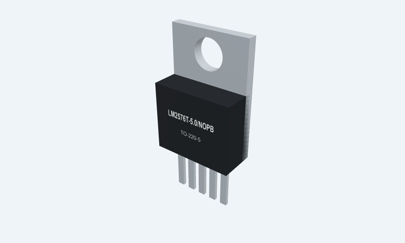
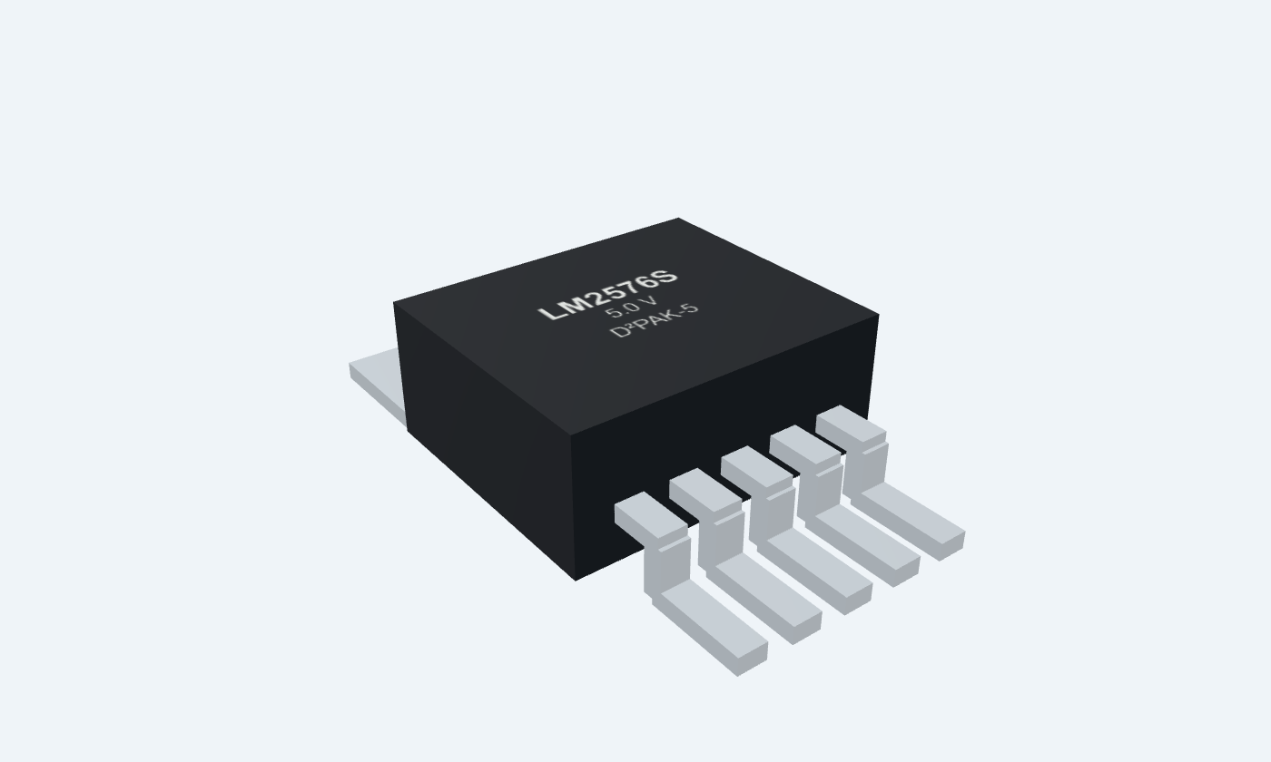
Switch, store and smooth: a lower DC voltage with less wasted heat.
LM2576 is a five-pin step-down switching regulator. This reference follows TI’s fixed 5 V versions in TO-220 and D²PAK packages; 3.3 V, 12 V, 15 V and adjustable versions are separate ordering options. An internal 52 kHz controller switches the input into an external inductor. A Schottky catch diode carries current while the switch is off, and the output capacitor smooths the filtered DC rail. The regulator can support up to 3 A with suitable external parts and cooling. Pin 2 is the switching node, pin 4 senses the filtered output, and pin 3 and the metal tab are ground.
Select a pin to explore its connection
Click a lead or use the arrow keys. Front view · leads down · pin 3 and tab are GND
Supplies the internal power switch, control circuit and bias current.
Connect the positive DC supply and a short, local input bypass to ground.
The 5 V version is specified with 8–40 V input under its stated load conditions; 45 V is an absolute maximum, not an operating target.
Pulsed output of the internal high-side switch. This node drives the external inductor.
Connect to the inductor input and Schottky cathode. The diode anode returns to GND.
This is not the filtered 5 V rail. Keep switch-node copper compact and away from feedback wiring.
Common return for the controller and power stage. The exposed metal tab is also ground.
Connect to the input-capacitor return, catch-diode anode and output-capacitor return with short power paths.
On the SMD footprint, pin 3 and the thermal-pad sections have the same electrical pad number.
Senses the filtered output and closes the regulation loop. The fixed 5 V device includes its feedback divider internally.
For the fixed 5 V example, connect directly to the output after the inductor, near COUT.
The adjustable variant instead needs an external divider referenced to approximately 1.23 V. Do not mix the two circuits.
Low enables switching; high shuts the regulator down.
Connect to ground for an always-on converter.
Logic ON is guaranteed at 0.8 V or below and OFF at 2.4 V or above over the specified temperature range. The typical switching threshold is approximately 1.4 V.
Use an inductor, catch diode and suitable input/output capacitors. The filtered output—not the switch node—feeds the load and feedback pin.
LM2576T-5.0/NOPB · TO-220-5
| Property | Details |
|---|---|
| Manufacturer | Texas Instruments |
| Part number | LM2576T-5.0/NOPB |
| Package | TO-220-5 |
| Connections | 5 pins |
| Mounting | Through-hole |
| Lead pitch | 1.70 mm |
| Package code | KC |
| Thermal reference | Grounded tab; thermal performance depends on board copper and cooling |
Output and voltage class are ordering options
Scroll sideways to see all columns.
| Parameter | Value | Conditions / notes |
|---|---|---|
| Selected fixed output | 5 V | LM2576T-5.0/NOPB and LM2576S-5.0/NOPB |
| Other fixed outputs | 3.3 V / 12 V / 15 V | Choose the matching suffix; changing a resistor does not reprogram a fixed version |
| Adjustable option | 1.23–37 V nominal range | ADJ version uses an external divider; input headroom is still needed |
| HV version | 60 V recommended supply ceiling | A separately ordered device; the selected non-HV parts remain limited to 40 V |
| Straight TO-220 leads | KC0005A | Do not substitute the footprint for LF02/LF03 formed-lead orderables |
| Grounded tab | Pin 3 electrical node | A heatsink or exposed pad can be electrically live at ground potential |
No specifications match. Try a parameter name or a unit.
The package switch changes the physical package, not the regulator family or output-voltage suffix.
Fixed 5 V option · TI SNVS107G
Scroll sideways to see all columns.
| Parameter | Value | Conditions / notes |
|---|---|---|
| Nominal output | 5 V | LM2576T-5.0 / LM2576S-5.0 |
| Specified input for 5 V regulation | 8–40 V | 0.5–3 A output load |
| Output at 25°C | 4.8–5.2 V | VIN = 8–40 V; ILOAD = 0.5–3 A |
| Output over temperature | 4.75–5.25 V | Same input/load range; TJ = −40–125°C |
| Output current | Up to 3 A | Inductor, diode, capacitors, layout and cooling must support the load |
| Non-HV supply ceiling | 40 V maximum | The fixed 5 V regulation table uses 8–40 V input |
No specifications match. Try a parameter name or a unit.
Output accuracy includes the manufacturer’s stated conditions; do not use a headline current rating without thermal review.
Typical values retain their test conditions
Scroll sideways to see all columns.
| Parameter | Value | Conditions / notes |
|---|---|---|
| Oscillator | 52 kHz typical | 47–58 kHz at 25°C; 42–63 kHz over temperature |
| Switch saturation | 1.4 V typical | 3 A switch current; 1.8 V maximum at 25°C |
| Peak switch-current limit | 5.8 A typical | Protection threshold; not a continuous output rating |
| Shutdown threshold | 1.4 V typical | High = OFF; low = ON |
| Guaranteed enable / shutdown | ≤ 0.8 V / ≥ 2.4 V | Logic thresholds over specified temperature range |
| Standby supply current | 50 µA typical | ON/OFF = 5 V; 200 µA maximum under the stated test conditions |
No specifications match. Try a parameter name or a unit.
The internal switch and diode have losses; the actual duty ratio is above the ideal VOUT/VIN estimate.
Nominal 1 A load · illustrative component selection
Scroll sideways to see all columns.
| Parameter | Value | Conditions / notes |
|---|---|---|
| Input / output | 12 V DC / 5 V DC | Fixed-output device; pin 4 connected directly to filtered output |
| Inductor L1 | 100 µH | Choose saturation/current ratings for load, ripple and current-limit behavior |
| Catch diode D1 | MBR360 · 3 A, 60 V Schottky | Cathode to pin 2; anode to GND; suitable for this 12 V illustration |
| Input CIN | 100 µF, 50 V | Low-ESR aluminum; check RMS ripple rating |
| Output COUT | 1000 µF, 25 V | Low-ESR aluminum; check TI ESR/stability guidance |
| Load | 5 Ω · at least 10 W | 1 A nominal; resistor dissipates 5 W |
No specifications match. Try a parameter name or a unit.
The inductor, diode and nominal capacitances follow TI’s fixed-output application. Input voltage and load here are a 12 V, 1 A teaching example. Validate startup, ripple, stability and thermal margins for the actual parts and conditions.
Ideal continuous-conduction estimates
Scroll sideways to see all columns.
| Parameter | Value | Conditions / notes |
|---|---|---|
| Duty ratio | D ≈ 5 / 12 = 41.7% | Neglects switch and diode voltage drops |
| Switch period | 19.23 µs | 1 / 52 kHz |
| ON time | 8.01 µs | D / f |
| Inductor ripple | Approximately 0.561 A peak-to-peak | (12 − 5) × D / (100 µH × 52 kHz) |
| Peak current at 1 A average | Approximately 1.280 A | ILOAD + ΔIL/2 in ideal steady state |
| Output power | 5 W | 5 V × 1 A |
No specifications match. Try a parameter name or a unit.
This calculation is a teaching aid. It is not a full SPICE simulation or a guarantee of measured ripple.
Short switching loops · correct thermal-pad mapping
Scroll sideways to see all columns.
| Parameter | Value | Conditions / notes |
|---|---|---|
| Input loop | CIN → VIN → internal switch → diode → CIN return | Place CIN and diode close to the IC |
| Switch node | Pin 2 to L1 and diode cathode | Keep copper compact and away from feedback |
| Feedback | Pin 4 to COUT positive / output | Use a quiet sense route, away from switch node |
| Ground / tab | Pin 3 plus exposed metal tab | Ground plane and cooling path |
| TO-220 footprint | KC straight-lead pattern | 1.70 mm pitch; five holes in one row |
| D²PAK footprint | KTT five leads plus stepped thermal land | All pad-3 sections are GND |
No specifications match. Try a parameter name or a unit.
The downloads contain electrical pads and outlines. Check the chosen lead form, solder process and heatsinking before manufacture.
Separate operating conditions from stress ratings
Scroll sideways to see all columns.
| Parameter | Value | Conditions / notes |
|---|---|---|
| Operating junction temperature | −40 to +125°C | Recommended range |
| Supply absolute maximum | 45 V | Stress rating; recommended VIN maximum is 40 V |
| Junction absolute maximum | 150°C | Not a normal operating target |
| Storage temperature | −65 to +150°C | Unpowered |
| TO-220 RθJA | 32.4°C/W | JEDEC four-layer board; real board and heatsinking change this value |
| TO-263 RθJA | 42.6°C/W | JEDEC four-layer board; depends strongly on copper and cooling |
No specifications match. Try a parameter name or a unit.
Thermal shutdown and current limiting provide protection; they do not replace a suitable board and cooling design.
Select a pin for its function, connection guidance and electrical notes.
Follow the labeled connections and functional stages
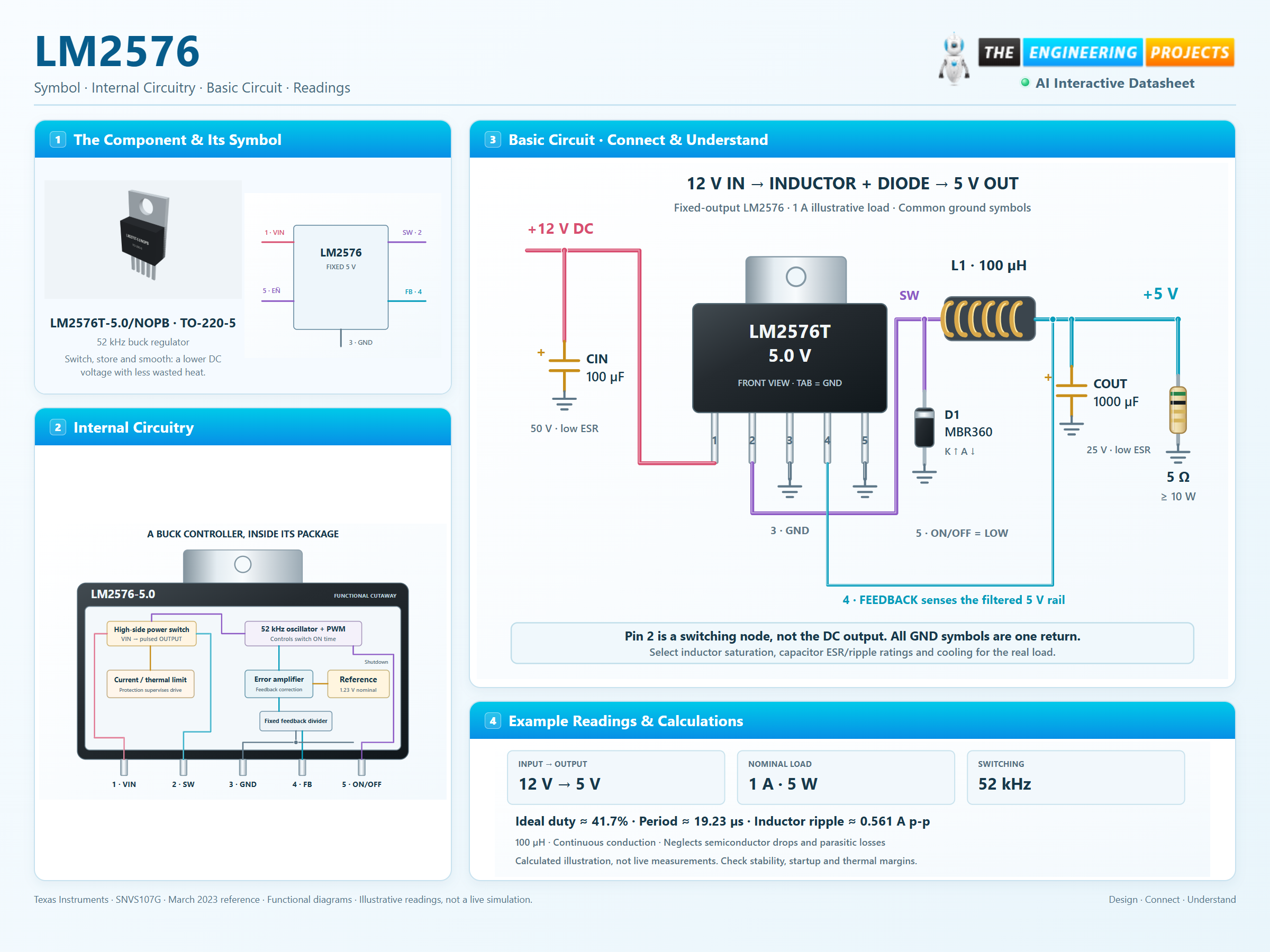
3 stages · Explore one step at a time
The internal transistor connects VIN to pin 2. Inductor current rises while energy flows toward the load.
The catch diode conducts from ground into the switch node. Inductor current continues toward the load and falls gradually.
Feedback senses the filtered output. The controller adjusts pulse width, while current limiting and thermal shutdown handle abnormal conditions.
Five physical leads, an energy-storage inductor and a catch diode.
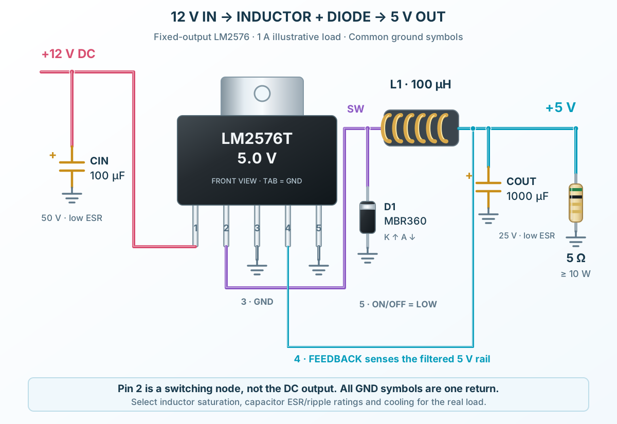
Follow the component values and pin connections
Feed pin 1 from 12 V and keep the input capacitor close to the switching-current loop.
Pin 2 feeds L1. D1 provides the OFF-state current path; its cathode is at the switch node.
Connect pin 4 after L1. Ground pin 5 for continuous operation and pin 3/tab for the common return.
Switching control drawn inside the five-pin package.
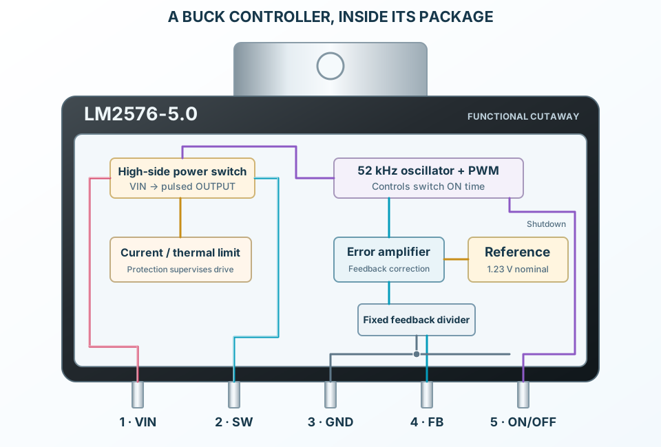
Select a stage to see its role and connections
An internal divider scales the fixed 5 V output sensed at pin 4 for comparison with the reference.
The error signal and oscillator control the power-switch pulse width.
The switch feeds pin 2. Current and temperature protections supervise operation.
Signal names, electrical functions and connection guidance
Scroll within the table to see all columns and rows.
| Pin | Signal | Type | Function & connection |
|---|---|---|---|
| VIN | Supply input | Supplies the internal power switch, control circuit and bias current.Connection guidanceConnect the positive DC supply and a short, local input bypass to ground. The 5 V version is specified with 8–40 V input under its stated load conditions; 45 V is an absolute maximum, not an operating target. | |
| SW | Switch node | Pulsed output of the internal high-side switch. This node drives the external inductor.Connection guidanceConnect to the inductor input and Schottky cathode. The diode anode returns to GND. This is not the filtered 5 V rail. Keep switch-node copper compact and away from feedback wiring. | |
| GND | Ground and metal tab | Common return for the controller and power stage. The exposed metal tab is also ground.Connection guidanceConnect to the input-capacitor return, catch-diode anode and output-capacitor return with short power paths. On the SMD footprint, pin 3 and the thermal-pad sections have the same electrical pad number. | |
| FB | Output sense | Senses the filtered output and closes the regulation loop. The fixed 5 V device includes its feedback divider internally.Connection guidanceFor the fixed 5 V example, connect directly to the output after the inductor, near COUT. The adjustable variant instead needs an external divider referenced to approximately 1.23 V. Do not mix the two circuits. | |
| ON/OFF | Shutdown input | Low enables switching; high shuts the regulator down.Connection guidanceConnect to ground for an always-on converter. Logic ON is guaranteed at 0.8 V or below and OFF at 2.4 V or above over the specified temperature range. The typical switching threshold is approximately 1.4 V. |
No pins match these filters. Try another signal name or reset the filters.
Output and voltage class are ordering options
Scroll within the table to see all columns and rows.
| Parameter | Value | Conditions / notes |
|---|---|---|
| Selected fixed output | 5 V | LM2576T-5.0/NOPB and LM2576S-5.0/NOPB |
| Other fixed outputs | 3.3 V / 12 V / 15 V | Choose the matching suffix; changing a resistor does not reprogram a fixed version |
| Adjustable option | 1.23–37 V nominal range | ADJ version uses an external divider; input headroom is still needed |
| HV version | 60 V recommended supply ceiling | A separately ordered device; the selected non-HV parts remain limited to 40 V |
| Straight TO-220 leads | KC0005A | Do not substitute the footprint for LF02/LF03 formed-lead orderables |
| Grounded tab | Pin 3 electrical node | A heatsink or exposed pad can be electrically live at ground potential |
No specifications match. Try a parameter name or a unit.
The package switch changes the physical package, not the regulator family or output-voltage suffix.
Fixed 5 V option · TI SNVS107G
Scroll within the table to see all columns and rows.
| Parameter | Value | Conditions / notes |
|---|---|---|
| Nominal output | 5 V | LM2576T-5.0 / LM2576S-5.0 |
| Specified input for 5 V regulation | 8–40 V | 0.5–3 A output load |
| Output at 25°C | 4.8–5.2 V | VIN = 8–40 V; ILOAD = 0.5–3 A |
| Output over temperature | 4.75–5.25 V | Same input/load range; TJ = −40–125°C |
| Output current | Up to 3 A | Inductor, diode, capacitors, layout and cooling must support the load |
| Non-HV supply ceiling | 40 V maximum | The fixed 5 V regulation table uses 8–40 V input |
No specifications match. Try a parameter name or a unit.
Output accuracy includes the manufacturer’s stated conditions; do not use a headline current rating without thermal review.
Typical values retain their test conditions
Scroll within the table to see all columns and rows.
| Parameter | Value | Conditions / notes |
|---|---|---|
| Oscillator | 52 kHz typical | 47–58 kHz at 25°C; 42–63 kHz over temperature |
| Switch saturation | 1.4 V typical | 3 A switch current; 1.8 V maximum at 25°C |
| Peak switch-current limit | 5.8 A typical | Protection threshold; not a continuous output rating |
| Shutdown threshold | 1.4 V typical | High = OFF; low = ON |
| Guaranteed enable / shutdown | ≤ 0.8 V / ≥ 2.4 V | Logic thresholds over specified temperature range |
| Standby supply current | 50 µA typical | ON/OFF = 5 V; 200 µA maximum under the stated test conditions |
No specifications match. Try a parameter name or a unit.
The internal switch and diode have losses; the actual duty ratio is above the ideal VOUT/VIN estimate.
Nominal 1 A load · illustrative component selection
Scroll within the table to see all columns and rows.
| Parameter | Value | Conditions / notes |
|---|---|---|
| Input / output | 12 V DC / 5 V DC | Fixed-output device; pin 4 connected directly to filtered output |
| Inductor L1 | 100 µH | Choose saturation/current ratings for load, ripple and current-limit behavior |
| Catch diode D1 | MBR360 · 3 A, 60 V Schottky | Cathode to pin 2; anode to GND; suitable for this 12 V illustration |
| Input CIN | 100 µF, 50 V | Low-ESR aluminum; check RMS ripple rating |
| Output COUT | 1000 µF, 25 V | Low-ESR aluminum; check TI ESR/stability guidance |
| Load | 5 Ω · at least 10 W | 1 A nominal; resistor dissipates 5 W |
No specifications match. Try a parameter name or a unit.
The inductor, diode and nominal capacitances follow TI’s fixed-output application. Input voltage and load here are a 12 V, 1 A teaching example. Validate startup, ripple, stability and thermal margins for the actual parts and conditions.
Ideal continuous-conduction estimates
Scroll within the table to see all columns and rows.
| Parameter | Value | Conditions / notes |
|---|---|---|
| Duty ratio | D ≈ 5 / 12 = 41.7% | Neglects switch and diode voltage drops |
| Switch period | 19.23 µs | 1 / 52 kHz |
| ON time | 8.01 µs | D / f |
| Inductor ripple | Approximately 0.561 A peak-to-peak | (12 − 5) × D / (100 µH × 52 kHz) |
| Peak current at 1 A average | Approximately 1.280 A | ILOAD + ΔIL/2 in ideal steady state |
| Output power | 5 W | 5 V × 1 A |
No specifications match. Try a parameter name or a unit.
This calculation is a teaching aid. It is not a full SPICE simulation or a guarantee of measured ripple.
Short switching loops · correct thermal-pad mapping
Scroll within the table to see all columns and rows.
| Parameter | Value | Conditions / notes |
|---|---|---|
| Input loop | CIN → VIN → internal switch → diode → CIN return | Place CIN and diode close to the IC |
| Switch node | Pin 2 to L1 and diode cathode | Keep copper compact and away from feedback |
| Feedback | Pin 4 to COUT positive / output | Use a quiet sense route, away from switch node |
| Ground / tab | Pin 3 plus exposed metal tab | Ground plane and cooling path |
| TO-220 footprint | KC straight-lead pattern | 1.70 mm pitch; five holes in one row |
| D²PAK footprint | KTT five leads plus stepped thermal land | All pad-3 sections are GND |
No specifications match. Try a parameter name or a unit.
The downloads contain electrical pads and outlines. Check the chosen lead form, solder process and heatsinking before manufacture.
Separate operating conditions from stress ratings
Scroll within the table to see all columns and rows.
| Parameter | Value | Conditions / notes |
|---|---|---|
| Operating junction temperature | −40 to +125°C | Recommended range |
| Supply absolute maximum | 45 V | Stress rating; recommended VIN maximum is 40 V |
| Junction absolute maximum | 150°C | Not a normal operating target |
| Storage temperature | −65 to +150°C | Unpowered |
| TO-220 RθJA | 32.4°C/W | JEDEC four-layer board; real board and heatsinking change this value |
| TO-263 RθJA | 42.6°C/W | JEDEC four-layer board; depends strongly on copper and cooling |
No specifications match. Try a parameter name or a unit.
Thermal shutdown and current limiting provide protection; they do not replace a suitable board and cooling design.
No matching rowsTry a pin name, parameter, unit or test condition, or reset the filters.
Create a lower-voltage rail from a higher DC supply when the input range, noise and load requirements suit the design.
Manufacturer application guideExplore the difference between switching-node pulses, inductor current and the filtered output.
Manufacturer application guidePlace a buck stage near the load with short high-current loops and carefully routed feedback.
Manufacturer application guideFind LM2576 in the Components Library to place its schematic symbol and connect its pins.
Reference page · circuit simulation model not yet availableOpen ProTech