Real View
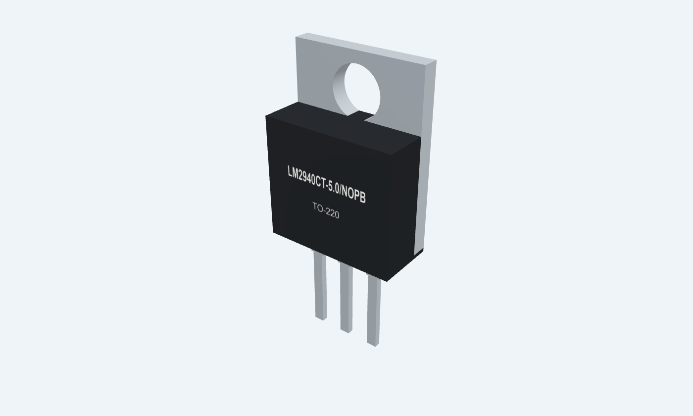
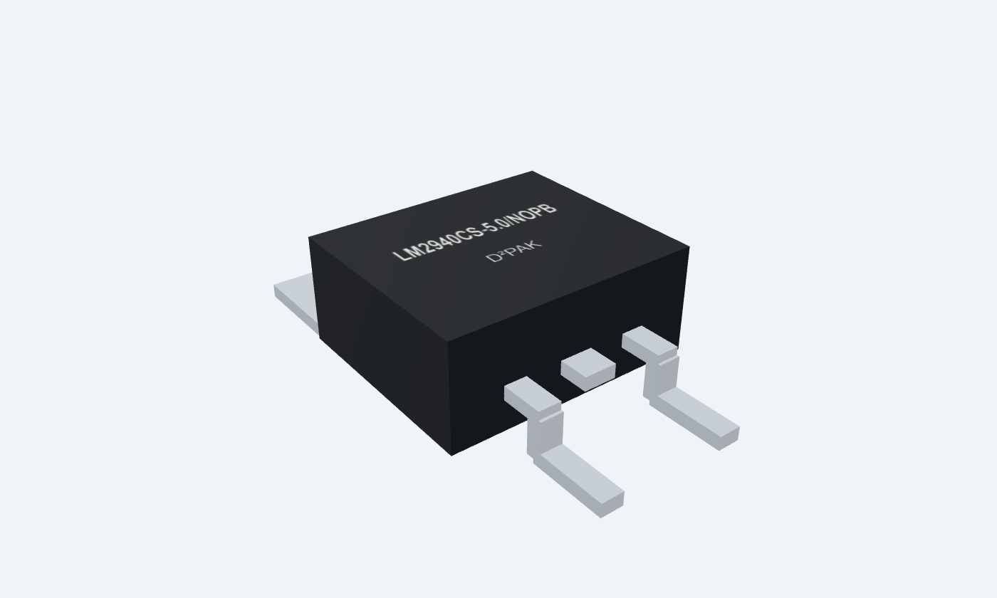
A regulated +5 V rail with three electrical connections.
LM2940T-5 is a three-terminal regulator that produces a nominal +5 V output from a higher positive DC source. This page selects LM2940CT-5.0/NOPB in TO-220 and LM2940CS-5.0/NOPB in its surface-mount package. The internal reference, feedback amplifier and series pass device form the voltage-control loop. The LM2940C uses a low-dropout pass stage, but its output capacitor is part of the stability design. Use at least 22 µF effective capacitance with ESR in the manufacturer’s permitted range across load and temperature. An arbitrary low-ESR ceramic substitution can oscillate. The illustrated +7.5 V-to-+5 V supply drives a 50 Ω load at approximately 100 mA. The load dissipates 0.50 W and the pass stage loses about 0.25 W before ground-current losses. All package views follow the selected part; the example is a DC circuit reference, not a live simulation.
Select a pin to explore its connection
Click a lead or use the arrow keys. Front view · marking toward you · leads down
Feeds the series pass stage.
Apply +7.5 V and fit 0.47 µF local input bypass.
Metal tab is electrically GND.
Join supply return, load and capacitor returns.
Supplies nominal +5 V within regulation and thermal limits.
Connect the load and 22 µF to ground.
Output capacitance and ESR are required for stability.
A regulated +5 V rail with three electrical connections.
LM2940CT-5.0/NOPB · TO-220
| Property | Details |
|---|---|
| Manufacturer | Texas Instruments |
| Part number | LM2940CT-5.0/NOPB |
| Package | TO-220 |
| Connections | 3 pins |
| Mounting | Through-hole |
| Lead pitch | 2.54 mm |
| Package code | V |
| Thermal reference | Check the manufacturer package and mounting conditions |
Front view, marking toward you
Scroll sideways to see all columns.
| Parameter | Value | Conditions / notes |
|---|---|---|
| 1 · INPUT | Feeds the series pass stage. | Apply +7.5 V and fit 0.47 µF local input bypass. |
| 2 · GND | Metal tab is electrically GND. | Join supply return, load and capacitor returns. |
| 3 · OUTPUT | Supplies nominal +5 V within regulation and thermal limits. | Connect the load and 22 µF to ground. |
No specifications match. Try a parameter name or a unit.
The exposed tab duplicates pin 2. Verify polarity before applying power.
LM2940CT-5.0/NOPB / LM2940CS-5.0/NOPB
Scroll sideways to see all columns.
| Parameter | Value | Conditions / notes |
|---|---|---|
| Output at 25°C | 4.85–5.15 V | 5 mA–1 A; specified input range |
| Output across stated range | 4.75–5.25 V | 5 mA–1 A; selected C grade |
| Input for 5 V regulation specification | 6.25–26 V | More specific than family headline |
| Load regulation | 35 mV typical; 50 mV max | 50 mA–1 A; LM2940C |
| Ground current at 1 A | 30 mA typical; 45 mA max at 25°C | VIN = VOUT + 5 V; 60 mA max over temperature |
| Output noise | 150 µV RMS typical | 10 Hz–100 kHz; 5 mA |
| Ripple rejection | 72 dB typical; 60 dB min | 120 Hz; 100 mA; LM2940C |
No specifications match. Try a parameter name or a unit.
Read the exact test conditions. Typical values are not guaranteed limits.
Local components near the regulator
Scroll sideways to see all columns.
| Parameter | Value | Conditions / notes |
|---|---|---|
| Input bypass | 0.47 µF | IN 1 to GND 2 |
| Output capacitor | 22 µF | OUT 3 to GND 2 |
| Capacitor selection | At least 22 µF, ESR 0.1–1 Ω | Maintain effective capacitance and ESR across temperature |
| Tab / thermal pad | GND | Electrically connected to pin 2 |
| Dropout | 0.5 V typical; 0.8 V max at 1 A, 25°C; 1 V max over temperature | Not an unconditional fixed input margin |
No specifications match. Try a parameter name or a unit.
Short return paths and correct capacitor characteristics matter.
100 mA nominal DC load
Scroll sideways to see all columns.
| Parameter | Value | Conditions / notes |
|---|---|---|
| Input / output | +7.5 V / +5 V | DC source with sufficient headroom |
| Load | 50 Ω | Dissipation 0.50 W; choose adequate derating |
| Current | 5 V / 50 Ω = 0.10 A | Nominal calculation |
| Pass loss | 0.25 W | (7.5 − 5) V × 0.10 A |
| Total regulator loss | Pass loss + |VIN| × IGND | Ground current also produces heat |
| Cooling | TJ ≈ TA + PD × θJA | Use thermal resistance for actual mounting |
No specifications match. Try a parameter name or a unit.
Respect resistor rating, input ripple and regulator dissipation.
LM2940CT-5.0/NOPB · TO-220
Scroll sideways to see all columns.
| Parameter | Value | Conditions / notes |
|---|---|---|
| Lead pitch | 2.54 mm | Through-hole |
| Selected temperature grade | 0–125°C | LM2940C; other LM2940-N grades differ |
| Input stress limit | 26 V operating maximum; see transient limits | Do not use stress limits as a normal design target |
| Storage | −65 to +150°C | Unpowered |
| Package mapping | 1 INPUT; 2 GND; 3 OUTPUT | Thermal pad duplicates pin 2 |
No specifications match. Try a parameter name or a unit.
Verify the manufacturer package drawing and footprint before PCB manufacture.
Select a pin for its function, connection guidance and electrical notes.
Follow the labeled connections and functional stages
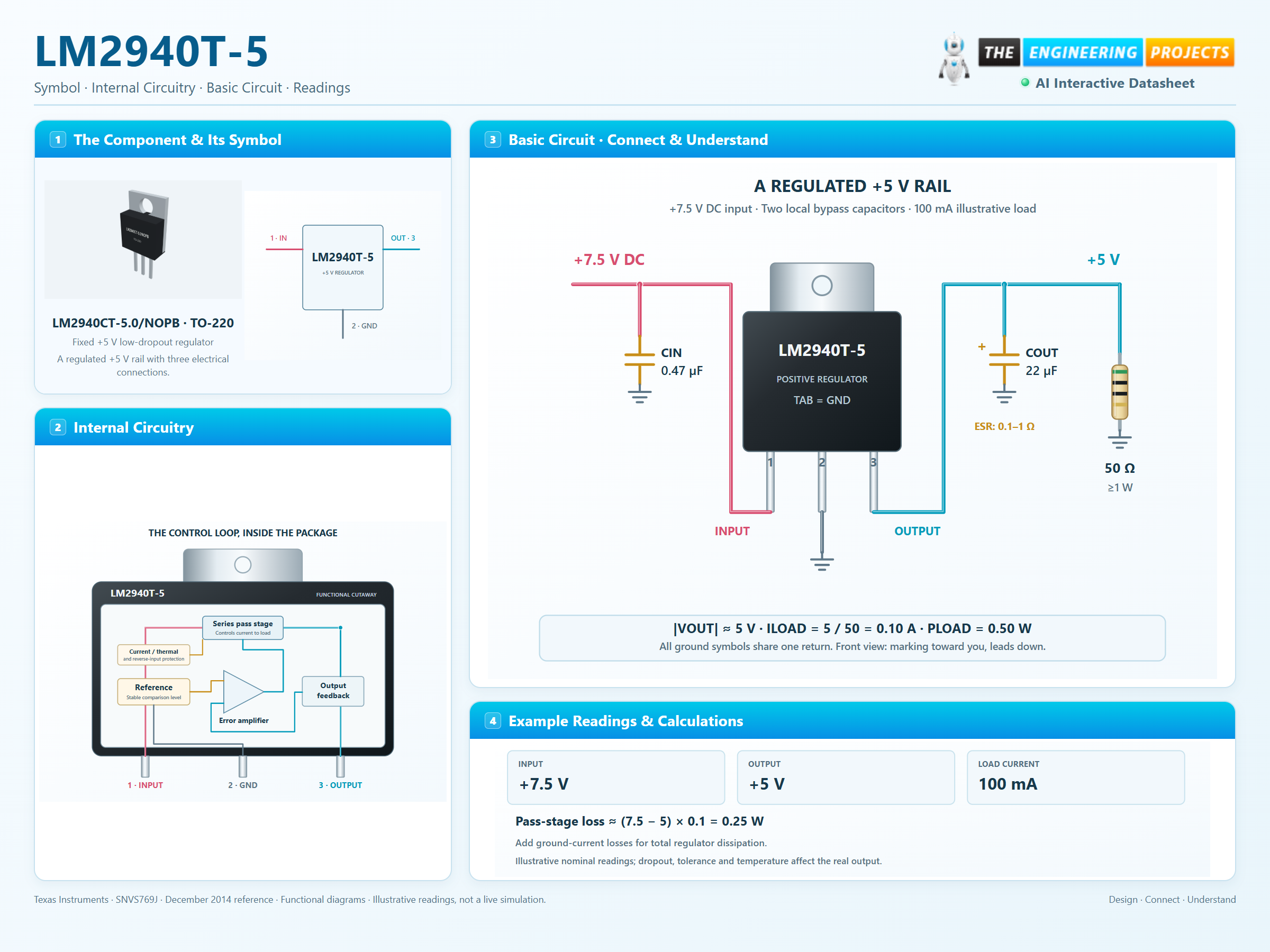
3 stages · Explore one step at a time
The internal reference establishes the desired output level.
The feedback amplifier controls the series pass stage.
Voltage drop and ground current generate heat that must leave the package.
Realistic package, local capacitors and a rated load.
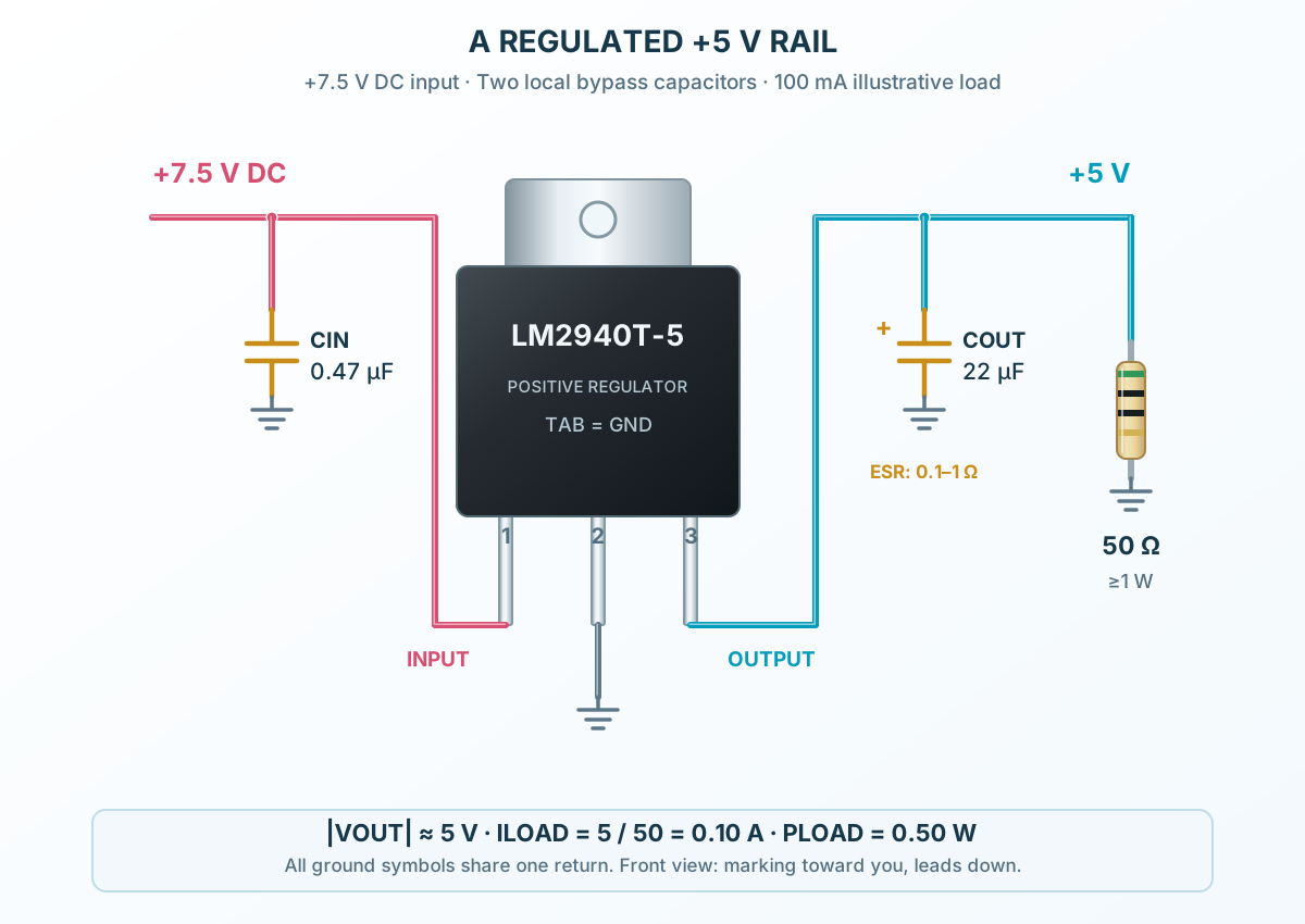
Follow the component values and pin connections
Apply +7.5 V to pin 1.
Fit at least 22 µF with suitable ESR at the output.
Connect 50 Ω from output to ground with adequate power rating.
Compact reference, feedback, pass stage and protection.
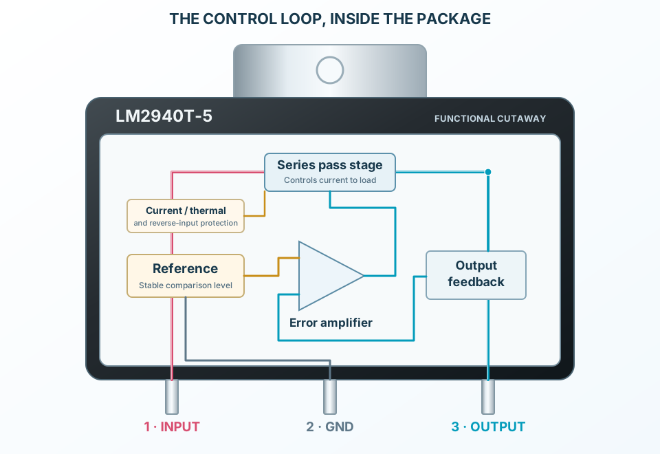
Select a stage to see its role and connections
Compare output feedback with the reference.
Adjust the pass stage.
Limit abnormal current and temperature.
Signal names, electrical functions and connection guidance
Scroll within the table to see all columns and rows.
| Pin | Signal | Type | Function & connection |
|---|---|---|---|
| INPUT | Supply input | Feeds the series pass stage.Connection guidanceApply +7.5 V and fit 0.47 µF local input bypass. | |
| GND | Reference, return and tab | Metal tab is electrically GND.Connection guidanceJoin supply return, load and capacitor returns. | |
| OUTPUT | Regulated output | Supplies nominal +5 V within regulation and thermal limits.Connection guidanceConnect the load and 22 µF to ground. Output capacitance and ESR are required for stability. |
No pins match these filters. Try another signal name or reset the filters.
Front view, marking toward you
Scroll within the table to see all columns and rows.
| Parameter | Value | Conditions / notes |
|---|---|---|
| 1 · INPUT | Feeds the series pass stage. | Apply +7.5 V and fit 0.47 µF local input bypass. |
| 2 · GND | Metal tab is electrically GND. | Join supply return, load and capacitor returns. |
| 3 · OUTPUT | Supplies nominal +5 V within regulation and thermal limits. | Connect the load and 22 µF to ground. |
No specifications match. Try a parameter name or a unit.
The exposed tab duplicates pin 2. Verify polarity before applying power.
LM2940CT-5.0/NOPB / LM2940CS-5.0/NOPB
Scroll within the table to see all columns and rows.
| Parameter | Value | Conditions / notes |
|---|---|---|
| Output at 25°C | 4.85–5.15 V | 5 mA–1 A; specified input range |
| Output across stated range | 4.75–5.25 V | 5 mA–1 A; selected C grade |
| Input for 5 V regulation specification | 6.25–26 V | More specific than family headline |
| Load regulation | 35 mV typical; 50 mV max | 50 mA–1 A; LM2940C |
| Ground current at 1 A | 30 mA typical; 45 mA max at 25°C | VIN = VOUT + 5 V; 60 mA max over temperature |
| Output noise | 150 µV RMS typical | 10 Hz–100 kHz; 5 mA |
| Ripple rejection | 72 dB typical; 60 dB min | 120 Hz; 100 mA; LM2940C |
No specifications match. Try a parameter name or a unit.
Read the exact test conditions. Typical values are not guaranteed limits.
Local components near the regulator
Scroll within the table to see all columns and rows.
| Parameter | Value | Conditions / notes |
|---|---|---|
| Input bypass | 0.47 µF | IN 1 to GND 2 |
| Output capacitor | 22 µF | OUT 3 to GND 2 |
| Capacitor selection | At least 22 µF, ESR 0.1–1 Ω | Maintain effective capacitance and ESR across temperature |
| Tab / thermal pad | GND | Electrically connected to pin 2 |
| Dropout | 0.5 V typical; 0.8 V max at 1 A, 25°C; 1 V max over temperature | Not an unconditional fixed input margin |
No specifications match. Try a parameter name or a unit.
Short return paths and correct capacitor characteristics matter.
100 mA nominal DC load
Scroll within the table to see all columns and rows.
| Parameter | Value | Conditions / notes |
|---|---|---|
| Input / output | +7.5 V / +5 V | DC source with sufficient headroom |
| Load | 50 Ω | Dissipation 0.50 W; choose adequate derating |
| Current | 5 V / 50 Ω = 0.10 A | Nominal calculation |
| Pass loss | 0.25 W | (7.5 − 5) V × 0.10 A |
| Total regulator loss | Pass loss + |VIN| × IGND | Ground current also produces heat |
| Cooling | TJ ≈ TA + PD × θJA | Use thermal resistance for actual mounting |
No specifications match. Try a parameter name or a unit.
Respect resistor rating, input ripple and regulator dissipation.
LM2940CT-5.0/NOPB · TO-220
Scroll within the table to see all columns and rows.
| Parameter | Value | Conditions / notes |
|---|---|---|
| Lead pitch | 2.54 mm | Through-hole |
| Selected temperature grade | 0–125°C | LM2940C; other LM2940-N grades differ |
| Input stress limit | 26 V operating maximum; see transient limits | Do not use stress limits as a normal design target |
| Storage | −65 to +150°C | Unpowered |
| Package mapping | 1 INPUT; 2 GND; 3 OUTPUT | Thermal pad duplicates pin 2 |
No specifications match. Try a parameter name or a unit.
Verify the manufacturer package drawing and footprint before PCB manufacture.
No matching rowsTry a pin name, parameter, unit or test condition, or reset the filters.
Provide a modest +5 V rail from a suitable DC source.
Manufacturer application guideUse local bypassing and carefully routed returns.
Manufacturer application guideCompare input headroom, current and package temperature.
Manufacturer application guideFind LM2940T-5 in the Components Library to place its schematic symbol and connect its pins.
Reference page · circuit simulation model not yet availableOpen ProTech