LM301AExternally compensated operational amplifier
Set the gain. Choose the compensation.
LM301A is a single bipolar operational amplifier with external frequency compensation. Its eight pins provide two inputs, an output, two supply rails and balance/compensation connections. Pin 8 is not a spare pin: the compensation network is part of the circuit design. This page follows onsemi LM301A/D revision 12. It offers the SOIC-8 LM301ADR2G and the documented legacy PDIP-8 LM301ANG; the manufacturer marks the latter discontinued. Both package views keep the same electrical pin numbers. The example uses ±15 V supplies, 30 pF between pins 1 and 8, and a 90 kΩ / 10 kΩ feedback pair. A 0.20 V input gives 2.00 V ideal DC output. The 0 V midpoint is distinct from the negative supply, and real device errors and frequency response must be included in a practical design.
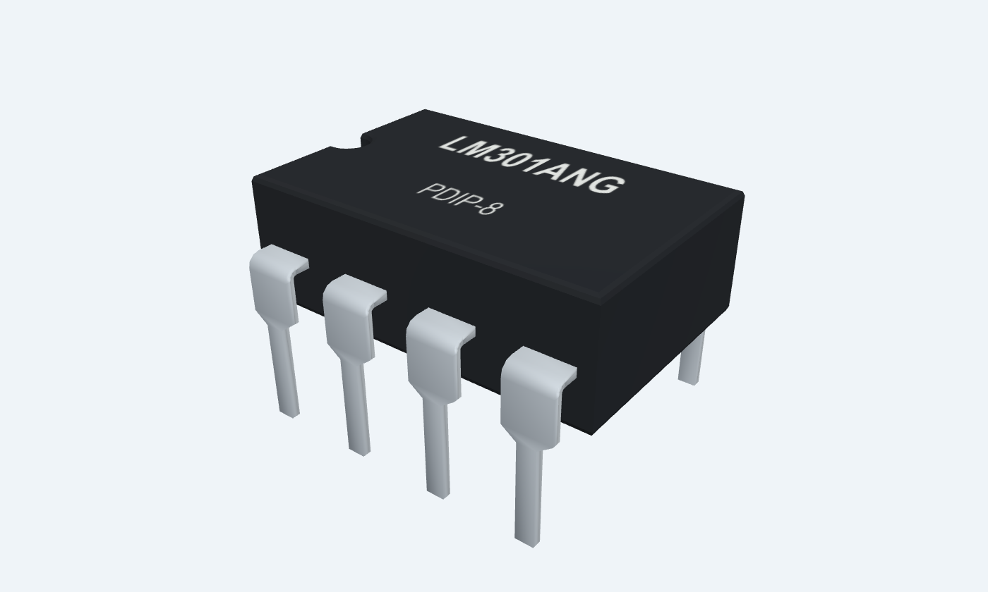
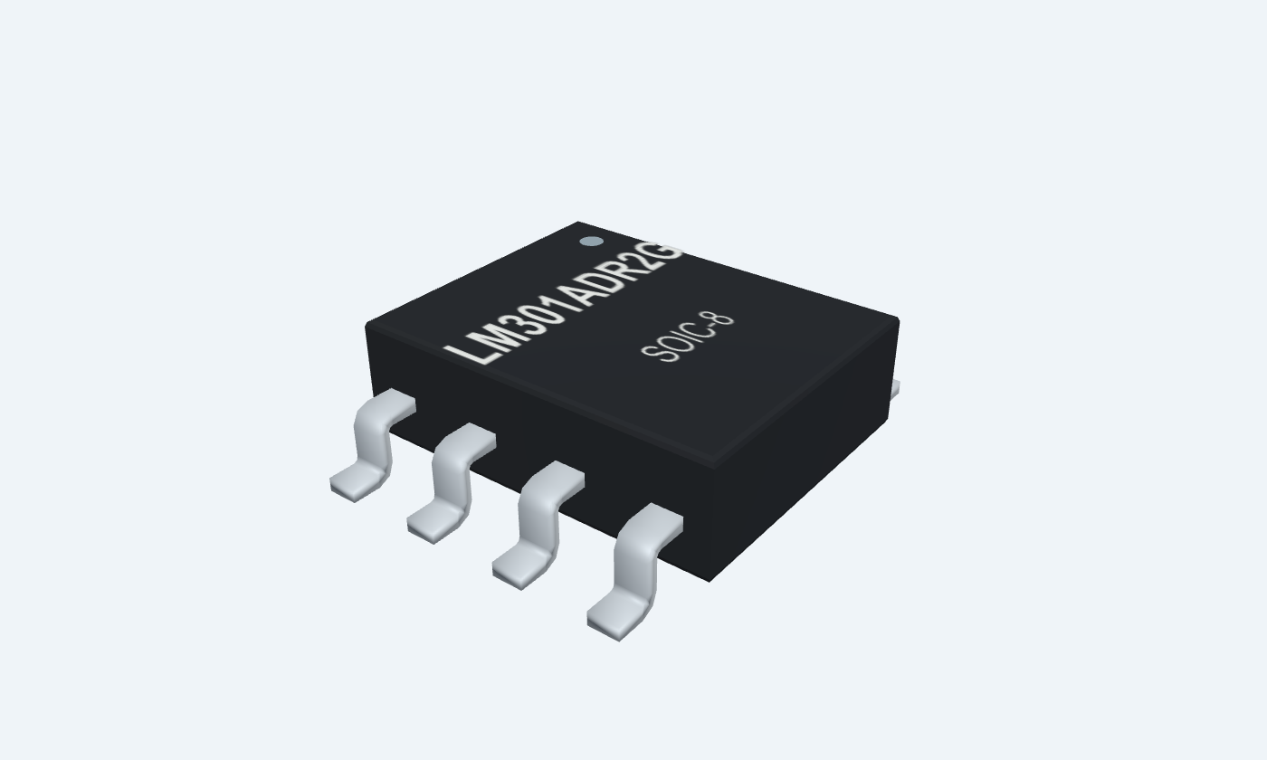

8Physical pins
LM301ANGPDIP-8
Manufacturer-referencedonsemi
Pin diagram
Select a pin to explore its connection
Highlight
LM301ANGPDIP-8Top view
LM301ASOIC-8Top view
Click a lead or use the arrow keys. Top view
PIN 1 · Balance / compensation
Balance / compensationBAL1
Function
One balance node also used by the external compensation network.
How to connect
Connect a 30 pF capacitor to pin 8 in this example.
Electrical note
Do not leave the compensation path out.
PIN 2 · Signal inputs
Inverting inputIN−
Function
Negative-feedback input.
How to connect
Join the 90 kΩ feedback and 10 kΩ ground resistors.
PIN 3 · Signal inputs
Non-inverting inputIN+
Function
Positive signal input.
How to connect
Apply 0.20 V relative to the supply midpoint.
PIN 4 · Supply
Negative supplyVEE
Function
Negative power rail.
How to connect
Connect to −15 V and bypass to the 0 V midpoint.
PIN 5 · Balance / compensation
BalanceBAL2
Function
Other offset-balance node.
How to connect
Leave open when optional offset adjustment is not fitted.
PIN 6 · Analog output
Analog outputOUT
Function
Class AB amplifier output.
How to connect
Connect 90 kΩ to IN− and a high-impedance meter.
Electrical note
Not rail-to-rail.
PIN 7 · Supply
Positive supplyVCC
Function
Positive power rail.
How to connect
Connect to +15 V and bypass locally to midpoint.
PIN 8 · Balance / compensation
CompensationCOMP
Function
External frequency-compensation connection.
How to connect
Connect 30 pF between pins 8 and 1.
Electrical note
This pin is functional; it is not NC as on some other eight-pin amplifiers.
Key specifications
Use the LM301A column of the shared family datasheet. The higher supply and temperature ratings of LM201A/LM201AV do not apply.
External compensation30 pF · example
Example rails±15 V
LM301A ambient0–70 °C
Example gain10 V/V
Package details
LM301ANG · PDIP-8
| Property | Details |
|---|---|
| Manufacturer | onsemi |
| Part number | LM301ANG |
| Package | PDIP-8 |
| Connections | 8 pins |
| Mounting | Through-hole |
| Lead pitch | 2.54 mm |
| Package code | CASE 626-05 |
| Thermal reference | Check package dissipation and actual mounting |
Device and package scope
onsemi revision 12
Manufacturer specifications 5 parameters
Scroll sideways to see all columns.
| Parameter | Value | Conditions / notes |
|---|---|---|
| SOIC-8 order | LM301ADR2G | Tape and reel; listed order |
| PDIP-8 order | LM301ANG | Legacy, marked discontinued in revision 12 |
| Compensation | External | Pin 1 to pin 8 for single-pole scheme |
| Ambient range | 0 to +70°C | LM301A grade |
| Supply specification range | ±5 to ±15 V | Unless a specific test states otherwise |
No specifications match. Try a parameter name or a unit.
Do not combine different family-member limits.
DC electrical characteristics
LM301A · 25°C unless stated
Manufacturer specifications 6 parameters
Scroll sideways to see all columns.
| Parameter | Value | Conditions / notes |
|---|---|---|
| Input offset | 2 mV typical; 7.5 mV maximum | RS ≤ 50 kΩ |
| Input offset current | 3 nA typical; 50 nA maximum | 25°C |
| Input bias current | 70 nA typical; 250 nA maximum | 25°C |
| Input resistance | 2 MΩ typical; 0.5 MΩ minimum | Specified test conditions |
| Supply current | 1.8 mA typical; 3 mA maximum | ±15 V |
| Open-loop gain | 160 V/mV typical; 25 minimum | ±15 V, VO ±10 V, RL > 2 kΩ |
No specifications match. Try a parameter name or a unit.
Typical values are not guarantees.
Across the operating temperature range
LM301A, 0 to +70°C
Manufacturer specifications 7 parameters
Scroll sideways to see all columns.
| Parameter | Value | Conditions / notes |
|---|---|---|
| Input offset | 10 mV maximum | RS ≤ 50 kΩ |
| Offset / bias current | 70 / 300 nA maximum | Specified family conditions |
| Input voltage range | −12 to +12 V | ±15 V rails |
| CMRR | 70 dB minimum; 90 typical | RS ≤ 50 kΩ |
| Supply rejection | 70 dB minimum; 96 typical | RS ≤ 50 kΩ |
| Output swing with 10 kΩ | ±12 V minimum; ±14 V typical | ±15 V supply |
| Output swing with >2 kΩ | ±10 V minimum; ±13 V typical | ±15 V supply |
No specifications match. Try a parameter name or a unit.
Leave input and output headroom.
Absolute maximum ratings
Stress limits, not operating targets
Manufacturer specifications 5 parameters
Scroll sideways to see all columns.
| Parameter | Value | Conditions / notes |
|---|---|---|
| Supply rails | ±18 V | LM301A, not LM201A |
| Differential input | ±30 V | Absolute limit |
| Common-mode stress | ±15 V | Below ±15 V supply, input limit equals supply |
| PDIP dissipation | 625 mW at ambient 25°C | Derate 5 mW/°C above 25°C |
| Storage | −65 to +150°C | Unpowered |
No specifications match. Try a parameter name or a unit.
Package and mounting constrain dissipation.
Gain-of-ten circuit
Light-load illustrative DC calculation
Manufacturer specifications 6 parameters
Scroll sideways to see all columns.
| Parameter | Value | Conditions / notes |
|---|---|---|
| Positive / negative rails | +15 V / −15 V | Pins 7 / 4; midpoint is 0 V |
| Compensation | 30 pF | Between pins 1 and 8 |
| Feedback / return | 90 kΩ / 10 kΩ | OUT6 to IN−2; IN−2 to midpoint |
| Input / ideal output | 0.20 V / 2.00 V | IN+3; high-impedance output meter |
| Supply bypass | 100 nF per rail | Each rail to midpoint |
| Balance pin 5 | Open | Optional trim not fitted |
No specifications match. Try a parameter name or a unit.
30 pF is a conservative standard compensation choice; dynamic behavior still needs validation.
Connections by function
Select a pin for its function, connection guidance and electrical notes.
Balance / compensation3 pins
Signal inputs2 pins
Supply2 pins
Analog output1 pin
Balance / compensation3 pins
Signal inputs2 pins
Supply2 pins
Analog output1 pin
LM301A at a glance
Follow the labeled connections and functional stages
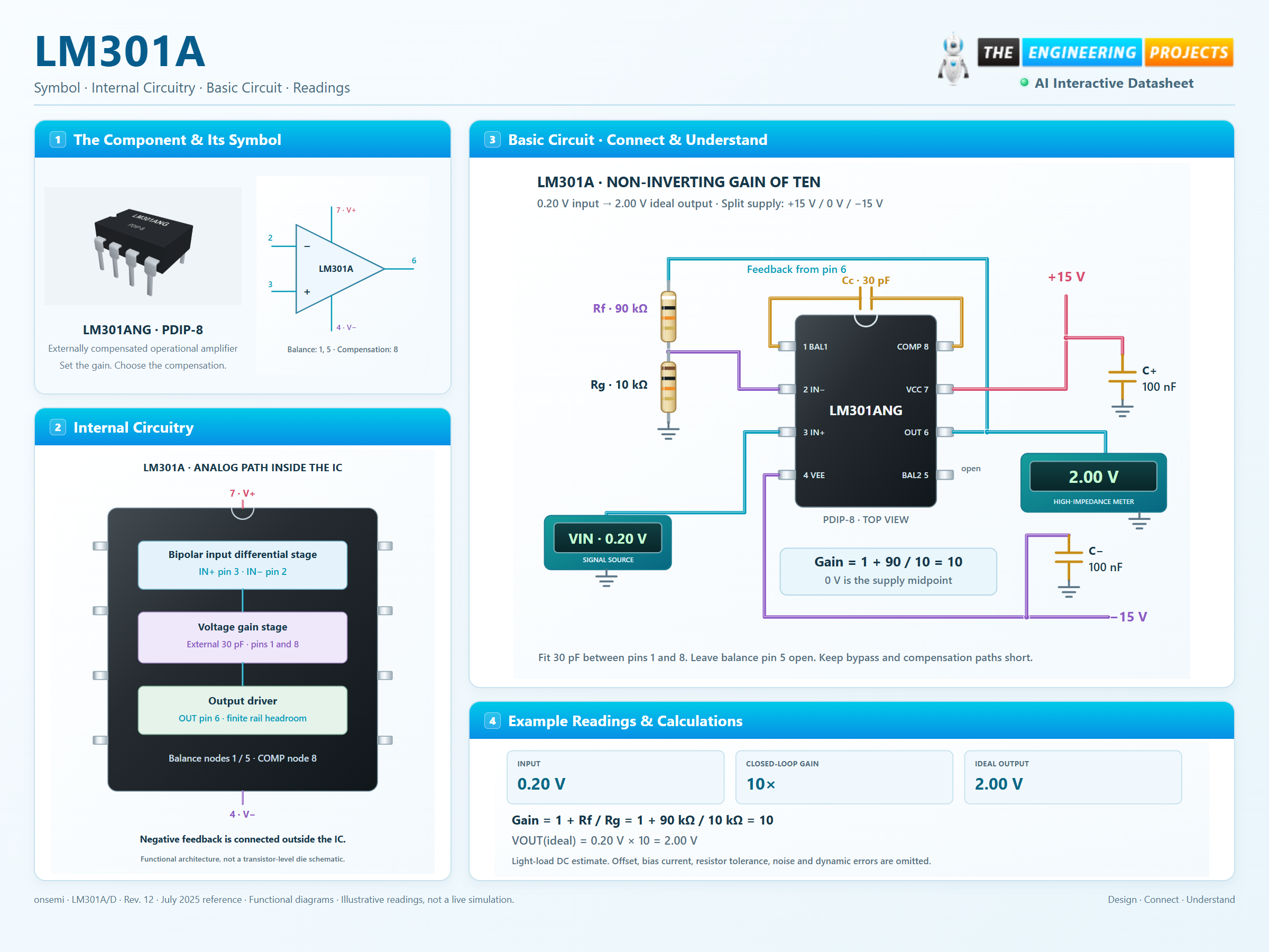
How it works
3 stages · Explore one step at a time
Compare the inputs
The differential stage responds to the voltage between IN+ and IN−.
Choose compensation
The external capacitor shapes loop response. The illustrated 30 pF connection is between pins 1 and 8; keep it short.
Close the feedback loop
Negative feedback makes the nominal DC gain 1 + 90 kΩ / 10 kΩ = 10. Real offset, bias current, bandwidth and loading cause error.
Step 1 of 3
LM301A in a circuit
Physical eight-pin IC, split rails and a visible 30 pF connection.
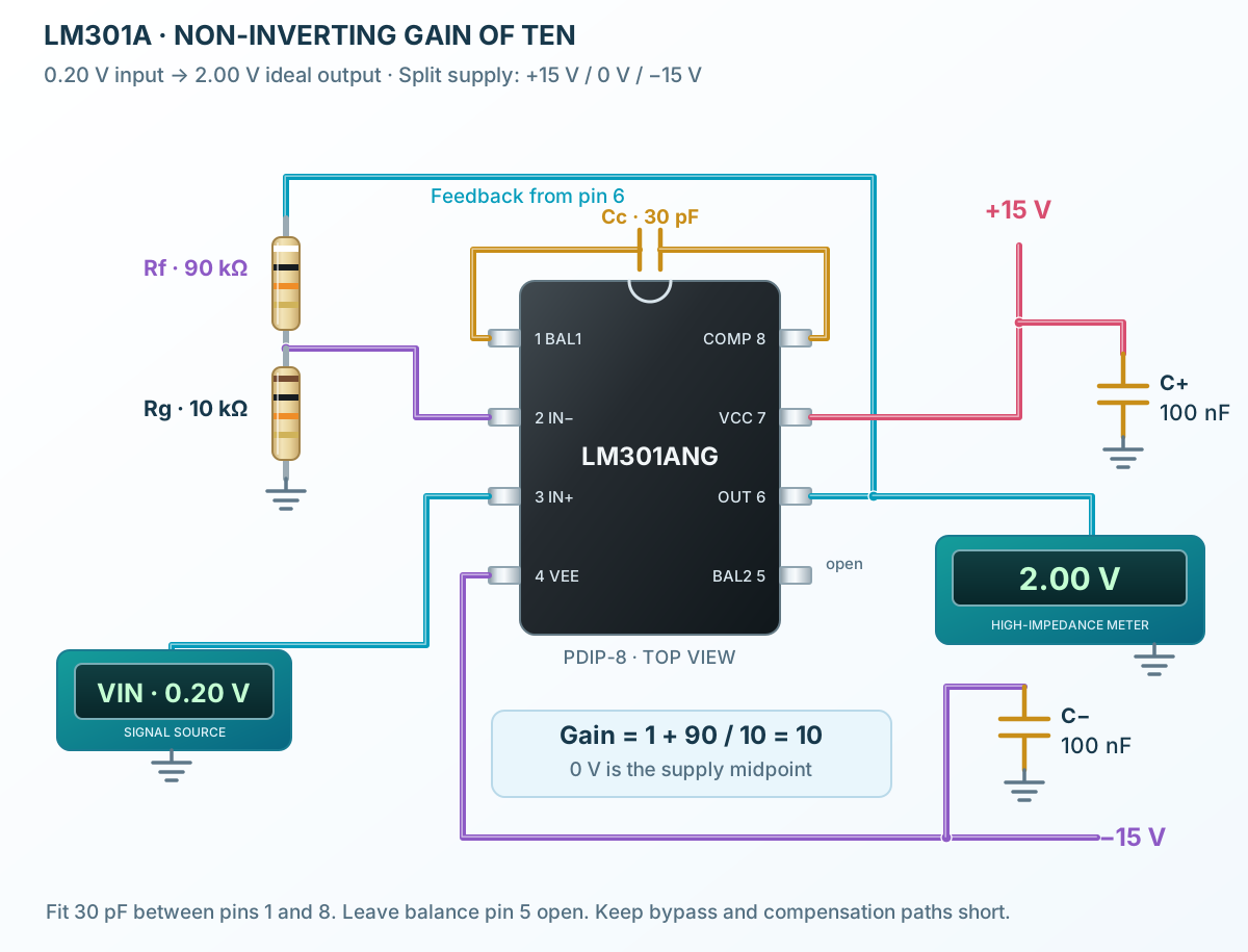
Connect it, step by step
Follow the component values and pin connections
Compare the inputs
The differential stage responds to the voltage between IN+ and IN−.
Choose compensation
The external capacitor shapes loop response. The illustrated 30 pF connection is between pins 1 and 8; keep it short.
Close the feedback loop
Negative feedback makes the nominal DC gain 1 + 90 kΩ / 10 kΩ = 10. Real offset, bias current, bandwidth and loading cause error.
Inside LM301A
Compact differential, gain and output stages inside the IC.
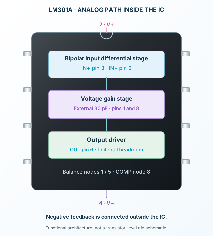
Explore the circuit
Select a stage to see its role and connections
Compare the inputs
The differential stage responds to the voltage between IN+ and IN−.
Choose compensation
The external capacitor shapes loop response. The illustrated 30 pF connection is between pins 1 and 8; keep it short.
Close the feedback loop
Negative feedback makes the nominal DC gain 1 + 90 kΩ / 10 kΩ = 10. Real offset, bias current, bandwidth and loading cause error.
Selected packagePDIP-8LM301ANG
Physical connections8 pinsPackage-specific numbering
Reference collection6 tables29 parameters & pin functions
Pin reference
Signal names, electrical functions and connection guidance
Physical pin numbers8 pins
Scroll within the table to see all columns and rows.
| Pin | Signal | Type | Function & connection |
|---|---|---|---|
| BAL1 | Balance / compensation | One balance node also used by the external compensation network.Connection guidanceConnect a 30 pF capacitor to pin 8 in this example. Do not leave the compensation path out. | |
| IN− | Inverting input | Negative-feedback input.Connection guidanceJoin the 90 kΩ feedback and 10 kΩ ground resistors. | |
| IN+ | Non-inverting input | Positive signal input.Connection guidanceApply 0.20 V relative to the supply midpoint. | |
| VEE | Negative supply | Negative power rail.Connection guidanceConnect to −15 V and bypass to the 0 V midpoint. | |
| BAL2 | Balance | Other offset-balance node.Connection guidanceLeave open when optional offset adjustment is not fitted. | |
| OUT | Analog output | Class AB amplifier output.Connection guidanceConnect 90 kΩ to IN− and a high-impedance meter. Not rail-to-rail. | |
| VCC | Positive supply | Positive power rail.Connection guidanceConnect to +15 V and bypass locally to midpoint. | |
| COMP | Compensation | External frequency-compensation connection.Connection guidanceConnect 30 pF between pins 8 and 1. This pin is functional; it is not NC as on some other eight-pin amplifiers. |
No pins match these filters. Try another signal name or reset the filters.
Device and package scope
onsemi revision 12
Manufacturer-referenced values5 parameters
Scroll within the table to see all columns and rows.
| Parameter | Value | Conditions / notes |
|---|---|---|
| SOIC-8 order | LM301ADR2G | Tape and reel; listed order |
| PDIP-8 order | LM301ANG | Legacy, marked discontinued in revision 12 |
| Compensation | External | Pin 1 to pin 8 for single-pole scheme |
| Ambient range | 0 to +70°C | LM301A grade |
| Supply specification range | ±5 to ±15 V | Unless a specific test states otherwise |
No specifications match. Try a parameter name or a unit.
Do not combine different family-member limits.
DC electrical characteristics
LM301A · 25°C unless stated
Manufacturer-referenced values6 parameters
Scroll within the table to see all columns and rows.
| Parameter | Value | Conditions / notes |
|---|---|---|
| Input offset | 2 mV typical; 7.5 mV maximum | RS ≤ 50 kΩ |
| Input offset current | 3 nA typical; 50 nA maximum | 25°C |
| Input bias current | 70 nA typical; 250 nA maximum | 25°C |
| Input resistance | 2 MΩ typical; 0.5 MΩ minimum | Specified test conditions |
| Supply current | 1.8 mA typical; 3 mA maximum | ±15 V |
| Open-loop gain | 160 V/mV typical; 25 minimum | ±15 V, VO ±10 V, RL > 2 kΩ |
No specifications match. Try a parameter name or a unit.
Typical values are not guarantees.
Across the operating temperature range
LM301A, 0 to +70°C
Manufacturer-referenced values7 parameters
Scroll within the table to see all columns and rows.
| Parameter | Value | Conditions / notes |
|---|---|---|
| Input offset | 10 mV maximum | RS ≤ 50 kΩ |
| Offset / bias current | 70 / 300 nA maximum | Specified family conditions |
| Input voltage range | −12 to +12 V | ±15 V rails |
| CMRR | 70 dB minimum; 90 typical | RS ≤ 50 kΩ |
| Supply rejection | 70 dB minimum; 96 typical | RS ≤ 50 kΩ |
| Output swing with 10 kΩ | ±12 V minimum; ±14 V typical | ±15 V supply |
| Output swing with >2 kΩ | ±10 V minimum; ±13 V typical | ±15 V supply |
No specifications match. Try a parameter name or a unit.
Leave input and output headroom.
Absolute maximum ratings
Stress limits, not operating targets
Manufacturer-referenced values5 parameters
Scroll within the table to see all columns and rows.
| Parameter | Value | Conditions / notes |
|---|---|---|
| Supply rails | ±18 V | LM301A, not LM201A |
| Differential input | ±30 V | Absolute limit |
| Common-mode stress | ±15 V | Below ±15 V supply, input limit equals supply |
| PDIP dissipation | 625 mW at ambient 25°C | Derate 5 mW/°C above 25°C |
| Storage | −65 to +150°C | Unpowered |
No specifications match. Try a parameter name or a unit.
Package and mounting constrain dissipation.
Gain-of-ten circuit
Light-load illustrative DC calculation
Manufacturer-referenced values6 parameters
Scroll within the table to see all columns and rows.
| Parameter | Value | Conditions / notes |
|---|---|---|
| Positive / negative rails | +15 V / −15 V | Pins 7 / 4; midpoint is 0 V |
| Compensation | 30 pF | Between pins 1 and 8 |
| Feedback / return | 90 kΩ / 10 kΩ | OUT6 to IN−2; IN−2 to midpoint |
| Input / ideal output | 0.20 V / 2.00 V | IN+3; high-impedance output meter |
| Supply bypass | 100 nF per rail | Each rail to midpoint |
| Balance pin 5 | Open | Optional trim not fitted |
No specifications match. Try a parameter name or a unit.
30 pF is a conservative standard compensation choice; dynamic behavior still needs validation.
No matching rowsTry a pin name, parameter, unit or test condition, or reset the filters.
Analog feedback
Build low-frequency gain stages within the common-mode and output limits.
Manufacturer application guideSumming circuits
Use an appropriate feedback network and deliberately selected compensation.
Manufacturer application guideControl-loop study
Explore the relationship between external compensation, gain and transient response.
Manufacturer application guideTake it into ProTech
Find LM301A in the Components Library to place its schematic symbol and connect its pins.
Reference page · circuit simulation model not yet availableOpen ProTech