Real View
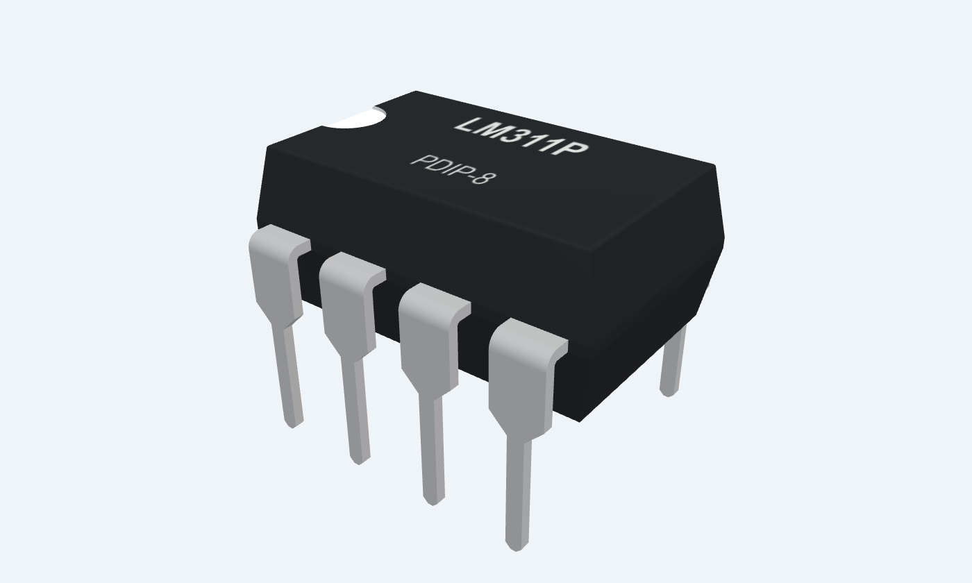
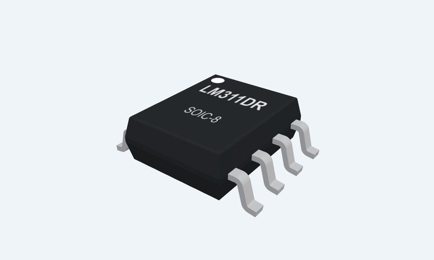
A fast voltage decision with a flexible output transistor.
LM311 is a single voltage comparator with separately accessible collector and emitter output pins. It compares two input voltages and switches its output transistor rather than amplifying a signal linearly. Our 5 V example compares VIN with a 2 V resistor reference. The emitter is grounded and the collector uses a 10 kΩ pull-up, giving a LOW output below the threshold and a HIGH output above it. Balance and strobe contacts add flexibility, but they require the correct external network. This reference follows TI’s commercial LM311P and LM311DR with both optional contacts left open in the basic circuit.
Select a pin to explore its connection
Click a lead or use the arrow keys. Top view
Emitter of the output transistor, separate from the negative supply.
Connect to ground for the illustrated logic output.
Do not leave the emitter floating.
Signal input in the threshold detector.
Connect VIN; keep it within 0.5–3.5 V for the 5 V example.
Reference input in the threshold detector.
Connect the 2.00 V divider node.
Negative power rail for the comparator.
Connect to ground in the single-supply example.
This is a supply pin; it is not internally interchangeable with output emitter pin 1.
Optional offset-balance connection.
Leave open when offset trimming is not used.
Optional balance and current-driven output-disable connection.
Leave open in this unstrobbed circuit.
Do not short to ground. Use the manufacturer’s current-driven strobe network when required.
Collector of the output transistor.
Add 10 kΩ to +5 V and read this node.
HIGH requires an external pull-up; this pin sinks current when the transistor is on.
Positive comparator supply.
Connect +5 V with 100 nF bypass to pin 4.
The output collector and emitter are both exposed. The chosen emitter return and external pull-up determine the logic levels.
LM311P · PDIP-8
| Property | Details |
|---|---|
| Manufacturer | Texas Instruments |
| Part number | LM311P |
| Package | PDIP-8 |
| Connections | 8 pins |
| Mounting | Through-hole |
| Lead pitch | 2.54 mm |
| Package code | dip |
| Thermal reference | Board and package dependent; see manufacturer data |
TI LM311 commercial grade
Scroll sideways to see all columns.
| Parameter | Value | Conditions / notes |
|---|---|---|
| Supply span | 3.5–30 V | V+ minus V− |
| Ambient range | 0 to +70°C | LM311 grade |
| Recommended input range | V− + 0.5 V to V+ − 1.5 V | Subject to the manufacturer supply conditions |
| Inputs in the 5 V example | 0.5–3.5 V | Both VIN and VREF |
| Balance / strobe | Open in the basic circuit | Optional networks shown in the manufacturer PDF |
No specifications match. Try a parameter name or a unit.
Supply range and input range are separate constraints.
±15 V test supply unless stated
Scroll sideways to see all columns.
| Parameter | Value | Conditions / notes |
|---|---|---|
| Input offset voltage | 2 mV typical; 7.5 mV maximum | 25°C; 10 mV maximum over temperature |
| Input bias current | 100 nA typical; 250 nA maximum | 25°C; 300 nA maximum over temperature |
| Input offset current | 6 nA typical; 50 nA maximum | 25°C; 70 nA maximum over temperature |
| Collector-emitter LOW | 0.23 V typical; 0.4 V maximum | 4.5 V single supply; 8 mA sink; VID = −10 mV |
| Positive supply current | 5.1 mA typical; 7.5 mA maximum | Output LOW; no load; 25°C |
| Negative supply current magnitude | 4.1 mA typical; 5 mA maximum | Output HIGH; no load; 25°C |
No specifications match. Try a parameter name or a unit.
The LOW-voltage test is load dependent. It is not a fixed voltage for every collector current.
Manufacturer switching test
Scroll sideways to see all columns.
| Parameter | Value | Conditions / notes |
|---|---|---|
| LOW-to-HIGH response | 115 ns typical | ±15 V supply; 100 mV step; 5 mV overdrive |
| HIGH-to-LOW response | 165 ns typical | Same step and overdrive |
| Test output load | 500 Ω to 5 V; 5 pF | Different loading changes delay |
| VIN below VREF | Output transistor ON | Collector pulled toward emitter |
| VIN above VREF | Output transistor OFF | Pull-up creates HIGH |
| No pull-up, output OFF | Floating collector | Not a valid HIGH |
No specifications match. Try a parameter name or a unit.
Near equality, offset and noise can dominate. Typical response is not a guaranteed delay.
A 2.00 V reference and 10 kΩ pull-up
Scroll sideways to see all columns.
| Parameter | Value | Conditions / notes |
|---|---|---|
| Reference upper resistor | 30 kΩ | +5 V to VREF |
| Reference lower resistor | 20 kΩ | VREF to ground |
| Reference result | 2.00 V | 5 × 20 / (30 + 20) |
| Signal input | 1.50 V initially | IN+ pin 2 |
| Output pull-up | 10 kΩ | +5 V to collector pin 7 |
| Emitter and negative rail | Pins 1 and 4 to ground | Two distinct terminals |
| Supply bypass | 100 nF | Pins 8–4; short local loop |
No specifications match. Try a parameter name or a unit.
The high-impedance output meter adds negligible loading.
LM311P · PDIP-8
Scroll sideways to see all columns.
| Parameter | Value | Conditions / notes |
|---|---|---|
| Offset trim | Balance pins 5 and 6 | Use the manufacturer network |
| Strobe drive | Current driven, approximately −3 to −5 mA | Do not short the strobe contact to ground |
| Supply absolute maximum | 36 V total | Stress only; recommended maximum 30 V |
| Collector to V− absolute maximum | 40 V for LM311 | The 50 V rating belongs to other family members |
| Storage temperature | −65 to +150°C | Unpowered storage |
| Pin pitch | 2.54 mm | Through-hole |
No specifications match. Try a parameter name or a unit.
Stress ratings do not describe recommended continuous operation.
Select a pin for its function, connection guidance and electrical notes.
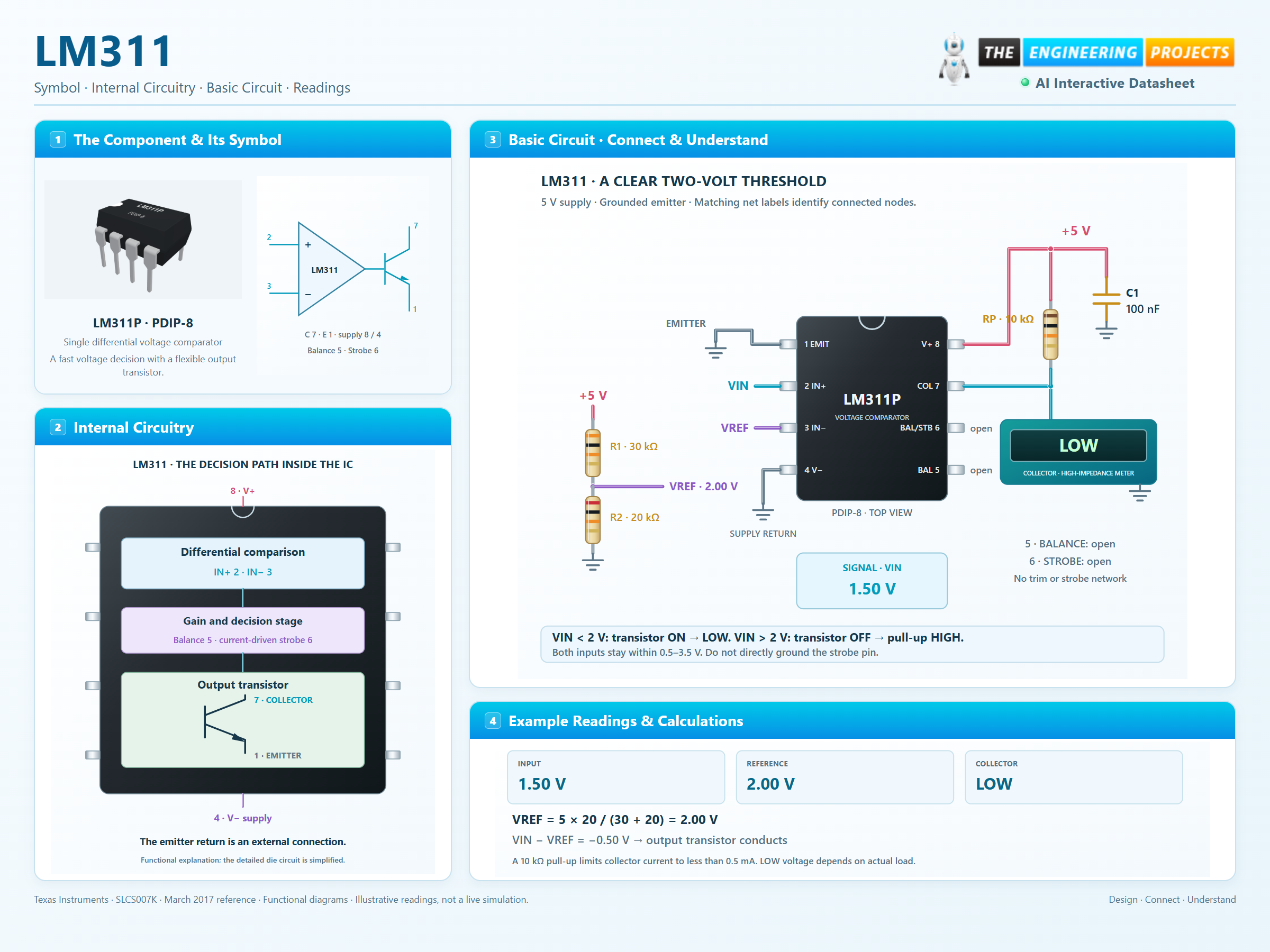
Follow the labeled connections and functional stages
3 stages · Explore one step at a time
VIN enters IN+ pin 2; the 2 V reference enters IN− pin 3. Their difference determines the unstrobbed output state.
Below the threshold, the transistor conducts from collector pin 7 to emitter pin 1. Above it, the transistor releases the collector and the pull-up establishes HIGH.
Offset creates uncertainty around equality. Positive-feedback hysteresis can stabilize a noisy threshold; it is not included in this simple example.
Adjust VIN and the reference. Remove the pull-up to see why it matters.
Enable JavaScript to explore the comparator.
Violet: offset-sensitive transition · Amber: input outside the recommended range.
Unstrobed DC teaching model with emitter pin 1 grounded. Valid input range is 0.5–3.5 V. The ±10 mV uncertainty band follows the full-temperature offset limit; it is not hysteresis. LOW uses an illustrative 0.23 V estimate from a different test load. Actual saturation, transient delay, leakage and noise are omitted.
Separate emitter return, reference divider and collector pull-up.
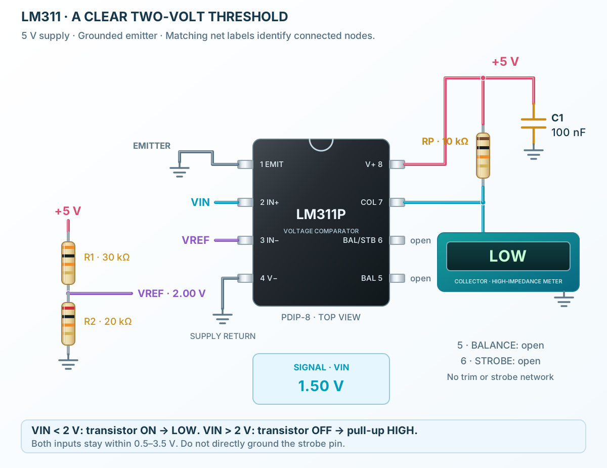
Follow the component values and pin connections
30 kΩ over 20 kΩ gives 2 V from 5 V.
Ground pin 4 for power and pin 1 for the output transistor. Add 100 nF supply bypass.
Add 10 kΩ to +5 V at pin 7. VIN below 2 V gives LOW; above 2 V gives HIGH.
A differential decision stage and an accessible output transistor.
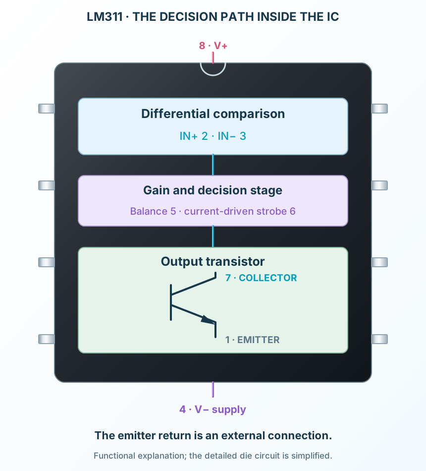
Select a stage to see its role and connections
Compare the input voltages within the permitted common-mode range.
Optional external networks adjust offset or release the output. Their electrical drive requirements matter.
The output transistor has both contacts available. The external circuit sets its return and HIGH level.
Signal names, electrical functions and connection guidance
Scroll within the table to see all columns and rows.
| Pin | Signal | Type | Function & connection |
|---|---|---|---|
| EMIT | Output emitter | Emitter of the output transistor, separate from the negative supply.Connection guidanceConnect to ground for the illustrated logic output. Do not leave the emitter floating. | |
| IN+ | Non-inverting input | Signal input in the threshold detector.Connection guidanceConnect VIN; keep it within 0.5–3.5 V for the 5 V example. | |
| IN− | Inverting input | Reference input in the threshold detector.Connection guidanceConnect the 2.00 V divider node. | |
| V− | Negative supply | Negative power rail for the comparator.Connection guidanceConnect to ground in the single-supply example. This is a supply pin; it is not internally interchangeable with output emitter pin 1. | |
| BAL | Offset balance | Optional offset-balance connection.Connection guidanceLeave open when offset trimming is not used. | |
| BAL/STB | Balance / strobe | Optional balance and current-driven output-disable connection.Connection guidanceLeave open in this unstrobbed circuit. Do not short to ground. Use the manufacturer’s current-driven strobe network when required. | |
| COL | Output collector | Collector of the output transistor.Connection guidanceAdd 10 kΩ to +5 V and read this node. HIGH requires an external pull-up; this pin sinks current when the transistor is on. | |
| V+ | Positive supply | Positive comparator supply.Connection guidanceConnect +5 V with 100 nF bypass to pin 4. |
No pins match these filters. Try another signal name or reset the filters.
TI LM311 commercial grade
Scroll within the table to see all columns and rows.
| Parameter | Value | Conditions / notes |
|---|---|---|
| Supply span | 3.5–30 V | V+ minus V− |
| Ambient range | 0 to +70°C | LM311 grade |
| Recommended input range | V− + 0.5 V to V+ − 1.5 V | Subject to the manufacturer supply conditions |
| Inputs in the 5 V example | 0.5–3.5 V | Both VIN and VREF |
| Balance / strobe | Open in the basic circuit | Optional networks shown in the manufacturer PDF |
No specifications match. Try a parameter name or a unit.
Supply range and input range are separate constraints.
±15 V test supply unless stated
Scroll within the table to see all columns and rows.
| Parameter | Value | Conditions / notes |
|---|---|---|
| Input offset voltage | 2 mV typical; 7.5 mV maximum | 25°C; 10 mV maximum over temperature |
| Input bias current | 100 nA typical; 250 nA maximum | 25°C; 300 nA maximum over temperature |
| Input offset current | 6 nA typical; 50 nA maximum | 25°C; 70 nA maximum over temperature |
| Collector-emitter LOW | 0.23 V typical; 0.4 V maximum | 4.5 V single supply; 8 mA sink; VID = −10 mV |
| Positive supply current | 5.1 mA typical; 7.5 mA maximum | Output LOW; no load; 25°C |
| Negative supply current magnitude | 4.1 mA typical; 5 mA maximum | Output HIGH; no load; 25°C |
No specifications match. Try a parameter name or a unit.
The LOW-voltage test is load dependent. It is not a fixed voltage for every collector current.
Manufacturer switching test
Scroll within the table to see all columns and rows.
| Parameter | Value | Conditions / notes |
|---|---|---|
| LOW-to-HIGH response | 115 ns typical | ±15 V supply; 100 mV step; 5 mV overdrive |
| HIGH-to-LOW response | 165 ns typical | Same step and overdrive |
| Test output load | 500 Ω to 5 V; 5 pF | Different loading changes delay |
| VIN below VREF | Output transistor ON | Collector pulled toward emitter |
| VIN above VREF | Output transistor OFF | Pull-up creates HIGH |
| No pull-up, output OFF | Floating collector | Not a valid HIGH |
No specifications match. Try a parameter name or a unit.
Near equality, offset and noise can dominate. Typical response is not a guaranteed delay.
A 2.00 V reference and 10 kΩ pull-up
Scroll within the table to see all columns and rows.
| Parameter | Value | Conditions / notes |
|---|---|---|
| Reference upper resistor | 30 kΩ | +5 V to VREF |
| Reference lower resistor | 20 kΩ | VREF to ground |
| Reference result | 2.00 V | 5 × 20 / (30 + 20) |
| Signal input | 1.50 V initially | IN+ pin 2 |
| Output pull-up | 10 kΩ | +5 V to collector pin 7 |
| Emitter and negative rail | Pins 1 and 4 to ground | Two distinct terminals |
| Supply bypass | 100 nF | Pins 8–4; short local loop |
No specifications match. Try a parameter name or a unit.
The high-impedance output meter adds negligible loading.
LM311P · PDIP-8
Scroll within the table to see all columns and rows.
| Parameter | Value | Conditions / notes |
|---|---|---|
| Offset trim | Balance pins 5 and 6 | Use the manufacturer network |
| Strobe drive | Current driven, approximately −3 to −5 mA | Do not short the strobe contact to ground |
| Supply absolute maximum | 36 V total | Stress only; recommended maximum 30 V |
| Collector to V− absolute maximum | 40 V for LM311 | The 50 V rating belongs to other family members |
| Storage temperature | −65 to +150°C | Unpowered storage |
| Pin pitch | 2.54 mm | Through-hole |
No specifications match. Try a parameter name or a unit.
Stress ratings do not describe recommended continuous operation.
No matching rowsTry a pin name, parameter, unit or test condition, or reset the filters.
Turn a suitable sensor voltage into a logic decision with a defined pull-up.
Manufacturer application guideCombine feedback and timing networks, including hysteresis and the actual propagation delay.
Manufacturer application guideChoose collector pull-up and emitter return to suit the receiving logic while observing every voltage/current limit.
Manufacturer application guideFind LM311 in the Components Library to place its schematic symbol and connect its pins.
Reference page · circuit simulation model not yet availableOpen ProTech