 BETA
LM311 Working Principle
Learn how LM311 works with an illustrated explanation and practical readings.
LM311 at a glance
Follow the labeled connections and functional stages
How it works
3 stages · Explore one step at a time
Compare VIN and VREF
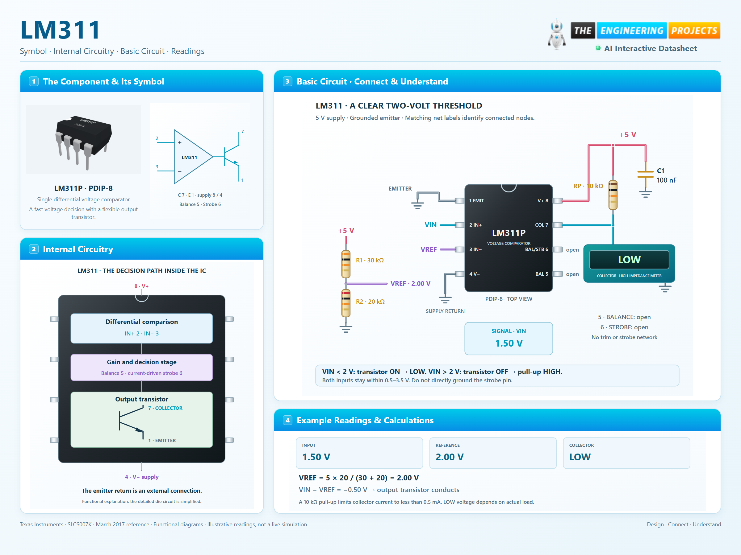
VIN enters IN+ pin 2; the 2 V reference enters IN− pin 3. Their difference determines the unstrobbed output state.
Switch the output transistor
Below the threshold, the transistor conducts from collector pin 7 to emitter pin 1. Above it, the transistor releases the collector and the pull-up establishes HIGH.
Control the transition
Offset creates uncertainty around equality. Positive-feedback hysteresis can stabilize a noisy threshold; it is not included in this simple example.
Find the switching threshold
Adjust VIN and the reference. Remove the pull-up to see why it matters.
Enable JavaScript to explore the comparator.
Violet: offset-sensitive transition · Amber: input outside the recommended range.
Unstrobed DC teaching model with emitter pin 1 grounded. Valid input range is 0.5–3.5 V. The ±10 mV uncertainty band follows the full-temperature offset limit; it is not hysteresis. LOW uses an illustrative 0.23 V estimate from a different test load. Actual saturation, transient delay, leakage and noise are omitted.