Real View
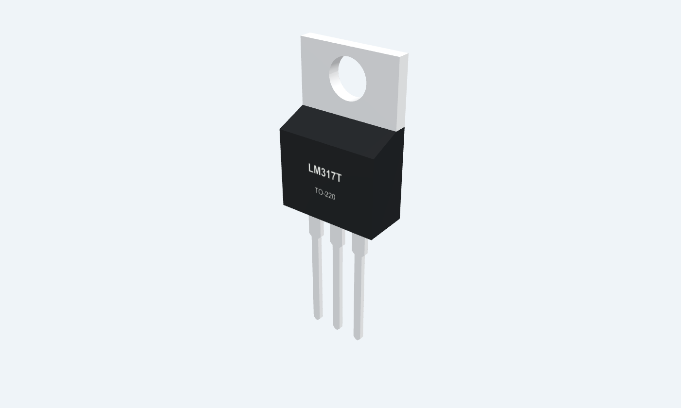
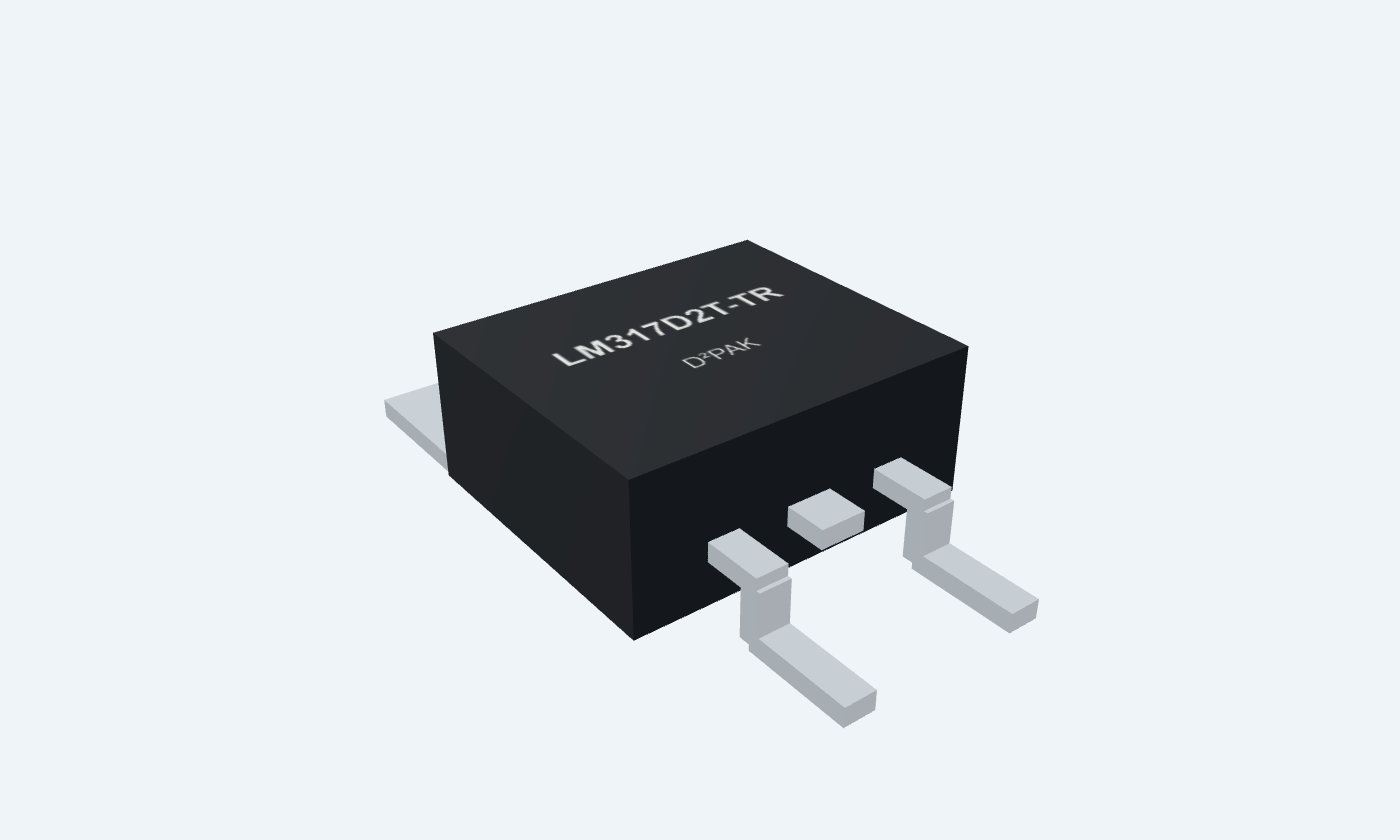
Set the voltage. Understand the heat.
LM317 is a three-terminal adjustable linear regulator. Two external resistors set its output, while an internal reference and pass stage maintain approximately 1.25 V between OUTPUT and ADJUST. This reference follows STMicroelectronics LM317T and LM317D2T-TR. Its output can be adjusted over the manufacturer’s 1.2–37 V range when input headroom, minimum load and thermal conditions are met. The metal tab is connected to OUTPUT. A useful design starts with the feedback equation, then checks bypass capacitors, load current and heat. The current rating alone does not determine how much power the package can dissipate.
Select a pin to explore its connection
Click a lead or use the arrow keys. Front view · marking toward you · leads down
The control loop holds approximately 1.25 V between OUTPUT and ADJUST.
Connect R1 from OUTPUT to ADJUST and R2 from ADJUST to the load return.
Adjustment current flows out of this pin; include IADJ × R2 when estimating output voltage. This is not a ground pin.
Supplies the load and the external feedback divider. The metal tab is also OUTPUT.
Connect the load and the top of R1 here. Keep the R1 connection close to the output lead.
The exposed TO-220 tab and D²PAK thermal pad are electrically live at output voltage; isolate a grounded heatsink where needed.
Feeds the pass stage from a DC voltage sufficiently above the requested output.
Place a 0.1 µF input bypass close to the device when required by the supply wiring.
The 40 V absolute limit is input-to-output differential, not a recommended operating input or an unconditional output range.
The regulated quantity is the voltage between OUTPUT and ADJUST. The external divider determines the output relative to ground.
LM317T · TO-220
| Property | Details |
|---|---|
| Manufacturer | STMicroelectronics |
| Part number | LM317T |
| Package | TO-220 |
| Connections | 3 pins |
| Mounting | Through-hole |
| Lead pitch | 2.54 mm |
| Package code | T |
| Thermal reference | Cooling and mounting dependent; see DS0433 |
ST LM317 · not LM217 or LM317B
Scroll sideways to see all columns.
| Parameter | Value | Conditions / notes |
|---|---|---|
| Output adjustment | 1.2–37 V | Requires input headroom, load and suitable cooling |
| Reference voltage | 1.2 / 1.25 / 1.3 V | Minimum / typical / maximum; Table 4 conditions |
| Junction temperature | 0–125°C | Selected LM317 grade |
| Minimum load at 40 V differential | 3.5 mA typical; 10 mA maximum | Output may rise if the load is insufficient |
| Adjustment current | 50 µA typical; 100 µA maximum | Include its contribution through R2 |
No specifications match. Try a parameter name or a unit.
Base conditions: VIN − VOUT = 5 V, IOUT = 500 mA, IMAX = 1.5 A, PMAX = 20 W unless stated. These are test conditions, not a package dissipation guarantee.
Manufacturer conditions retained
Scroll sideways to see all columns.
| Parameter | Value | Conditions / notes |
|---|---|---|
| Line regulation at 25°C | 0.01%/V typical; 0.04%/V maximum | VIN − VOUT = 3–40 V |
| Line regulation over temperature | 0.02%/V typical; 0.07%/V maximum | VIN − VOUT = 3–40 V |
| Load regulation, output ≤5 V | 5 mV typical; 25 mV maximum | 25°C; IOUT = 10 mA to IMAX |
| Ripple rejection without CADJ | 65 dB typical | 120 Hz; 25°C |
| Ripple rejection with CADJ | 66 dB minimum; 80 dB typical | CADJ = 10 µF; 120 Hz; 25°C |
No specifications match. Try a parameter name or a unit.
The adjustable output and test load affect which row applies; consult Table 4 for complete conditions.
9 V input · 120 Ω / 360 Ω divider
Scroll sideways to see all columns.
| Parameter | Value | Conditions / notes |
|---|---|---|
| R1 · OUTPUT to ADJUST | 120 Ω | Reference current ≈ 1.25 / 120 = 10.42 mA |
| R2 · ADJUST to GND | 360 Ω | Nominal resistor ratio 3:1 |
| Ideal output | 5.00 V | 1.25 × (1 + 360 / 120) |
| Including typical IADJ | 5.018 V | Adds 50 µA × 360 Ω = 18 mV |
| Input bypass | 0.1 µF | Place close to the input and return |
| Output capacitor | 1 µF tantalum | Illustrative transient improvement from manufacturer guidance |
No specifications match. Try a parameter name or a unit.
Use resistor and capacitor ratings appropriate to the circuit. The drawing omits optional adjustment bypass and its associated protection diode.
Current ratings require cooling
Scroll sideways to see all columns.
| Parameter | Value | Conditions / notes |
|---|---|---|
| Pass-stage estimate | PD ≈ (VIN − VOUT) × IOUT | Include divider current in IOUT |
| TO-220 RθJC | 5°C/W | Package reference; actual mounting matters |
| D²PAK RθJC | 3°C/W | Package reference; actual PCB copper matters |
| Overload protections | Current, thermal and safe-area protection | Do not use protection as normal regulation |
| High differential voltage | Available current decreases | See manufacturer curves and operating limits |
No specifications match. Try a parameter name or a unit.
The LM317 is a linear regulator: excess voltage is dissipated rather than efficiently converted.
LM317T · TO-220
Scroll sideways to see all columns.
| Parameter | Value | Conditions / notes |
|---|---|---|
| Connections | 1 ADJUST · 2 OUTPUT · 3 INPUT | Follow the selected package orientation |
| Tab / thermal pad | OUTPUT · pin 2 | Not GND |
| Input-to-output absolute maximum | 40 V | Stress rating; not a normal design target |
| Storage temperature | −65 to +150°C | Unpowered |
| Lead pitch | 2.54 mm | Verify the selected manufacturer drawing |
No specifications match. Try a parameter name or a unit.
The same three numbers have different functions from a 7805. Do not substitute without checking connections.
Select a pin for its function, connection guidance and electrical notes.
Follow the labeled connections and functional stages
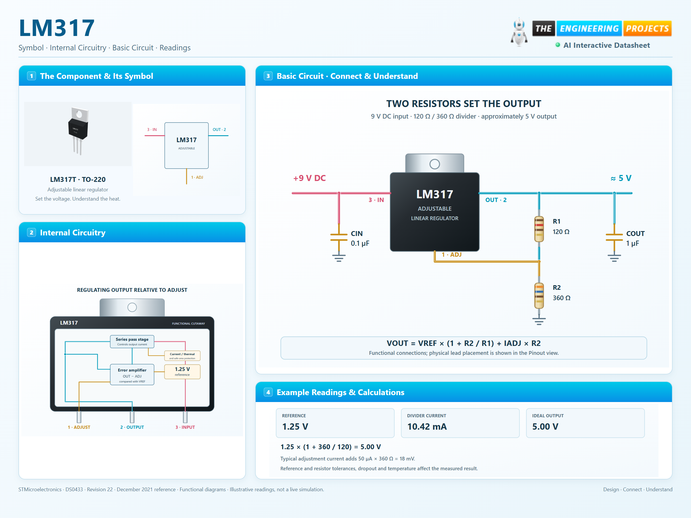
3 stages · Explore one step at a time
The regulator maintains approximately 1.25 V from OUTPUT to ADJUST. Unlike a 7805, the adjustment terminal is not tied directly to ground.
R1 runs from OUTPUT to ADJUST; R2 runs from ADJUST to the return. Their ratio sets the output, with a small additional term from adjustment-pin current.
The source must provide headroom and the load must draw sufficient current. Input-to-output voltage and current become heat in the pass stage.
One regulator, two resistors and short bypass connections.
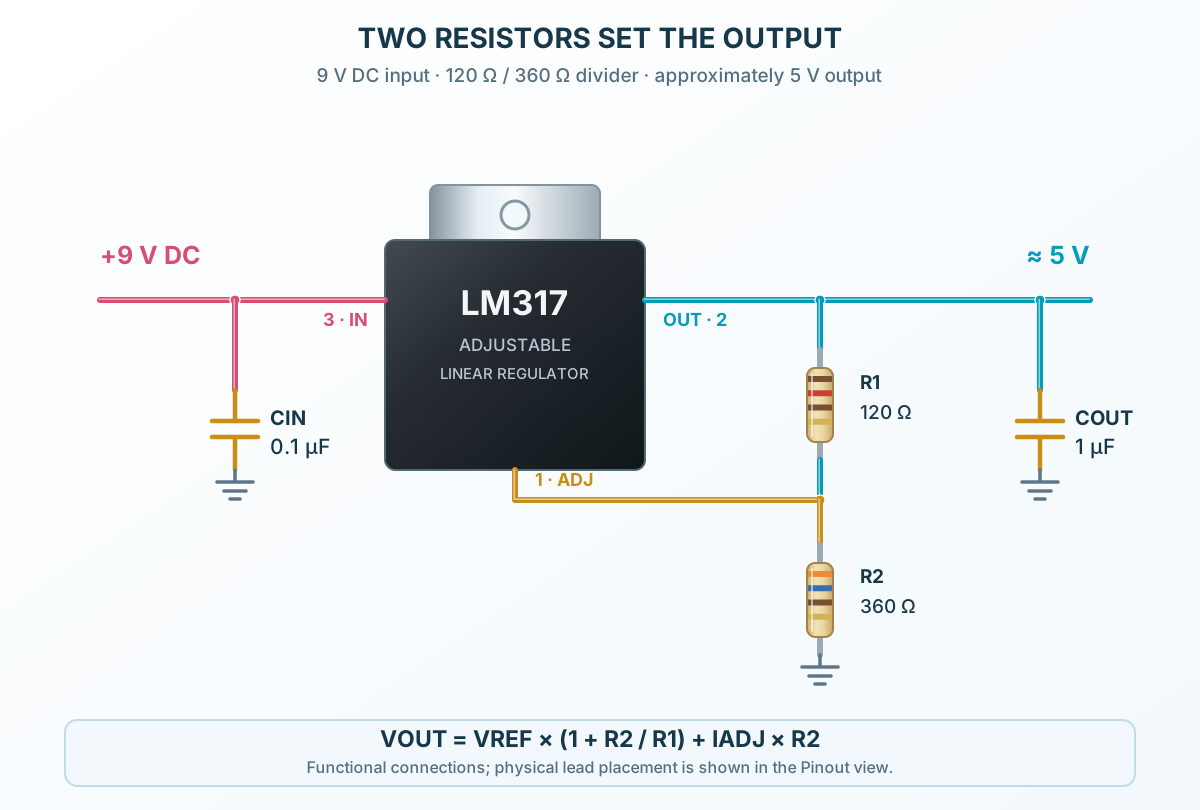
Follow the component values and pin connections
Feed INPUT from 9 V DC; put 0.1 µF between this rail and the common return.
R1 = 120 Ω goes from OUTPUT to ADJUST. R2 = 360 Ω goes from ADJUST to GND.
The ideal output is 5 V. Account for adjustment current and heating, then check it under the intended load.
A floating control loop inside the regulator package.
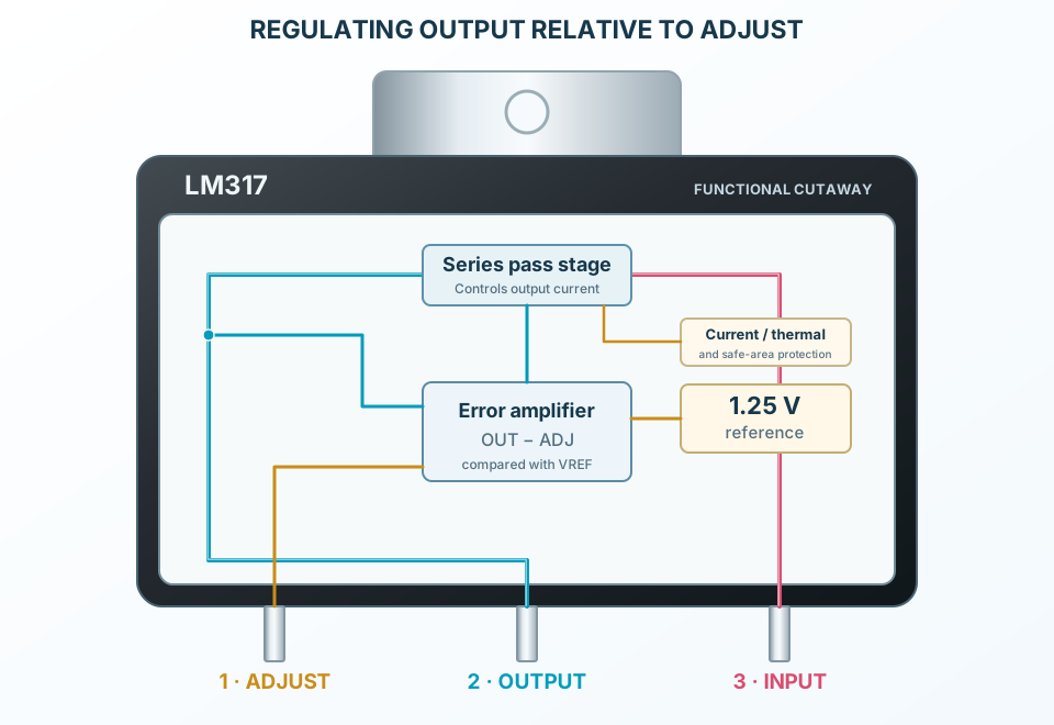
Select a stage to see its role and connections
The reference controls OUTPUT minus ADJUST; there is no dedicated ground lead.
The error amplifier drives the series pass stage to keep the reference difference stable.
Current and thermal limiting protect the pass stage under abnormal conditions.
Signal names, electrical functions and connection guidance
Scroll within the table to see all columns and rows.
| Pin | Signal | Type | Function & connection |
|---|---|---|---|
| ADJUST | Feedback reference | The control loop holds approximately 1.25 V between OUTPUT and ADJUST.Connection guidanceConnect R1 from OUTPUT to ADJUST and R2 from ADJUST to the load return. Adjustment current flows out of this pin; include IADJ × R2 when estimating output voltage. This is not a ground pin. | |
| OUTPUT | Regulated output | Supplies the load and the external feedback divider. The metal tab is also OUTPUT.Connection guidanceConnect the load and the top of R1 here. Keep the R1 connection close to the output lead. The exposed TO-220 tab and D²PAK thermal pad are electrically live at output voltage; isolate a grounded heatsink where needed. | |
| INPUT | Unregulated input | Feeds the pass stage from a DC voltage sufficiently above the requested output.Connection guidancePlace a 0.1 µF input bypass close to the device when required by the supply wiring. The 40 V absolute limit is input-to-output differential, not a recommended operating input or an unconditional output range. |
No pins match these filters. Try another signal name or reset the filters.
ST LM317 · not LM217 or LM317B
Scroll within the table to see all columns and rows.
| Parameter | Value | Conditions / notes |
|---|---|---|
| Output adjustment | 1.2–37 V | Requires input headroom, load and suitable cooling |
| Reference voltage | 1.2 / 1.25 / 1.3 V | Minimum / typical / maximum; Table 4 conditions |
| Junction temperature | 0–125°C | Selected LM317 grade |
| Minimum load at 40 V differential | 3.5 mA typical; 10 mA maximum | Output may rise if the load is insufficient |
| Adjustment current | 50 µA typical; 100 µA maximum | Include its contribution through R2 |
No specifications match. Try a parameter name or a unit.
Base conditions: VIN − VOUT = 5 V, IOUT = 500 mA, IMAX = 1.5 A, PMAX = 20 W unless stated. These are test conditions, not a package dissipation guarantee.
Manufacturer conditions retained
Scroll within the table to see all columns and rows.
| Parameter | Value | Conditions / notes |
|---|---|---|
| Line regulation at 25°C | 0.01%/V typical; 0.04%/V maximum | VIN − VOUT = 3–40 V |
| Line regulation over temperature | 0.02%/V typical; 0.07%/V maximum | VIN − VOUT = 3–40 V |
| Load regulation, output ≤5 V | 5 mV typical; 25 mV maximum | 25°C; IOUT = 10 mA to IMAX |
| Ripple rejection without CADJ | 65 dB typical | 120 Hz; 25°C |
| Ripple rejection with CADJ | 66 dB minimum; 80 dB typical | CADJ = 10 µF; 120 Hz; 25°C |
No specifications match. Try a parameter name or a unit.
The adjustable output and test load affect which row applies; consult Table 4 for complete conditions.
9 V input · 120 Ω / 360 Ω divider
Scroll within the table to see all columns and rows.
| Parameter | Value | Conditions / notes |
|---|---|---|
| R1 · OUTPUT to ADJUST | 120 Ω | Reference current ≈ 1.25 / 120 = 10.42 mA |
| R2 · ADJUST to GND | 360 Ω | Nominal resistor ratio 3:1 |
| Ideal output | 5.00 V | 1.25 × (1 + 360 / 120) |
| Including typical IADJ | 5.018 V | Adds 50 µA × 360 Ω = 18 mV |
| Input bypass | 0.1 µF | Place close to the input and return |
| Output capacitor | 1 µF tantalum | Illustrative transient improvement from manufacturer guidance |
No specifications match. Try a parameter name or a unit.
Use resistor and capacitor ratings appropriate to the circuit. The drawing omits optional adjustment bypass and its associated protection diode.
Current ratings require cooling
Scroll within the table to see all columns and rows.
| Parameter | Value | Conditions / notes |
|---|---|---|
| Pass-stage estimate | PD ≈ (VIN − VOUT) × IOUT | Include divider current in IOUT |
| TO-220 RθJC | 5°C/W | Package reference; actual mounting matters |
| D²PAK RθJC | 3°C/W | Package reference; actual PCB copper matters |
| Overload protections | Current, thermal and safe-area protection | Do not use protection as normal regulation |
| High differential voltage | Available current decreases | See manufacturer curves and operating limits |
No specifications match. Try a parameter name or a unit.
The LM317 is a linear regulator: excess voltage is dissipated rather than efficiently converted.
LM317T · TO-220
Scroll within the table to see all columns and rows.
| Parameter | Value | Conditions / notes |
|---|---|---|
| Connections | 1 ADJUST · 2 OUTPUT · 3 INPUT | Follow the selected package orientation |
| Tab / thermal pad | OUTPUT · pin 2 | Not GND |
| Input-to-output absolute maximum | 40 V | Stress rating; not a normal design target |
| Storage temperature | −65 to +150°C | Unpowered |
| Lead pitch | 2.54 mm | Verify the selected manufacturer drawing |
No specifications match. Try a parameter name or a unit.
The same three numbers have different functions from a 7805. Do not substitute without checking connections.
No matching rowsTry a pin name, parameter, unit or test condition, or reset the filters.
Set a local rail with a fixed divider or an appropriately designed adjustment network.
Manufacturer application guideUse the reference across a current-setting resistor in the manufacturer’s constant-current configuration.
Manufacturer application guideExplore resistor ratios, minimum load, dropout and dissipation with a low-voltage supply.
Manufacturer application guideFind LM317 in the Components Library to place its schematic symbol and connect its pins.
Reference page · circuit simulation model not yet availableOpen ProTech