Real View
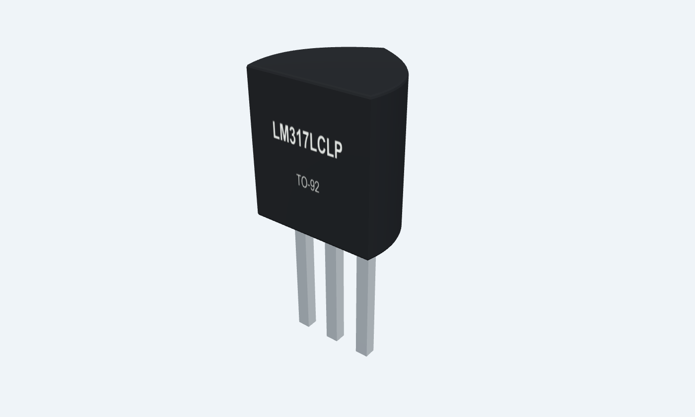
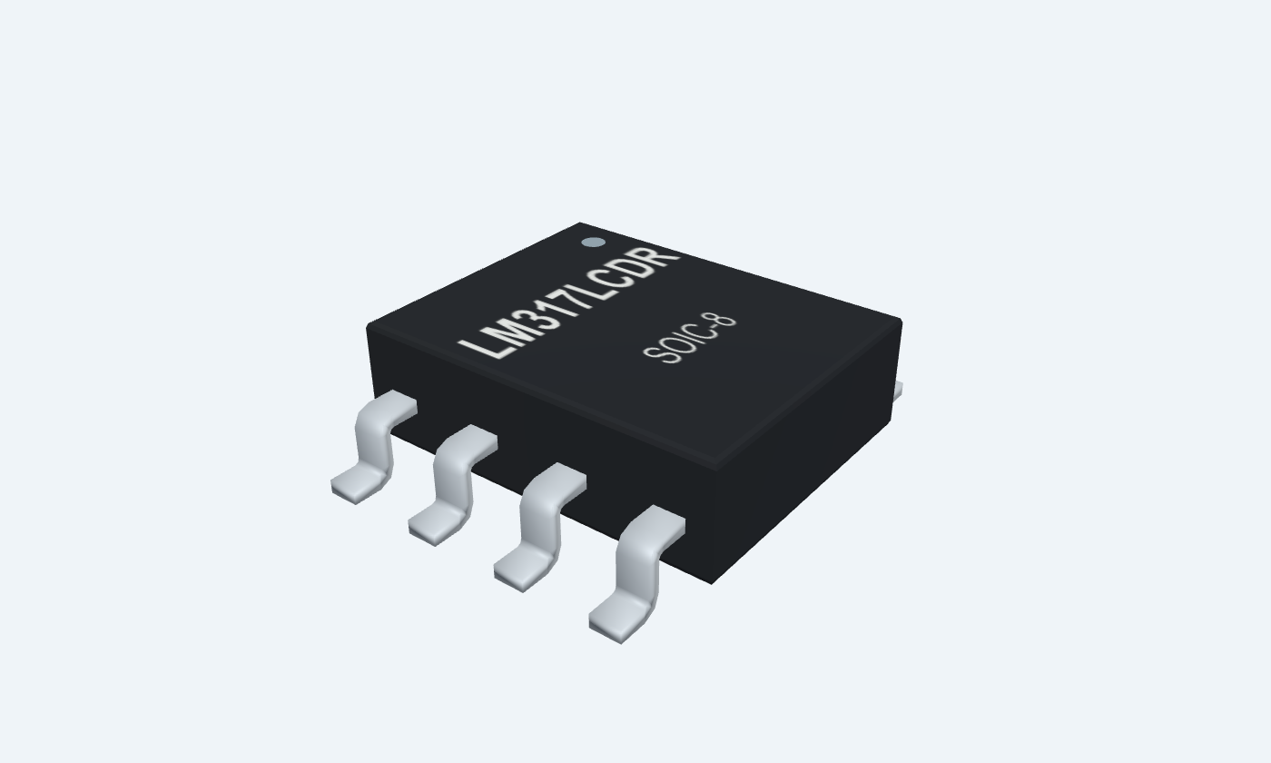
A small adjustable rail with package-aware pin mapping.
LM317L is a low-current adjustable positive linear regulator. Its floating reference and two external resistors set an output near 1.25 V or above, while the series pass stage supplies up to 100 mA under the applicable differential-voltage and thermal conditions. The three-lead TO-92 and eight-lead SOIC have different physical layouts. TO-92 uses INPUT 1, OUTPUT 2 and ADJUST 3; SOIC uses INPUT 1, ADJUST 4 and four internally connected OUTPUT pins, 2, 3, 6 and 7. The package switch updates every view and the footprint. TI SLCS144G distinguishes legacy SHE/TID chips from the new RFB chip. TO-92 remains legacy-only. The tables retain these distinctions rather than assigning the newer 45 V stress limit to every part. A 9 V input, 220 Ω / 660 Ω divider and 500 Ω load illustrate a modest near-5 V supply.
Select a pin to explore its connection
Click a lead or use the arrow keys. Front view · flat face toward you · left-to-right 3 ADJ, 2 OUT, 1 IN
Feeds the series pass regulator.
Connect to the example +9 V supply with local 0.1 µF bypass.
TO-92 and SOIC physical pin 1. Verify chip-origin differential limits.
Supplies the load and resistor divider.
Connect all SOIC OUTPUT leads together on the PCB.
TO-92 pin 2; SOIC pins 2, 3, 6 and 7 are internally common.
Feedback reference, approximately 1.25 V below OUTPUT for legacy chips.
Connect R1 from OUTPUT to ADJUST and R2 from ADJUST to ground.
TO-92 pin 3; SOIC pin 4. ADJUST is not ground.
SOIC pin 3 connects internally to the other OUTPUT pins.
Join all OUTPUT contacts on the PCB.
SOIC only; no corresponding TO-92 lead.
SOIC pin 5 has no internal connection.
May be grounded for improved thermal performance per TI; not required.
SOIC only; no corresponding TO-92 lead.
SOIC pin 6 connects internally to the other OUTPUT pins.
Join all OUTPUT contacts on the PCB.
SOIC only; no corresponding TO-92 lead.
SOIC pin 7 connects internally to the other OUTPUT pins.
Join all OUTPUT contacts on the PCB.
SOIC only; no corresponding TO-92 lead.
SOIC pin 8 has no internal connection.
May be grounded for improved thermal performance per TI; not required.
SOIC only; no corresponding TO-92 lead.
OUTPUT follows ADJUST plus the internal reference. The feedback divider sets output voltage and provides a defined minimum load.
LM317LCLP · TO-92
| Property | Details |
|---|---|
| Manufacturer | Texas Instruments |
| Part number | LM317LCLP |
| Package | TO-92 |
| Connections | 3 pins |
| Mounting | Through-hole |
| Lead pitch | 1.27 mm · straight leads |
| Package code | LP |
| Thermal reference | Legacy chip only; θJA 139.5 or 156.7°C/W under TI conditions |
TI SLCS144G distinctions
Scroll sideways to see all columns.
| Parameter | Value | Conditions / notes |
|---|---|---|
| TO-92 | LM317LCLP · LP0003A | Legacy SHE or TID chip; no new RFB die |
| SOIC-8 | LM317LCDR · D0008A | Legacy SHE/TID or new RFB; verify ordered device |
| TO-92 physical pins | 1 INPUT; 2 OUTPUT; 3 ADJUST | Front view left-to-right: 3,2,1 |
| SOIC physical pins | IN1; OUT2,3,6,7; ADJ4; NC5,8 | All four OUTPUT terminals are internally connected |
| Chip origin | CSO: SHE / TID / RFB | Check manufacturer traceability; package alone is insufficient |
No specifications match. Try a parameter name or a unit.
Package-specific pin maps are explicit. Do not assume another manufacturer uses the same lead order.
SHE / TID / RFB are distinct chip variants
Scroll sideways to see all columns.
| Parameter | Value | Conditions / notes |
|---|---|---|
| Output voltage | SHE 1.25–32 V; TID/RFB 1.25–37 V | With adequate headroom and load |
| Recommended differential | SHE 2.5–32 V; TID/RFB 2.5–37 V | VI−VO |
| Absolute differential | SHE 35 V; TID 40 V; RFB 45 V | Stress limits, not operating targets |
| Recommended output current | 2.5–100 mA | Minimum-load row may require 5 mA for legacy TID |
| LM317LC junction | SHE 0–125°C; TID/RFB −40–125°C | Verify chip origin |
| LM317LI junction | −40–125°C | Industrial grade |
| Absolute junction maximum | 150°C | Recommended operating maximum remains 125°C |
No specifications match. Try a parameter name or a unit.
Never apply the RFB 45 V stress rating to unverified legacy stock.
VI−VO 5–35 V; IO 2.5–100 mA; rated dissipation
Scroll sideways to see all columns.
| Parameter | Value | Conditions / notes |
|---|---|---|
| Legacy VREF min / typ / max | 1.20 / 1.25 / 1.30 V | SHE and TID |
| RFB VREF min / typ / max | 1.220 / 1.256 / 1.292 V | New chip |
| Legacy IADJ | 50 µA typical; 100 µA max. | Flows out of ADJUST |
| RFB IADJ | 44 µA typical; 57 µA max. | New chip |
| Legacy ΔIADJ | 0.2 µA typical; 5 µA max. | 2.5–35 V differential |
| RFB ΔIADJ | 0.8 µA typical; 2.5 µA max. | 2.8–35 V differential |
No specifications match. Try a parameter name or a unit.
Typical values are illustrative; reference and resistor tolerances affect the actual rail.
Manufacturer test conditions retained
Scroll sideways to see all columns.
| Parameter | Value | Conditions / notes |
|---|---|---|
| Legacy line regulation at 25°C | 0.01 typical / 0.02 max. %/V | 5–35 V differential |
| RFB line regulation at 25°C | 0.007 typical / 0.021 max. %/V | 5–35 V differential |
| Legacy line regulation over specified range | 0.02 typical / 0.05 max. %/V | IO 2.5–100 mA |
| RFB line regulation over specified range | 0.006 typical / 0.0275 max. %/V | IO 2.5–100 mA |
| Legacy load regulation, VO≤5 V | 25 mV at 25°C; 50 mV over range | Maximum; IO 2.5–100 mA; 5–35 V differential |
| RFB load regulation, VO≤5 V | 25 mV maximum | At 25°C and over range; same test conditions |
| Ripple with 10 µF CADJ | Legacy 66 min / 80 typ dB; RFB 64 min / 71.5 typ dB | VO10 V; 120 Hz |
| Noise | 10 µV/V typical | 10 Hz–10 kHz; 25°C |
No specifications match. Try a parameter name or a unit.
Avoid mixing new-chip headline numbers with the legacy package specification.
Guaranteed regulation requires the applicable load
Scroll sideways to see all columns.
| Parameter | Value | Conditions / notes |
|---|---|---|
| Minimum load at 35 V differential | SHE 1.5 typ / 2.5 max. mA | Legacy chip |
| Minimum load at 35 V differential | TID 3.5 typ / 5 max. mA | Legacy chip |
| Minimum load at 35 V differential | RFB 1.28 typ / 1.72 max. mA | Recommended operating floor is still 2.5 mA |
| Legacy SHE peak current | 100 mA minimum; 200 mA typical | Differential ≤35 V |
| Legacy TID peak current | 100 min / 200 typ mA at 3–13 V | At 35 V: 25 min / 50 typ / 150 max. mA |
| New RFB peak current | 160 min / 290 typ mA | Differential ≤35 V; not a 290 mA continuous rating |
| Example divider minimum | 1.20 / 222.2 ≈5.40 mA | 220 Ω at +1%; covers 5 mA legacy requirement |
No specifications match. Try a parameter name or a unit.
Thermal limits apply in addition to current limiting.
Board-dependent thermal figures
Scroll sideways to see all columns.
| Parameter | Value | Conditions / notes |
|---|---|---|
| TO-92 θJA | 139.5 SHE / 156.7 TID °C/W | Manufacturer reference conditions |
| SOIC θJA | 97.1 SHE / 96.5 TID / 98.18 RFB °C/W | Actual PCB and airflow change the result |
| Local input bypass | 0.1 µF | Especially with long supply wiring |
| Output capacitor | 1 µF optional for transient response | No output capacitor required for stability per TI |
| Adjustment bypass | Optional 10 µF | Review protection diodes when adding stored charge |
| Example pass loss | ≈62.7 mW | (9−5) × (5/500+1.25/220) |
No specifications match. Try a parameter name or a unit.
Protection is not a substitute for correct operating voltage, minimum load or thermal design.
220 Ω / 660 Ω · 500 Ω load
Scroll sideways to see all columns.
| Parameter | Value | Conditions / notes |
|---|---|---|
| Input / bypass | 9 V / 0.1 µF | Common ground return |
| Ideal legacy output | 1.25 × (1+660/220) = 5.00 V | Before adjustment current |
| Legacy typical corrected output | 5.033 V | Adds 50 µA × 660 Ω |
| New RFB typical corrected output | 5.05304 V | 1.256 ×4 +44 µA ×660 |
| Load / divider current | 10 mA / 5.682 mA | Nominal 5 V legacy calculation |
| Resistor power | 50 mW in 500 Ω load | Use 0.25 W or higher appropriately rated resistors |
| Output capacitor | 1 µF, suitably rated | Follow manufacturer bypass/protection guidance |
No specifications match. Try a parameter name or a unit.
Calculated illustration, not a measured or time-domain simulation.
Select a pin for its function, connection guidance and electrical notes.
Follow the labeled connections and functional stages
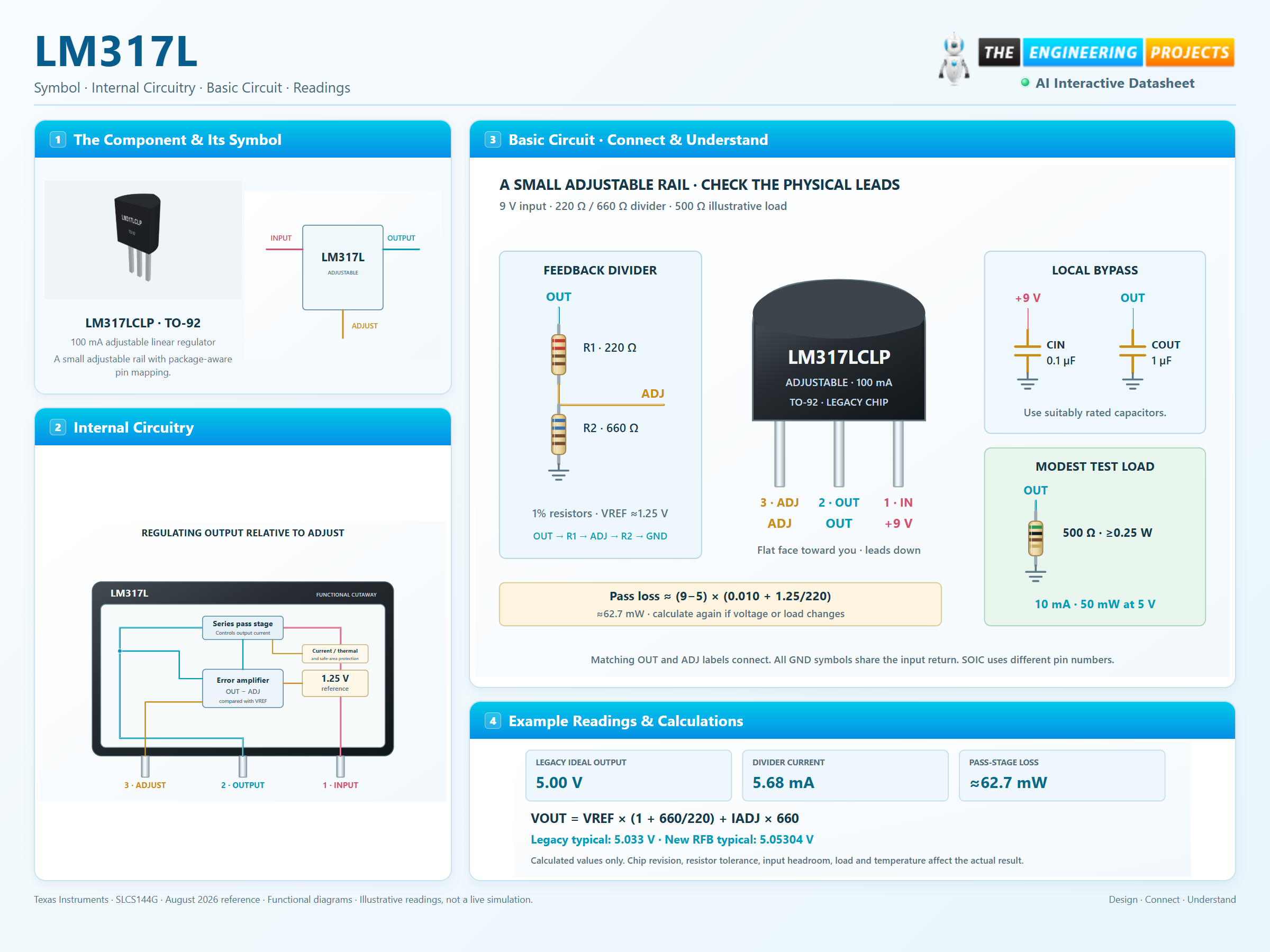
3 stages · Explore one step at a time
TO-92 front-view order is ADJ3, OUT2, IN1. On SOIC, connect all four output contacts.
220 Ω runs from OUT to ADJ and 660 Ω from ADJ to ground. A 500 Ω load draws nominally 10 mA.
Read the source chip-origin conditions. A 9-to-5 V example dissipates about 63 mW in the pass stage before small corrections.
TO-92 regulator with named electrical nets and a defined load.
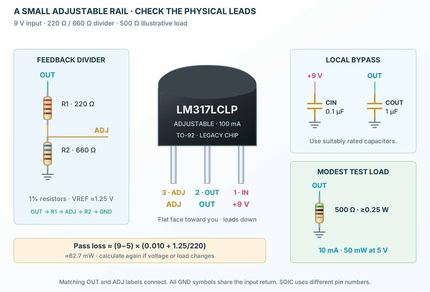
Follow the component values and pin connections
Supply INPUT1 from 9 V and share all ground returns.
220 Ω from OUT2 to ADJ3 and 660 Ω to ground set the voltage.
A 500 Ω load draws approximately 10 mA; the divider adds 5.68 mA.
A floating reference and pass stage inside a compact IC outline.
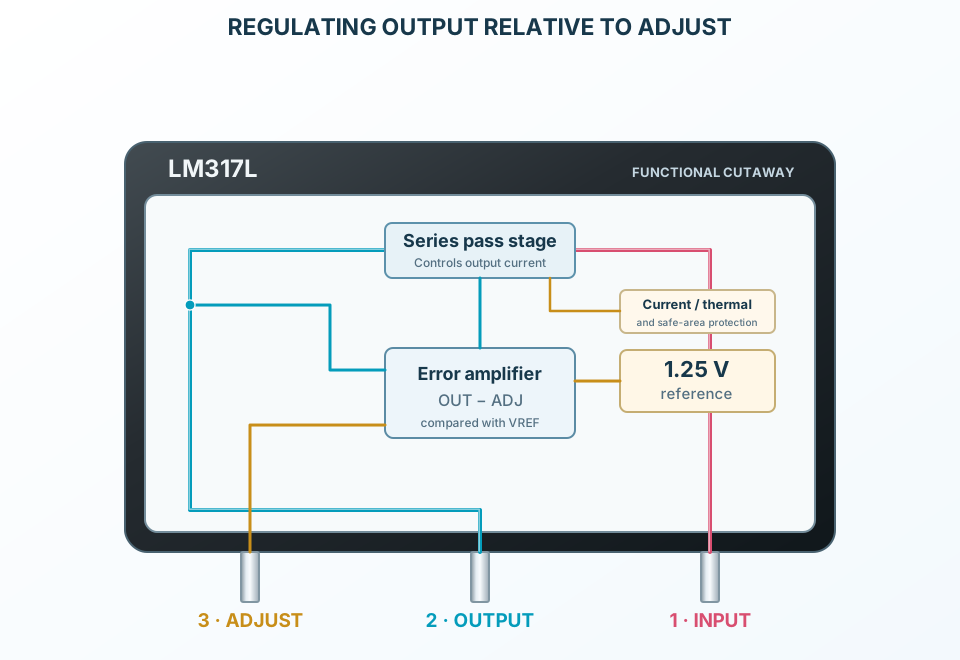
Select a stage to see its role and connections
Compare OUTPUT minus ADJUST with the internal reference.
Drive the series pass stage to correct the voltage error.
Current and thermal controls constrain overloads.
Signal names, electrical functions and connection guidance
Scroll within the table to see all columns and rows.
| Pin | Signal | Type | Function & connection |
|---|---|---|---|
| INPUT | Supply input | Feeds the series pass regulator.Connection guidanceConnect to the example +9 V supply with local 0.1 µF bypass. TO-92 and SOIC physical pin 1. Verify chip-origin differential limits. | |
| OUTPUT | Regulated output | Supplies the load and resistor divider.Connection guidanceConnect all SOIC OUTPUT leads together on the PCB. TO-92 pin 2; SOIC pins 2, 3, 6 and 7 are internally common. | |
| ADJUST | Adjustment terminal | Feedback reference, approximately 1.25 V below OUTPUT for legacy chips.Connection guidanceConnect R1 from OUTPUT to ADJUST and R2 from ADJUST to ground. TO-92 pin 3; SOIC pin 4. ADJUST is not ground. | |
| OUTPUT | Common output contact | SOIC pin 3 connects internally to the other OUTPUT pins.Connection guidanceJoin all OUTPUT contacts on the PCB. SOIC only; no corresponding TO-92 lead. | |
| NC | No internal connection | SOIC pin 5 has no internal connection.Connection guidanceMay be grounded for improved thermal performance per TI; not required. SOIC only; no corresponding TO-92 lead. | |
| OUTPUT | Common output contact | SOIC pin 6 connects internally to the other OUTPUT pins.Connection guidanceJoin all OUTPUT contacts on the PCB. SOIC only; no corresponding TO-92 lead. | |
| OUTPUT | Common output contact | SOIC pin 7 connects internally to the other OUTPUT pins.Connection guidanceJoin all OUTPUT contacts on the PCB. SOIC only; no corresponding TO-92 lead. | |
| NC | No internal connection | SOIC pin 8 has no internal connection.Connection guidanceMay be grounded for improved thermal performance per TI; not required. SOIC only; no corresponding TO-92 lead. |
No pins match these filters. Try another signal name or reset the filters.
TI SLCS144G distinctions
Scroll within the table to see all columns and rows.
| Parameter | Value | Conditions / notes |
|---|---|---|
| TO-92 | LM317LCLP · LP0003A | Legacy SHE or TID chip; no new RFB die |
| SOIC-8 | LM317LCDR · D0008A | Legacy SHE/TID or new RFB; verify ordered device |
| TO-92 physical pins | 1 INPUT; 2 OUTPUT; 3 ADJUST | Front view left-to-right: 3,2,1 |
| SOIC physical pins | IN1; OUT2,3,6,7; ADJ4; NC5,8 | All four OUTPUT terminals are internally connected |
| Chip origin | CSO: SHE / TID / RFB | Check manufacturer traceability; package alone is insufficient |
No specifications match. Try a parameter name or a unit.
Package-specific pin maps are explicit. Do not assume another manufacturer uses the same lead order.
SHE / TID / RFB are distinct chip variants
Scroll within the table to see all columns and rows.
| Parameter | Value | Conditions / notes |
|---|---|---|
| Output voltage | SHE 1.25–32 V; TID/RFB 1.25–37 V | With adequate headroom and load |
| Recommended differential | SHE 2.5–32 V; TID/RFB 2.5–37 V | VI−VO |
| Absolute differential | SHE 35 V; TID 40 V; RFB 45 V | Stress limits, not operating targets |
| Recommended output current | 2.5–100 mA | Minimum-load row may require 5 mA for legacy TID |
| LM317LC junction | SHE 0–125°C; TID/RFB −40–125°C | Verify chip origin |
| LM317LI junction | −40–125°C | Industrial grade |
| Absolute junction maximum | 150°C | Recommended operating maximum remains 125°C |
No specifications match. Try a parameter name or a unit.
Never apply the RFB 45 V stress rating to unverified legacy stock.
VI−VO 5–35 V; IO 2.5–100 mA; rated dissipation
Scroll within the table to see all columns and rows.
| Parameter | Value | Conditions / notes |
|---|---|---|
| Legacy VREF min / typ / max | 1.20 / 1.25 / 1.30 V | SHE and TID |
| RFB VREF min / typ / max | 1.220 / 1.256 / 1.292 V | New chip |
| Legacy IADJ | 50 µA typical; 100 µA max. | Flows out of ADJUST |
| RFB IADJ | 44 µA typical; 57 µA max. | New chip |
| Legacy ΔIADJ | 0.2 µA typical; 5 µA max. | 2.5–35 V differential |
| RFB ΔIADJ | 0.8 µA typical; 2.5 µA max. | 2.8–35 V differential |
No specifications match. Try a parameter name or a unit.
Typical values are illustrative; reference and resistor tolerances affect the actual rail.
Manufacturer test conditions retained
Scroll within the table to see all columns and rows.
| Parameter | Value | Conditions / notes |
|---|---|---|
| Legacy line regulation at 25°C | 0.01 typical / 0.02 max. %/V | 5–35 V differential |
| RFB line regulation at 25°C | 0.007 typical / 0.021 max. %/V | 5–35 V differential |
| Legacy line regulation over specified range | 0.02 typical / 0.05 max. %/V | IO 2.5–100 mA |
| RFB line regulation over specified range | 0.006 typical / 0.0275 max. %/V | IO 2.5–100 mA |
| Legacy load regulation, VO≤5 V | 25 mV at 25°C; 50 mV over range | Maximum; IO 2.5–100 mA; 5–35 V differential |
| RFB load regulation, VO≤5 V | 25 mV maximum | At 25°C and over range; same test conditions |
| Ripple with 10 µF CADJ | Legacy 66 min / 80 typ dB; RFB 64 min / 71.5 typ dB | VO10 V; 120 Hz |
| Noise | 10 µV/V typical | 10 Hz–10 kHz; 25°C |
No specifications match. Try a parameter name or a unit.
Avoid mixing new-chip headline numbers with the legacy package specification.
Guaranteed regulation requires the applicable load
Scroll within the table to see all columns and rows.
| Parameter | Value | Conditions / notes |
|---|---|---|
| Minimum load at 35 V differential | SHE 1.5 typ / 2.5 max. mA | Legacy chip |
| Minimum load at 35 V differential | TID 3.5 typ / 5 max. mA | Legacy chip |
| Minimum load at 35 V differential | RFB 1.28 typ / 1.72 max. mA | Recommended operating floor is still 2.5 mA |
| Legacy SHE peak current | 100 mA minimum; 200 mA typical | Differential ≤35 V |
| Legacy TID peak current | 100 min / 200 typ mA at 3–13 V | At 35 V: 25 min / 50 typ / 150 max. mA |
| New RFB peak current | 160 min / 290 typ mA | Differential ≤35 V; not a 290 mA continuous rating |
| Example divider minimum | 1.20 / 222.2 ≈5.40 mA | 220 Ω at +1%; covers 5 mA legacy requirement |
No specifications match. Try a parameter name or a unit.
Thermal limits apply in addition to current limiting.
Board-dependent thermal figures
Scroll within the table to see all columns and rows.
| Parameter | Value | Conditions / notes |
|---|---|---|
| TO-92 θJA | 139.5 SHE / 156.7 TID °C/W | Manufacturer reference conditions |
| SOIC θJA | 97.1 SHE / 96.5 TID / 98.18 RFB °C/W | Actual PCB and airflow change the result |
| Local input bypass | 0.1 µF | Especially with long supply wiring |
| Output capacitor | 1 µF optional for transient response | No output capacitor required for stability per TI |
| Adjustment bypass | Optional 10 µF | Review protection diodes when adding stored charge |
| Example pass loss | ≈62.7 mW | (9−5) × (5/500+1.25/220) |
No specifications match. Try a parameter name or a unit.
Protection is not a substitute for correct operating voltage, minimum load or thermal design.
220 Ω / 660 Ω · 500 Ω load
Scroll within the table to see all columns and rows.
| Parameter | Value | Conditions / notes |
|---|---|---|
| Input / bypass | 9 V / 0.1 µF | Common ground return |
| Ideal legacy output | 1.25 × (1+660/220) = 5.00 V | Before adjustment current |
| Legacy typical corrected output | 5.033 V | Adds 50 µA × 660 Ω |
| New RFB typical corrected output | 5.05304 V | 1.256 ×4 +44 µA ×660 |
| Load / divider current | 10 mA / 5.682 mA | Nominal 5 V legacy calculation |
| Resistor power | 50 mW in 500 Ω load | Use 0.25 W or higher appropriately rated resistors |
| Output capacitor | 1 µF, suitably rated | Follow manufacturer bypass/protection guidance |
No specifications match. Try a parameter name or a unit.
Calculated illustration, not a measured or time-domain simulation.
No matching rowsTry a pin name, parameter, unit or test condition, or reset the filters.
Power modest analog or bias loads when voltage drop and heat are acceptable.
Manufacturer application guideExplore divider tolerance, adjustment current and minimum load.
Manufacturer application guideUse the manufacturer current-source topology within current and compliance limits.
Manufacturer application guideFind LM317L in the Components Library to place its schematic symbol and connect its pins.
Reference page · circuit simulation model not yet availableOpen ProTech