LM331Voltage-to-frequency converter
Measure an analog voltage by counting its output pulses.
LM331 converts an analog voltage into a train of pulses whose frequency can be counted digitally. Its reference current source, comparator and timed switching circuit balance charge in an external integration network. Properly chosen components allow accurate conversion without a conventional parallel ADC interface. The example follows the manufacturer’s stand-alone voltage-to-frequency circuit with a15V analog supply and a5V output pull-up. A gain trimmer calibrates the nominal10V-to10kHz scale. The internal current output and the open-collector frequency output have different jobs and must be wired separately. This page covers TI LM331N/NOPB in its documented PDIP-8 package. No unverified SMD substitute is presented as the same TI device. Use stable resistors and low-absorption capacitors, calibrate the gain, and allow the input filter and integration network to settle before interpreting the pulse rate.
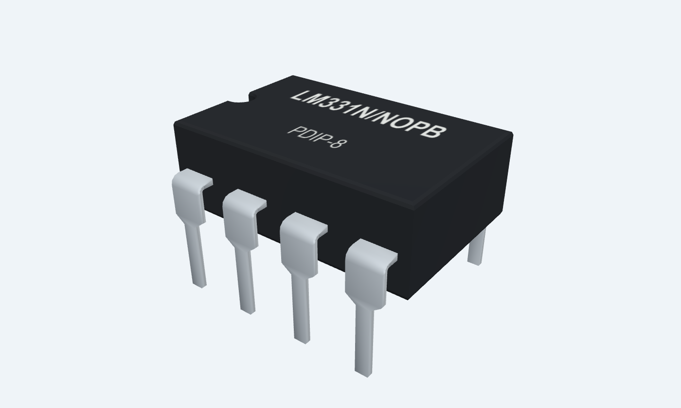

8Physical pins
LM331N/NOPBPDIP-8
Manufacturer-referencedTexas Instruments
Pin diagram
Select a pin to explore its connection
Highlight
LM331PDIP-8Top view
Click a lead or use the arrow keys. Top view
PIN 1 · Current and frequency outputs
Switched current sourceIOUT
Function
Delivers reference-controlled charge pulses to the integration network.
How to connect
Join THRESH6 at the RL/CL top node.
Electrical note
Not the logic frequency output.
PIN 2 · Reference current
Reference current settingIREF
Function
Approximately1.89V at the current-setting contact.
How to connect
Connect12kΩ plus5kΩ gain-adjust rheostat in series toGND.
Electrical note
Tie rheostat wiper to its unused end for reliable adjustment.
PIN 3 · Current and frequency outputs
Open-collector pulse outputFOUT
Function
Outputs a pulse train whose frequency follows the input.
How to connect
Pull up through10kΩ to+5V; connect a frequency counter.
Electrical note
Requires a pull-up; do not assume a push-pull HIGH.
PIN 4 · Ground
Supply returnGND
Function
Common analog and logic reference.
How to connect
Connect all ground symbols here.
PIN 5 · Timing network
Timing nodeRC
Function
Charges toward the internal timer threshold and then resets.
How to connect
Connect6.8kΩ to+15V and10nF toGND.
Electrical note
Use stable, low-leakage timing parts.
PIN 6 · Comparator inputs
Comparator thresholdTHRESH
Function
Monitors the integrated feedback voltage.
How to connect
Join IOUT1; RL100kΩ and CL1µF in parallel connect to the47Ω return node.
PIN 7 · Comparator inputs
Comparator signal inputCOMPIN
Function
Receives the filtered voltage to convert.
How to connect
Apply VIN through100kΩ; bypass this pin toGND with100nF.
Electrical note
Keep normal input below VS−2V.
PIN 8 · Supply
Positive supplyVS
Function
Powers the converter.
How to connect
Apply+15V in this example; bypass locally with100nF.
Electrical note
Recommended device supply4–40V; circuit limits also matter.
Key specifications
Measure an analog voltage by counting its output pulses.
Recommended supply4–40 V
Example calibrated scale1 kHz per volt
Operating ambient0–70 °C
Typical supply current3 mA at5V
Package details
LM331N/NOPB · PDIP-8
| Property | Details |
|---|---|
| Manufacturer | Texas Instruments |
| Part number | LM331N/NOPB |
| Package | PDIP-8 |
| Connections | 8 pins |
| Mounting | Through-hole |
| Lead pitch | 2.54 mm |
| Package code | PDIP-8 |
| Thermal reference | See operating and package limits |
Operating conditions
TI LM331 commercial grade
Manufacturer specifications 6 parameters
Scroll sideways to see all columns.
| Parameter | Value | Conditions / notes |
|---|---|---|
| Supply | 4–40V | 15V in the example |
| Ambient | 0–70°C | LM331; LM231 grade differs |
| Comparator common-mode range | −0.2V toVS−2V | Over rated temperature |
| Supply current at5V | 3mA typical;6mA max | LM331, stated test circuit |
| Supply current at40V | 4mA typical;8mA max | Stated test circuit |
| Full-scale frequency capability | 1Hz to100kHz feature range | Requires an appropriate application circuit |
No specifications match. Try a parameter name or a unit.
The shown circuit is calibrated for10kHz full scale, not automatically for100kHz.
Accuracy and calibration
Keep the test circuit distinction
Manufacturer specifications 6 parameters
Scroll sideways to see all columns.
| Parameter | Value | Conditions / notes |
|---|---|---|
| Figure16 precision circuit nonlinearity | ±0.003% typical;±0.01% max | 4.5–20V,25°C, stated calibrated conditions |
| Shown Figure14 circuit nonlinearity | ±0.024% typical;±0.14% max | 15V;10Hz to11kHz |
| Untrimmed LM331 scale factor | 0.9–1.1kHz/V | Figure16 conditions;RS14kΩ |
| Gain temperature drift | ±30ppm/°C typical;±150ppm/°C max | Non-A LM331;4.5–20V |
| Comparator offset | ±3mV typical;±10mV max | 25°C |
| Comparator bias current | −80nA typical;−300nA max | Stated conditions |
No specifications match. Try a parameter name or a unit.
The precision-circuit headline is not the guaranteed accuracy of this simpler stand-alone example.
Reference and output
25°C unless stated
Manufacturer specifications 6 parameters
Scroll sideways to see all columns.
| Parameter | Value | Conditions / notes |
|---|---|---|
| IREF voltage | 1.89V typical;1.70–2.08V | LM331 |
| Switched IOUT | 136µA typical;116–156µA | RS14kΩ;IOUT at0V |
| Timer threshold | 0.667VS typical;0.63–0.70VS | RC pin5 |
| FOUT LOW | 0.15V typical;0.5V max | Sinking5mA |
| FOUT LOW overtemperature | 0.1V typical;0.4V max | Sinking3.2mA |
| FOUT OFF leakage | ±0.05µA typical;1µA max | Open collector |
No specifications match. Try a parameter name or a unit.
No load should force output or input terminals beyond their specified limits.
Stand-alone conversion network
Adapted from TI Figure14
Manufacturer specifications 8 parameters
Scroll sideways to see all columns.
| Parameter | Value | Conditions / notes |
|---|---|---|
| Analog supply / output pull-up | 15V /5V | 100nF local supply bypass;FOUT through10kΩ to5V |
| RT / CT | 6.8kΩ /10nF | RT from15V toRC5;CT fromRC5 toGND |
| RIN / CIN | 100kΩ /100nF | VIN throughRIN toCOMPIN7;CIN toGND |
| RL / CL | 100kΩ /1µF in parallel | From joinedIOUT1/THRESH6 toRETURN |
| Hysteresis return | 47Ω fromRETURN toGND | Shared lower end ofRL andCL |
| RS | 12kΩ plus5kΩ rheostat | IREF2 toGND; trim gain |
| Logic output | FOUT3 tofrequency counter | Open collector with10kΩ pull-up |
| Offset adjustment | Optional manufacturer network omitted | Gain calibration retained |
No specifications match. Try a parameter name or a unit.
Use a film or other suitable low-absorption integration capacitor and stable timing components. Matching labels identify connected nodes.
Nominal conversion relationships
Ideal charge balance
Manufacturer specifications 6 parameters
Scroll sideways to see all columns.
| Parameter | Value | Conditions / notes |
|---|---|---|
| Frequency | fOUT=(VIN/2.09V)×(RS/RL)×1/(RTCT) | Manufacturer application equation |
| Gain for1kHz/V | RS≈14.212kΩ | RL100kΩ,RT6.8kΩ,CT10nF; then calibrate |
| Timed current pulse | t≈1.1RTCT≈74.8µs | Nominal timing interval |
| Example input | 2.5V→2.5kHz | After calibration |
| Pulse count in100ms | 250 pulses at2.5V | Quantization step≈10mV per count |
| Response time | Filter and integration dependent | Do not treat one pulse as an instant precision reading |
No specifications match. Try a parameter name or a unit.
Values are nominal calculations; device gain, offset and component tolerance require calibration.
Package and thermal reference
LM331N/NOPB · PDIP-8
Manufacturer specifications 7 parameters
Scroll sideways to see all columns.
| Parameter | Value | Conditions / notes |
|---|---|---|
| Pitch | 2.54 mm | Through-hole |
| Verified TI package | 8-pinPDIP(P) | No TI SMD option in the cited orderable table |
| Absolute supply | 40V | Same numerical upper limit as recommended; do not exceed |
| Absolute input | −0.2V toVS | Stress rating |
| Maximum junction | 150°C | Apply thermal derating |
| Junction-to-ambient | 100°C/W | Specified PDIP reference |
| Storage | −65 to+150°C | Unpowered |
No specifications match. Try a parameter name or a unit.
Verify the exact manufacturer and ordering suffix when sourcing parts.
Connections by function
Select a pin for its function, connection guidance and electrical notes.
Current and frequency outputs2 pins
Reference current1 pin
Ground1 pin
Timing network1 pin
Comparator inputs2 pins
Supply1 pin
LM331 at a glance
Follow the labeled connections and functional stages
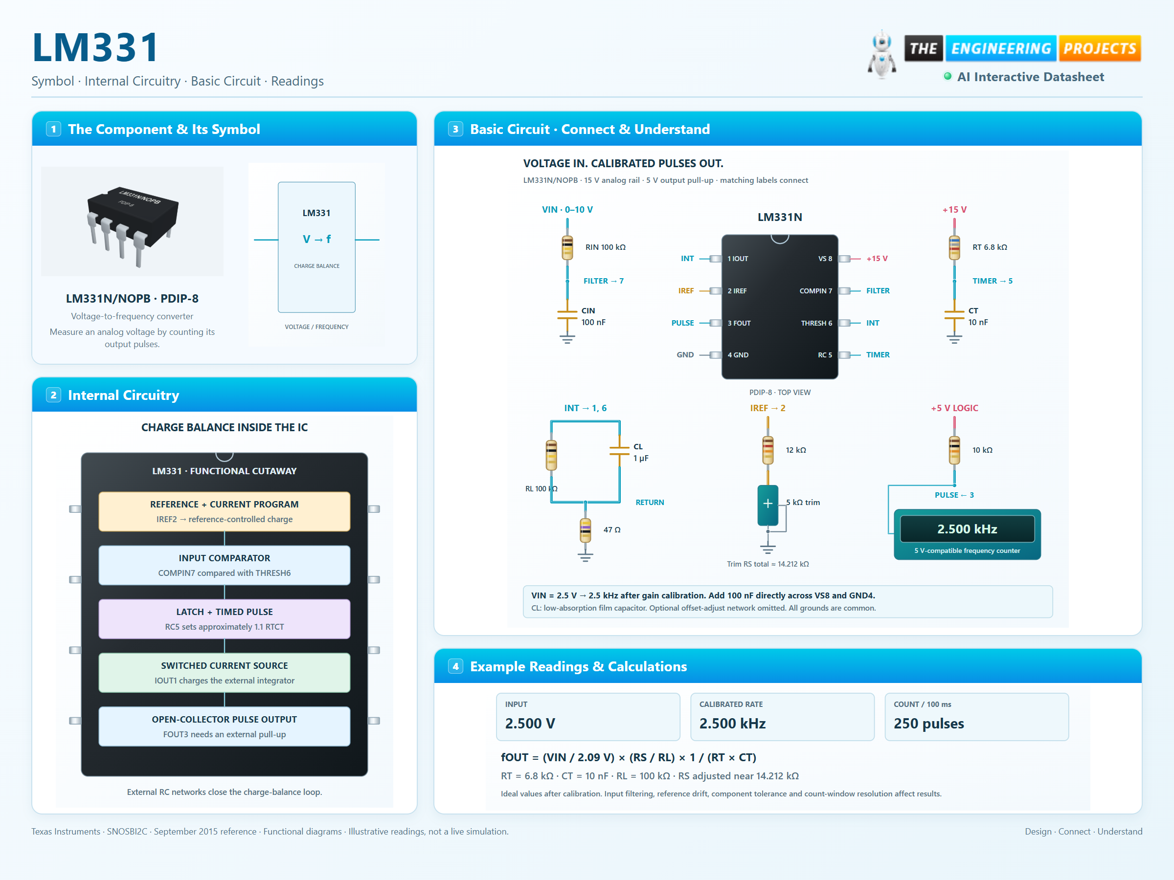
How it works
3 stages · Explore one step at a time
Compare
The comparator compares filtered VIN with the integrated feedback voltage.
Deliver charge
A timed pulse routes reference current into the integration network.
Balance and count
The repetition rate settles so average feedback follows VIN. Count FOUT pulses to recover the input level.
Step 1 of 3
LM331 in a circuit
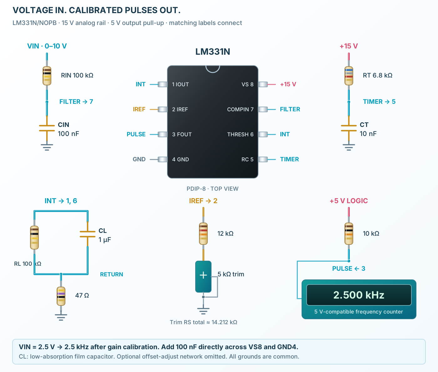
15V analog supply,5V frequency output.
Connect it, step by step
Follow the component values and pin connections
Build the networks
Keep input-filter and integration components close to the IC.
Trim the gain
Apply a known input and adjustRS for the intended output frequency.
Count
Use a5V-compatible counter on FOUT and allow settling.
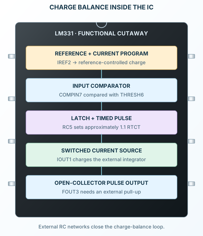
Inside LM331
Reference current, comparator, timer and pulse output.
Explore the circuit
Select a stage to see its role and connections
Reference
IREF controls the switched current.
Timing
RC sets a nominal charge-pulse duration.
Output
FOUT supplies countable open-collector pulses.
Selected packagePDIP-8LM331N/NOPB
Physical connections8 pinsPackage-specific numbering
Reference collection7 tables39 parameters & pin functions
Pin reference
Signal names, electrical functions and connection guidance
Physical pin numbers8 pins
Scroll within the table to see all columns and rows.
| Pin | Signal | Type | Function & connection |
|---|---|---|---|
| IOUT | Switched current source | Delivers reference-controlled charge pulses to the integration network.Connection guidanceJoin THRESH6 at the RL/CL top node. Not the logic frequency output. | |
| IREF | Reference current setting | Approximately1.89V at the current-setting contact.Connection guidanceConnect12kΩ plus5kΩ gain-adjust rheostat in series toGND. Tie rheostat wiper to its unused end for reliable adjustment. | |
| FOUT | Open-collector pulse output | Outputs a pulse train whose frequency follows the input.Connection guidancePull up through10kΩ to+5V; connect a frequency counter. Requires a pull-up; do not assume a push-pull HIGH. | |
| GND | Supply return | Common analog and logic reference.Connection guidanceConnect all ground symbols here. | |
| RC | Timing node | Charges toward the internal timer threshold and then resets.Connection guidanceConnect6.8kΩ to+15V and10nF toGND. Use stable, low-leakage timing parts. | |
| THRESH | Comparator threshold | Monitors the integrated feedback voltage.Connection guidanceJoin IOUT1; RL100kΩ and CL1µF in parallel connect to the47Ω return node. | |
| COMPIN | Comparator signal input | Receives the filtered voltage to convert.Connection guidanceApply VIN through100kΩ; bypass this pin toGND with100nF. Keep normal input below VS−2V. | |
| VS | Positive supply | Powers the converter.Connection guidanceApply+15V in this example; bypass locally with100nF. Recommended device supply4–40V; circuit limits also matter. |
No pins match these filters. Try another signal name or reset the filters.
Operating conditions
TI LM331 commercial grade
Manufacturer-referenced values6 parameters
Scroll within the table to see all columns and rows.
| Parameter | Value | Conditions / notes |
|---|---|---|
| Supply | 4–40V | 15V in the example |
| Ambient | 0–70°C | LM331; LM231 grade differs |
| Comparator common-mode range | −0.2V toVS−2V | Over rated temperature |
| Supply current at5V | 3mA typical;6mA max | LM331, stated test circuit |
| Supply current at40V | 4mA typical;8mA max | Stated test circuit |
| Full-scale frequency capability | 1Hz to100kHz feature range | Requires an appropriate application circuit |
No specifications match. Try a parameter name or a unit.
The shown circuit is calibrated for10kHz full scale, not automatically for100kHz.
Accuracy and calibration
Keep the test circuit distinction
Manufacturer-referenced values6 parameters
Scroll within the table to see all columns and rows.
| Parameter | Value | Conditions / notes |
|---|---|---|
| Figure16 precision circuit nonlinearity | ±0.003% typical;±0.01% max | 4.5–20V,25°C, stated calibrated conditions |
| Shown Figure14 circuit nonlinearity | ±0.024% typical;±0.14% max | 15V;10Hz to11kHz |
| Untrimmed LM331 scale factor | 0.9–1.1kHz/V | Figure16 conditions;RS14kΩ |
| Gain temperature drift | ±30ppm/°C typical;±150ppm/°C max | Non-A LM331;4.5–20V |
| Comparator offset | ±3mV typical;±10mV max | 25°C |
| Comparator bias current | −80nA typical;−300nA max | Stated conditions |
No specifications match. Try a parameter name or a unit.
The precision-circuit headline is not the guaranteed accuracy of this simpler stand-alone example.
Reference and output
25°C unless stated
Manufacturer-referenced values6 parameters
Scroll within the table to see all columns and rows.
| Parameter | Value | Conditions / notes |
|---|---|---|
| IREF voltage | 1.89V typical;1.70–2.08V | LM331 |
| Switched IOUT | 136µA typical;116–156µA | RS14kΩ;IOUT at0V |
| Timer threshold | 0.667VS typical;0.63–0.70VS | RC pin5 |
| FOUT LOW | 0.15V typical;0.5V max | Sinking5mA |
| FOUT LOW overtemperature | 0.1V typical;0.4V max | Sinking3.2mA |
| FOUT OFF leakage | ±0.05µA typical;1µA max | Open collector |
No specifications match. Try a parameter name or a unit.
No load should force output or input terminals beyond their specified limits.
Stand-alone conversion network
Adapted from TI Figure14
Manufacturer-referenced values8 parameters
Scroll within the table to see all columns and rows.
| Parameter | Value | Conditions / notes |
|---|---|---|
| Analog supply / output pull-up | 15V /5V | 100nF local supply bypass;FOUT through10kΩ to5V |
| RT / CT | 6.8kΩ /10nF | RT from15V toRC5;CT fromRC5 toGND |
| RIN / CIN | 100kΩ /100nF | VIN throughRIN toCOMPIN7;CIN toGND |
| RL / CL | 100kΩ /1µF in parallel | From joinedIOUT1/THRESH6 toRETURN |
| Hysteresis return | 47Ω fromRETURN toGND | Shared lower end ofRL andCL |
| RS | 12kΩ plus5kΩ rheostat | IREF2 toGND; trim gain |
| Logic output | FOUT3 tofrequency counter | Open collector with10kΩ pull-up |
| Offset adjustment | Optional manufacturer network omitted | Gain calibration retained |
No specifications match. Try a parameter name or a unit.
Use a film or other suitable low-absorption integration capacitor and stable timing components. Matching labels identify connected nodes.
Nominal conversion relationships
Ideal charge balance
Manufacturer-referenced values6 parameters
Scroll within the table to see all columns and rows.
| Parameter | Value | Conditions / notes |
|---|---|---|
| Frequency | fOUT=(VIN/2.09V)×(RS/RL)×1/(RTCT) | Manufacturer application equation |
| Gain for1kHz/V | RS≈14.212kΩ | RL100kΩ,RT6.8kΩ,CT10nF; then calibrate |
| Timed current pulse | t≈1.1RTCT≈74.8µs | Nominal timing interval |
| Example input | 2.5V→2.5kHz | After calibration |
| Pulse count in100ms | 250 pulses at2.5V | Quantization step≈10mV per count |
| Response time | Filter and integration dependent | Do not treat one pulse as an instant precision reading |
No specifications match. Try a parameter name or a unit.
Values are nominal calculations; device gain, offset and component tolerance require calibration.
Package and thermal reference
LM331N/NOPB · PDIP-8
Manufacturer-referenced values7 parameters
Scroll within the table to see all columns and rows.
| Parameter | Value | Conditions / notes |
|---|---|---|
| Pitch | 2.54 mm | Through-hole |
| Verified TI package | 8-pinPDIP(P) | No TI SMD option in the cited orderable table |
| Absolute supply | 40V | Same numerical upper limit as recommended; do not exceed |
| Absolute input | −0.2V toVS | Stress rating |
| Maximum junction | 150°C | Apply thermal derating |
| Junction-to-ambient | 100°C/W | Specified PDIP reference |
| Storage | −65 to+150°C | Unpowered |
No specifications match. Try a parameter name or a unit.
Verify the exact manufacturer and ordering suffix when sourcing parts.
No matching rowsTry a pin name, parameter, unit or test condition, or reset the filters.
Remote measurements
Transmit a frequency signal after suitable buffering or isolation.
Manufacturer application guideLow-cost conversion
Use a digital counter to measure conditioned analog levels.
Manufacturer application guideFrequency-to-voltage conversion
A different manufacturer application circuit reverses the conversion; the wiring differs from this example.
Manufacturer application guideTake it into ProTech
Find LM331 in the Components Library to place its schematic symbol and connect its pins.
Reference page · circuit simulation model not yet availableOpen ProTech