Real View
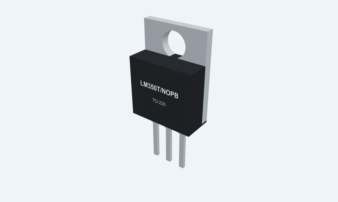
Set the voltage with two resistors—and design the thermal path.
LM350 is a three-terminal adjustable positive linear regulator in the 3 A class. Its floating control loop maintains approximately 1.25 V between OUTPUT and ADJUST, and two resistors translate that reference into the desired output voltage. The nominal adjustment range is 1.2–33 V when input headroom, minimum load and thermal requirements are satisfied. Excess input voltage becomes heat in the series pass stage; a 3 A current capability does not mean the bare package can continuously dissipate the resulting power. This page follows the standard TI LM350 column in SNVS772B and the LM350T/NOPB TO-220 package. The front-view leads are ADJUST, OUTPUT and INPUT, and the metal tab is OUTPUT. A 9 V-to-5 V example uses a 110 Ω / 330 Ω divider, a 50 Ω load and local bypass capacitors to show regulation, minimum-load margin and dissipation together.
Select a pin to explore its connection
Click a lead or use the arrow keys. Front view · marking toward you · ADJ1, OUT2, IN3
The loop regulates OUTPUT approximately 1.25 V above ADJUST.
Connect the junction of R1 from OUTPUT and R2 to the return.
This is not ground; adjustment-pin current contributes IADJ × R2 to output voltage.
Supplies the external load and feedback divider. The metal tab is electrically connected to OUTPUT.
Connect R1 close to this lead and return R2 near the load return.
A grounded heatsink needs appropriate electrical insulation from the live output tab.
Powers the series pass stage.
Use +9 V in the example, with a local 0.1 µF bypass to the common return.
Keep adequate headroom. The 35 V stress limit is input-to-output differential.
The loop holds OUT minus ADJ near 1.25 V. R1 carries a nearly constant current and R2 lifts the adjustment pin above ground, setting the output.
LM350T/NOPB · TO-220
| Property | Details |
|---|---|
| Manufacturer | Texas Instruments |
| Part number | LM350T/NOPB |
| Package | TO-220 |
| Connections | 3 pins |
| Mounting | Through-hole |
| Lead pitch | 2.54 mm |
| Package code | NDE |
| Thermal reference | Output tab; use a suitable thermal path |
Standard LM350 · not LM350A
Scroll sideways to see all columns.
| Parameter | Value | Conditions / notes |
|---|---|---|
| Nominal adjustable output | 1.2–33 V | With sufficient input headroom and load |
| Operating junction temperature | 0–125°C | This is junction, not ambient temperature |
| Reference voltage | 1.20 / 1.25 / 1.30 V | Minimum / typical / maximum; stated electrical conditions |
| Adjustment-pin current | 50 µA typical; 100 µA maximum | Flows out of ADJUST |
| Adjustment current change | 0.2 µA typical; 5 µA maximum | 10 mA–3 A; 3–35 V differential |
| Input-to-output absolute maximum | 35 V | Differential stress limit, not an unconditional input rating |
No specifications match. Try a parameter name or a unit.
Electrical reference conditions include 3–35 V differential and specified loads; TO-220 dissipation is limited by the source footnote and thermal design.
Manufacturer test conditions retained
Scroll sideways to see all columns.
| Parameter | Value | Conditions / notes |
|---|---|---|
| Line regulation at 25°C | 0.005%/V typical; 0.03%/V maximum | 3–35 V input-output differential |
| Line regulation over junction range | 0.02%/V typical; 0.07%/V maximum | Standard LM350 limits |
| Load regulation at 25°C | 0.1% typical; 0.5% maximum | 10 mA–3 A |
| Load regulation over junction range | 0.3% typical; 1.5% maximum | Pulse-tested at constant junction temperature |
| Thermal regulation | 0.002%/W typical; 0.03%/W maximum | 20 ms pulse; 25°C |
| Ripple rejection without CADJ | 65 dB typical | 10 V output, 120 Hz, 25°C |
| Ripple rejection with 10 µF CADJ | 66 dB minimum; 86 dB typical | 10 V output, 120 Hz; applicable full-range limit |
No specifications match. Try a parameter name or a unit.
Typical figures do not replace guaranteed limits. The LM350A column has tighter accuracy and is not used here.
Cooling and differential voltage matter
Scroll sideways to see all columns.
| Parameter | Value | Conditions / notes |
|---|---|---|
| Minimum load requirement | 3.5 mA typical; 10 mA maximum | At 35 V differential |
| Current-limit capability at ≤10 V differential | 3 A minimum; 4.5 A typical | Within specified power and junction limits |
| Current limit at 30 V differential | 0.25 A minimum; 1 A typical | Safe-area protection reduces available current |
| Example divider current | 1.25 V / 110 Ω ≈11.36 mA | Nominal OUT-to-ADJ branch |
| Divider worst-case minimum | 1.20 V / 111.1 Ω ≈10.80 mA | 110 Ω resistor at +1%; above 10 mA |
| Too little output load | Output can rise above the set value | Do not rely only on typical minimum current |
No specifications match. Try a parameter name or a unit.
The 3 A label is not a guarantee at every voltage differential or without a heatsink.
LM350T · TO-220 NDE
Scroll sideways to see all columns.
| Parameter | Value | Conditions / notes |
|---|---|---|
| Junction-to-case resistance | 3°C/W typical; 4°C/W maximum | Manufacturer NDE package reference |
| Junction-to-ambient reference | 50°C/W | No heatsink; actual mounting and airflow matter |
| Pass-stage estimate | PD ≈ (VIN − VOUT) × IOUT | Include divider current in output current |
| Example at 100 mA load | (9 − 5) × (0.100 + 0.01136) ≈0.445 W | Nominal estimate; adjustment current term is small |
| At 3 A and 4 V drop | Approximately 12 W | Requires a carefully designed thermal path |
| Built-in protections | Current, thermal and safe-area limiting | Protection is not normal operating regulation |
| Metal tab | Electrically OUTPUT | Insulate from grounded metal when required |
No specifications match. Try a parameter name or a unit.
Calculate junction temperature with case/interface/heatsink resistances and the actual ambient.
Source application guidance
Scroll sideways to see all columns.
| Parameter | Value | Conditions / notes |
|---|---|---|
| Input bypass | 0.1 µF ceramic or 1 µF solid tantalum | Close to the regulator and return |
| Output capacitor | 1 µF solid tantalum or 25 µF aluminum | Improves transient response; not an arbitrary ceramic substitution |
| No output capacitor | The regulator can be stable without one | Certain small capacitances can cause ringing |
| Adjustment bypass | 10 µF improves ripple rejection | Optional; evaluate discharge protection |
| Output discharge protection | Review for large stored output charge | Source states ≤25 µF output capacitors need no diode in its discussed case |
| Adjustment discharge protection | Depends on CADJ and output voltage | Follow source Figure 17 for larger capacitance / voltage cases |
No specifications match. Try a parameter name or a unit.
The example uses 0.1 µF input and 1 µF tantalum output, with no ADJ bypass. Review protection if external supplies or stored charge can drive the output.
110 Ω / 330 Ω divider · 50 Ω load
Scroll sideways to see all columns.
| Parameter | Value | Conditions / notes |
|---|---|---|
| R1; OUT2 to ADJ1 | 110 Ω, 1% | Dissipates about 14.2 mW at nominal reference |
| R2; ADJ1 to GND | 330 Ω, 1% | Nominal ratio R2/R1 = 3 |
| Ideal output | 1.25 × (1 + 330/110) = 5.00 V | Before IADJ and tolerances |
| Including typical adjustment current | 5.0165 V | Adds 50 µA × 330 Ω |
| Load resistor | 50 Ω, at least 1 W | Nominal 100 mA and 0.5 W |
| Nominal total output current | 111.36 mA | Load plus divider; small IADJ contribution omitted |
| Return connections | Input return, R2, load and capacitor returns | Same GND net; ADJ is not GND |
No specifications match. Try a parameter name or a unit.
Use adequate resistor/capacitor ratings and verify the actual loaded voltage.
LM350T/NOPB · TO-220
Scroll sideways to see all columns.
| Parameter | Value | Conditions / notes |
|---|---|---|
| Front-view leads | 1 ADJUST; 2 OUTPUT; 3 INPUT | Marking toward you, leads down |
| Lead pitch | 2.54 mm | Vertical three-lead footprint |
| Tab connection | OUTPUT | Not ground |
| Selected package | TO-220 NDE | Original TEP geometry and starting footprint |
| Other source package | TO-3 is described in the manufacturer sheet | Different physical terminal arrangement; not interchangeable footprint |
| Storage temperature | −65 to +150°C | Unpowered storage |
No specifications match. Try a parameter name or a unit.
This page publishes the verified TO-220 variant; no unsupported SMD substitute is implied.
Select a pin for its function, connection guidance and electrical notes.
Follow the labeled connections and functional stages
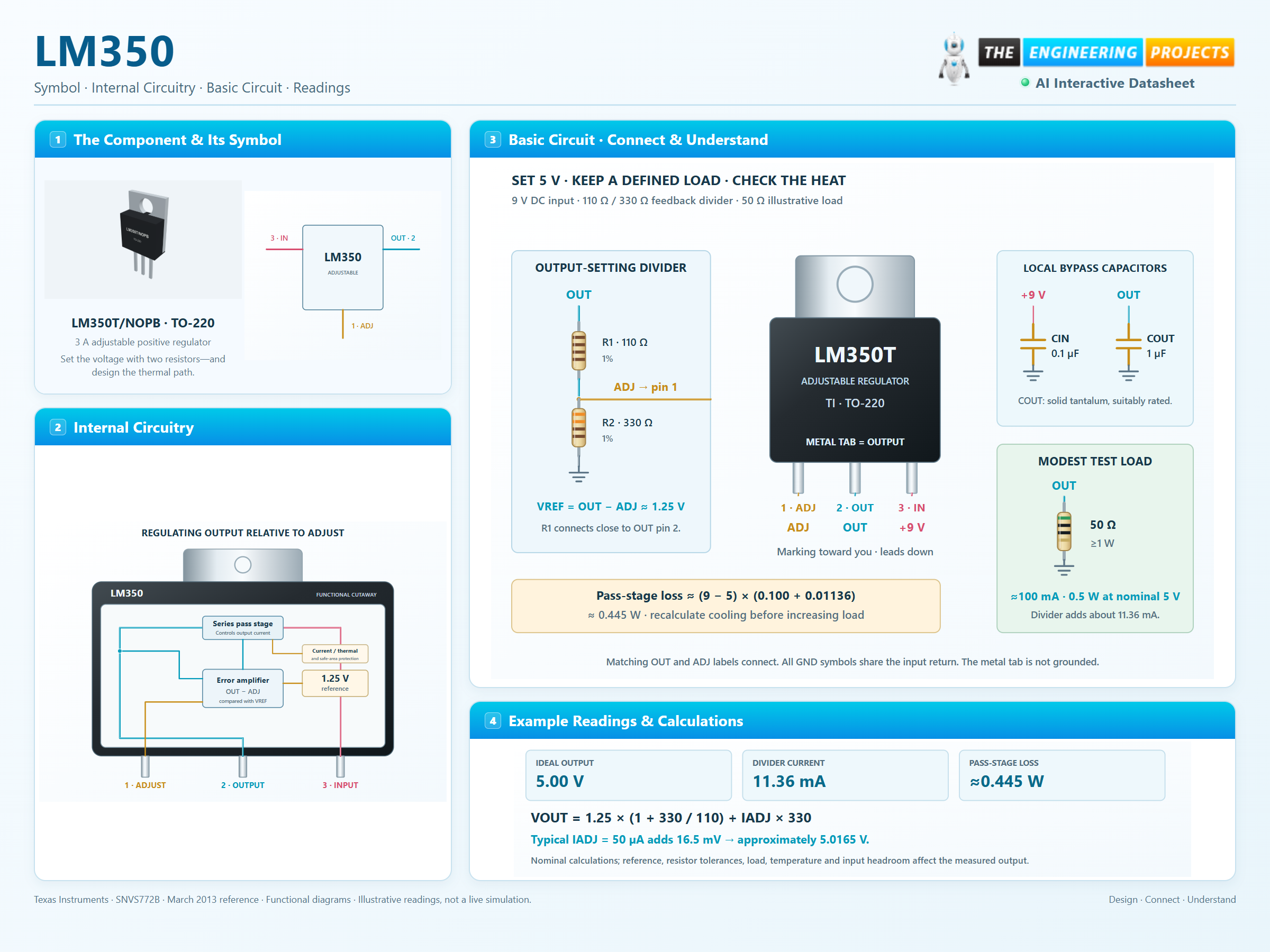
3 stages · Explore one step at a time
The regulator controls OUTPUT relative to ADJUST, not directly relative to ground.
Connect 110 Ω from OUT to ADJ and 330 Ω from ADJ to the return. The nominal ratio is three to one.
The divider draws about 11.36 mA. Add the load current before calculating pass-stage dissipation and selecting cooling.
A physical TO-220 regulator with a feedback divider and a modest load.
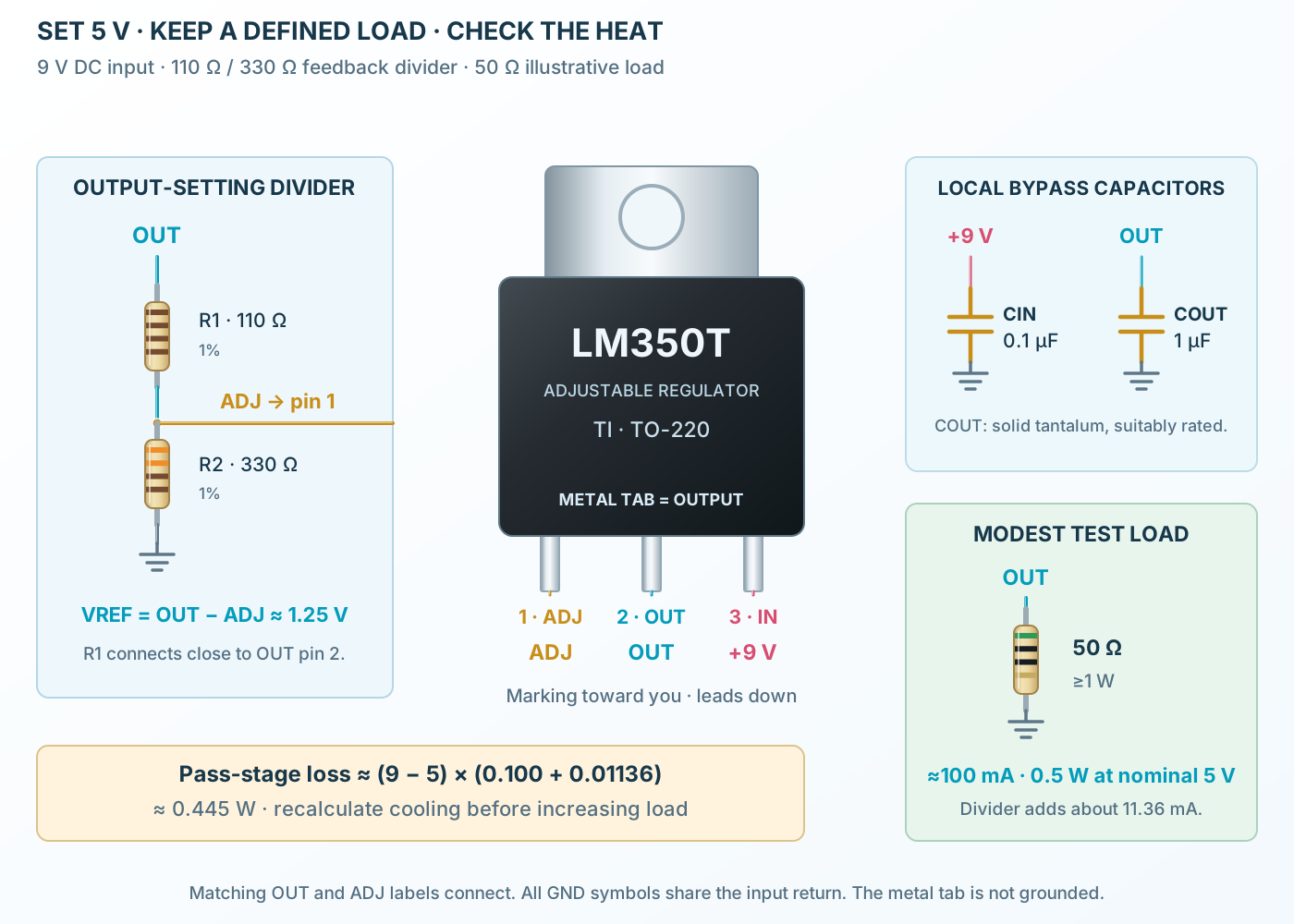
Follow the component values and pin connections
With the marking toward you, the left, middle and right leads are ADJ, OUT and IN.
110 Ω from OUT to ADJ and 330 Ω from ADJ to ground set nominal 5 V; the 50 Ω load draws about 100 mA.
The nominal pass-stage loss is about 0.45 W here. Recalculate before increasing voltage or current.
A compact floating reference and pass-control loop inside the package.
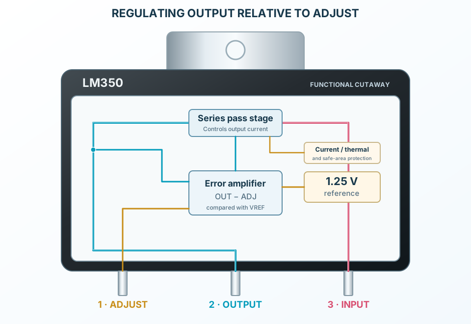
Select a stage to see its role and connections
The reference establishes approximately 1.25 V between these terminals.
An error amplifier adjusts current from INPUT to OUTPUT.
Current limiting, thermal protection and safe-area control constrain the pass stage.
Signal names, electrical functions and connection guidance
Scroll within the table to see all columns and rows.
| Pin | Signal | Type | Function & connection |
|---|---|---|---|
| ADJUST | Floating reference terminal | The loop regulates OUTPUT approximately 1.25 V above ADJUST.Connection guidanceConnect the junction of R1 from OUTPUT and R2 to the return. This is not ground; adjustment-pin current contributes IADJ × R2 to output voltage. | |
| OUTPUT | Regulated output and tab | Supplies the external load and feedback divider. The metal tab is electrically connected to OUTPUT.Connection guidanceConnect R1 close to this lead and return R2 near the load return. A grounded heatsink needs appropriate electrical insulation from the live output tab. | |
| INPUT | Unregulated input | Powers the series pass stage.Connection guidanceUse +9 V in the example, with a local 0.1 µF bypass to the common return. Keep adequate headroom. The 35 V stress limit is input-to-output differential. |
No pins match these filters. Try another signal name or reset the filters.
Standard LM350 · not LM350A
Scroll within the table to see all columns and rows.
| Parameter | Value | Conditions / notes |
|---|---|---|
| Nominal adjustable output | 1.2–33 V | With sufficient input headroom and load |
| Operating junction temperature | 0–125°C | This is junction, not ambient temperature |
| Reference voltage | 1.20 / 1.25 / 1.30 V | Minimum / typical / maximum; stated electrical conditions |
| Adjustment-pin current | 50 µA typical; 100 µA maximum | Flows out of ADJUST |
| Adjustment current change | 0.2 µA typical; 5 µA maximum | 10 mA–3 A; 3–35 V differential |
| Input-to-output absolute maximum | 35 V | Differential stress limit, not an unconditional input rating |
No specifications match. Try a parameter name or a unit.
Electrical reference conditions include 3–35 V differential and specified loads; TO-220 dissipation is limited by the source footnote and thermal design.
Manufacturer test conditions retained
Scroll within the table to see all columns and rows.
| Parameter | Value | Conditions / notes |
|---|---|---|
| Line regulation at 25°C | 0.005%/V typical; 0.03%/V maximum | 3–35 V input-output differential |
| Line regulation over junction range | 0.02%/V typical; 0.07%/V maximum | Standard LM350 limits |
| Load regulation at 25°C | 0.1% typical; 0.5% maximum | 10 mA–3 A |
| Load regulation over junction range | 0.3% typical; 1.5% maximum | Pulse-tested at constant junction temperature |
| Thermal regulation | 0.002%/W typical; 0.03%/W maximum | 20 ms pulse; 25°C |
| Ripple rejection without CADJ | 65 dB typical | 10 V output, 120 Hz, 25°C |
| Ripple rejection with 10 µF CADJ | 66 dB minimum; 86 dB typical | 10 V output, 120 Hz; applicable full-range limit |
No specifications match. Try a parameter name or a unit.
Typical figures do not replace guaranteed limits. The LM350A column has tighter accuracy and is not used here.
Cooling and differential voltage matter
Scroll within the table to see all columns and rows.
| Parameter | Value | Conditions / notes |
|---|---|---|
| Minimum load requirement | 3.5 mA typical; 10 mA maximum | At 35 V differential |
| Current-limit capability at ≤10 V differential | 3 A minimum; 4.5 A typical | Within specified power and junction limits |
| Current limit at 30 V differential | 0.25 A minimum; 1 A typical | Safe-area protection reduces available current |
| Example divider current | 1.25 V / 110 Ω ≈11.36 mA | Nominal OUT-to-ADJ branch |
| Divider worst-case minimum | 1.20 V / 111.1 Ω ≈10.80 mA | 110 Ω resistor at +1%; above 10 mA |
| Too little output load | Output can rise above the set value | Do not rely only on typical minimum current |
No specifications match. Try a parameter name or a unit.
The 3 A label is not a guarantee at every voltage differential or without a heatsink.
LM350T · TO-220 NDE
Scroll within the table to see all columns and rows.
| Parameter | Value | Conditions / notes |
|---|---|---|
| Junction-to-case resistance | 3°C/W typical; 4°C/W maximum | Manufacturer NDE package reference |
| Junction-to-ambient reference | 50°C/W | No heatsink; actual mounting and airflow matter |
| Pass-stage estimate | PD ≈ (VIN − VOUT) × IOUT | Include divider current in output current |
| Example at 100 mA load | (9 − 5) × (0.100 + 0.01136) ≈0.445 W | Nominal estimate; adjustment current term is small |
| At 3 A and 4 V drop | Approximately 12 W | Requires a carefully designed thermal path |
| Built-in protections | Current, thermal and safe-area limiting | Protection is not normal operating regulation |
| Metal tab | Electrically OUTPUT | Insulate from grounded metal when required |
No specifications match. Try a parameter name or a unit.
Calculate junction temperature with case/interface/heatsink resistances and the actual ambient.
Source application guidance
Scroll within the table to see all columns and rows.
| Parameter | Value | Conditions / notes |
|---|---|---|
| Input bypass | 0.1 µF ceramic or 1 µF solid tantalum | Close to the regulator and return |
| Output capacitor | 1 µF solid tantalum or 25 µF aluminum | Improves transient response; not an arbitrary ceramic substitution |
| No output capacitor | The regulator can be stable without one | Certain small capacitances can cause ringing |
| Adjustment bypass | 10 µF improves ripple rejection | Optional; evaluate discharge protection |
| Output discharge protection | Review for large stored output charge | Source states ≤25 µF output capacitors need no diode in its discussed case |
| Adjustment discharge protection | Depends on CADJ and output voltage | Follow source Figure 17 for larger capacitance / voltage cases |
No specifications match. Try a parameter name or a unit.
The example uses 0.1 µF input and 1 µF tantalum output, with no ADJ bypass. Review protection if external supplies or stored charge can drive the output.
110 Ω / 330 Ω divider · 50 Ω load
Scroll within the table to see all columns and rows.
| Parameter | Value | Conditions / notes |
|---|---|---|
| R1; OUT2 to ADJ1 | 110 Ω, 1% | Dissipates about 14.2 mW at nominal reference |
| R2; ADJ1 to GND | 330 Ω, 1% | Nominal ratio R2/R1 = 3 |
| Ideal output | 1.25 × (1 + 330/110) = 5.00 V | Before IADJ and tolerances |
| Including typical adjustment current | 5.0165 V | Adds 50 µA × 330 Ω |
| Load resistor | 50 Ω, at least 1 W | Nominal 100 mA and 0.5 W |
| Nominal total output current | 111.36 mA | Load plus divider; small IADJ contribution omitted |
| Return connections | Input return, R2, load and capacitor returns | Same GND net; ADJ is not GND |
No specifications match. Try a parameter name or a unit.
Use adequate resistor/capacitor ratings and verify the actual loaded voltage.
LM350T/NOPB · TO-220
Scroll within the table to see all columns and rows.
| Parameter | Value | Conditions / notes |
|---|---|---|
| Front-view leads | 1 ADJUST; 2 OUTPUT; 3 INPUT | Marking toward you, leads down |
| Lead pitch | 2.54 mm | Vertical three-lead footprint |
| Tab connection | OUTPUT | Not ground |
| Selected package | TO-220 NDE | Original TEP geometry and starting footprint |
| Other source package | TO-3 is described in the manufacturer sheet | Different physical terminal arrangement; not interchangeable footprint |
| Storage temperature | −65 to +150°C | Unpowered storage |
No specifications match. Try a parameter name or a unit.
This page publishes the verified TO-220 variant; no unsupported SMD substitute is implied.
No matching rowsTry a pin name, parameter, unit or test condition, or reset the filters.
Set a positive rail with a divider and suitable thermal design.
Manufacturer application guideUse the manufacturer’s reference-resistor configuration to establish a current, within voltage and power limits.
Manufacturer application guideExplore reference tolerances, minimum load, headroom and heat with a modest DC supply.
Manufacturer application guideFind LM350 in the Components Library to place its schematic symbol and connect its pins.
Reference page · circuit simulation model not yet availableOpen ProTech