Real View
Give a small analog signal a useful gain.
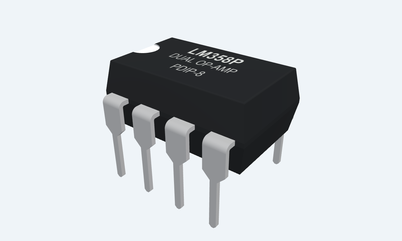
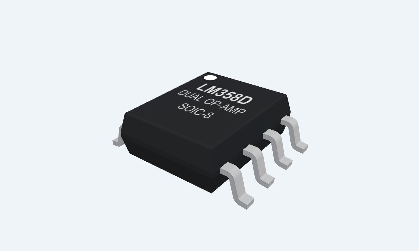
LM358 contains two independent operational amplifiers in one eight-pin package. Both channels share the supply pins. Negative feedback sets a useful closed-loop gain. The inputs can operate near ground, but the output does not reach the positive supply rail. This page covers the classic LM358P in PDIP-8 and LM358D in SOIC-8.
Select a pin to explore its connection
Click a lead or use the arrow keys. Top view
Amplifier A output.
Feed back to IN1− through Rf; connect the measured output here.
Allow output headroom; do not treat it as a rail-to-rail output.
Amplifier A feedback input.
Connect the junction of Rf and Rg here.
Negative feedback controls the gain while the amplifier is operating linearly.
Amplifier A signal input.
Connect the input signal and its common ground.
Keep within the recommended common-mode range.
Lowest supply potential for both channels.
Connect to ground in the illustrated single-supply circuit.
Amplifier B signal input.
In this example, connect to VIN so the spare channel acts as a buffer.
Amplifier B feedback input.
Connect directly to OUT2 for a unity-gain follower.
Amplifier B output.
Connect to IN2−; leave the buffered output otherwise unloaded.
Do not tie the two outputs together.
Highest supply potential for both channels.
Connect to +5 V and place a 100 nF bypass capacitor to pin 4 nearby.
One package, two signal paths. Set their gains with external feedback.
LM358P · PDIP-8
| Property | Details |
|---|---|
| Manufacturer | Texas Instruments |
| Part number | LM358P |
| Package | PDIP-8 |
| Connections | 8 pins |
| Mounting | Through-hole |
| Lead pitch | 2.54 mm |
| Package code | P |
| Thermal reference | Board-dependent; see TI thermal table |
Classic LM358P / LM358D
Scroll sideways to see all columns.
| Parameter | Value | Conditions / notes |
|---|---|---|
| Supply difference | 3–30 V | Recommended operating range |
| Ambient temperature | 0–70°C | LM358 grade |
| Input common-mode range | V− to V+ − 2 V | Recommended operating conditions |
| Supply absolute maximum | 32 V | Stress rating, not an operating target |
No specifications match. Try a parameter name or a unit.
TI SLOS068AB, sections 5.1 and 5.3.
Typical values are not production guarantees
Scroll sideways to see all columns.
| Parameter | Value | Conditions / notes |
|---|---|---|
| Gain-bandwidth product | 0.7 MHz typical | Classic LM358 |
| Slew rate | 0.3 V/µs typical | Unity gain |
| Input offset voltage | 3 mV typical; 7 mV maximum | 25°C; see manufacturer test conditions |
| Input bias current | 20 nA typical magnitude | 25°C |
| Supply current | 350 µA typical per channel | 5 V; unloaded; 0–70°C test row |
| High-side output headroom | 1.5 V typical | 5 V supply, RL ≥ 2 kΩ |
| Near-ground output | 5 mV typical; 20 mV maximum | 5 V; RL ≤ 10 kΩ; 0–70°C |
No specifications match. Try a parameter name or a unit.
TI SLOS068AB, section 5.7. Conditions differ between rows; consult the PDF before selecting a part.
Non-inverting DC example
Scroll sideways to see all columns.
| Parameter | Value | Conditions / notes |
|---|---|---|
| Closed-loop gain | 1 + Rf / Rg | Within the linear operating region |
| Example resistors | Rf = 20 kΩ; Rg = 10 kΩ | Gain = 3 |
| Example input / ideal output | 0.50 V / 1.50 V | Calculated, not a measured result |
| Explorer clipping ceiling | 3.50 V | Illustrative 5 V − 1.5 V headroom |
| Explorer input limit | 3.00 V | 5 V − 2 V recommended common-mode headroom |
No specifications match. Try a parameter name or a unit.
The explorer uses a fixed DC headroom approximation. It omits offset, bias, noise, frequency, temperature and load-dependent effects.
LM358P · PDIP-8
Scroll sideways to see all columns.
| Parameter | Value | Conditions / notes |
|---|---|---|
| Mounting | Through-hole | Selected physical package |
| Lead pitch | 2.54 mm | Check land pattern dimensions before PCB manufacture |
| Pin mapping | 8 numbered pins | Same functions in PDIP-8 and SOIC-8 |
| Orientation | Top view | Use the notch / pin-1 marker |
No specifications match. Try a parameter name or a unit.
The package selector updates all four views together.
Select a pin for its function, connection guidance and electrical notes.
Follow the labeled connections and functional stages
3 stages · Explore one step at a time
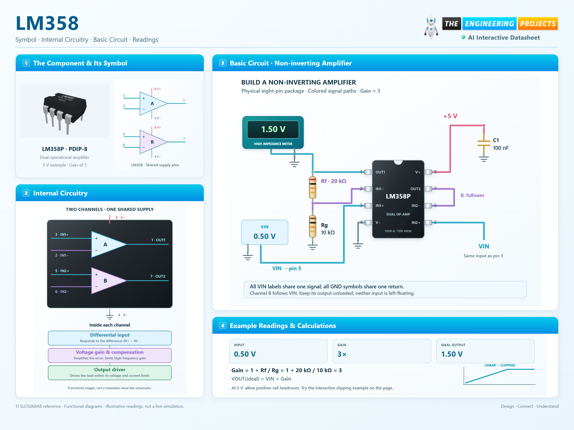
The amplifier responds to the difference between its + and − inputs. A small difference can produce a large output change without feedback.
Rf returns part of OUT1 to IN1−. Rg connects that node to ground. In the linear region, the circuit settles with approximately equal input voltages.
With Rf = 20 kΩ and Rg = 10 kΩ, the ideal gain is 3. An input of 0.50 V requests 1.50 V at the output. Raising the input eventually runs into the output headroom.
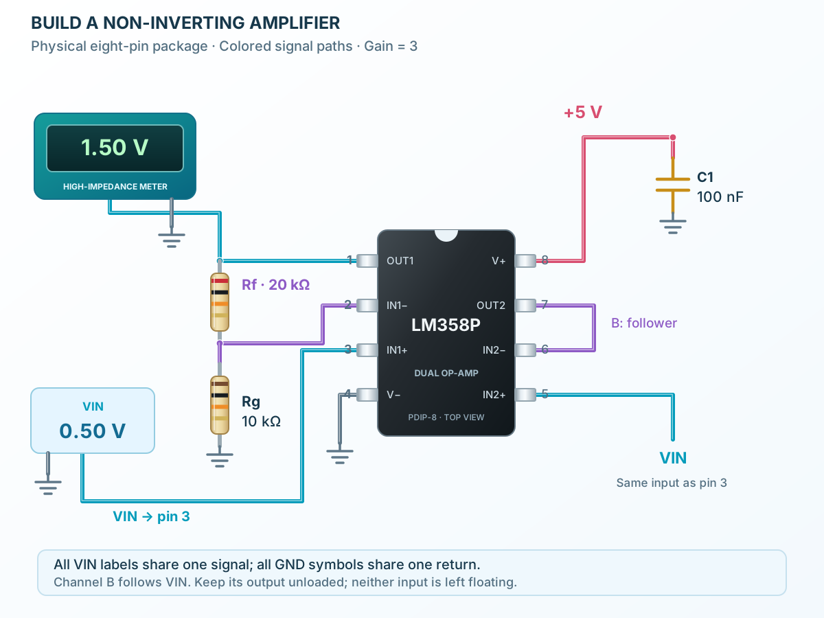
A physical PDIP-8 package, two gain-setting resistors and clear signal wiring.
Follow the component values and pin connections
Connect V+ (8) to +5 V and V− (4) to ground. Place 100 nF between the rails near the IC.
Connect VIN to pin 3. Put 20 kΩ between pins 1 and 2, and 10 kΩ from pin 2 to ground. Measure at pin 1.
Connect pin 5 to the same VIN and join pins 6 and 7. Channel B follows VIN with no extra load; its inputs are not left floating.
Change the input and feedback. See the gain and output respond.
Enable JavaScript to explore the amplifier.
Gain = 1 + Rf / Rg · VOUT(ideal) = VIN × Gain
Illustrative DC model at 5 V with a light load: 3.50 V upper output and 0.02 V lower output. Real headroom depends on load, temperature and part variation. Offset, bandwidth, slew rate and noise are omitted; use the ProTech example for a running simulation.
Two amplifiers, a shared supply and a controlled feedback path.
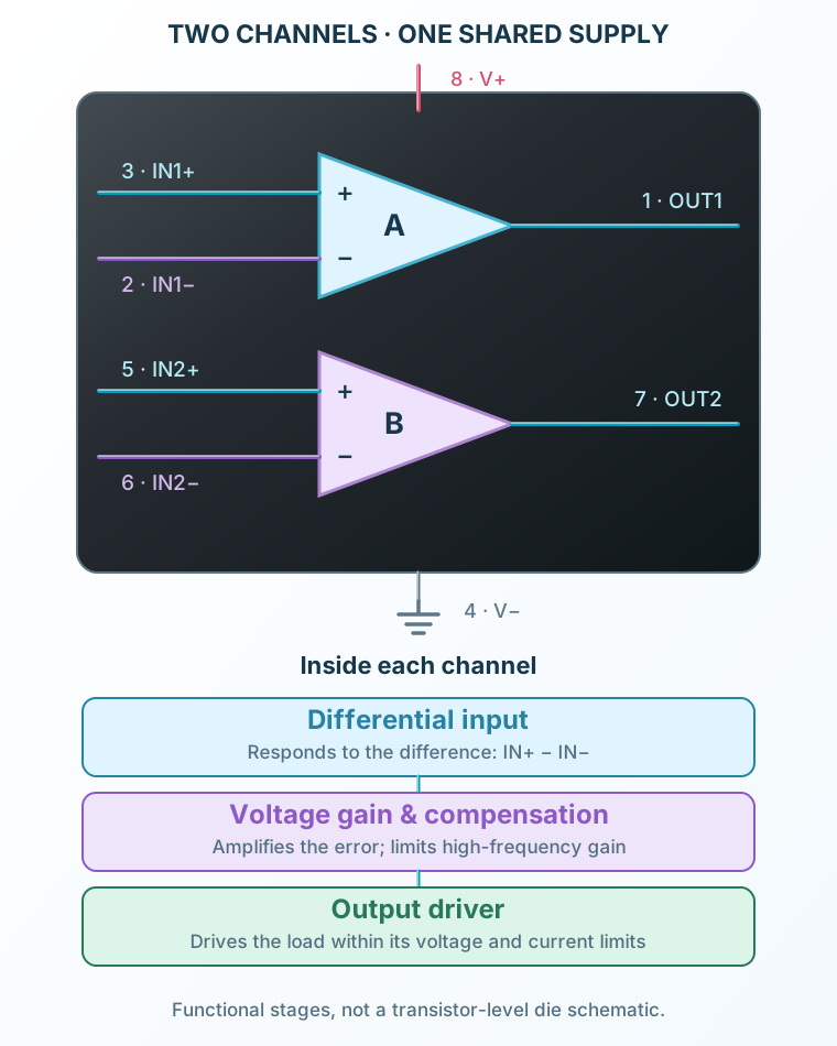
Select a stage to see its role and connections
Channel A uses pins 1, 2 and 3. Channel B uses pins 5, 6 and 7. Their outputs are independent.
Pins 8 and 4 power both channels. Decouple the supply close to the package.
External feedback controls the relationship between input and output. Compensation helps stability, while output swing and speed remain finite.
Signal names, electrical functions and connection guidance
Scroll within the table to see all columns and rows.
| Pin | Signal | Type | Function & connection |
|---|---|---|---|
| OUT1 | Output | Amplifier A output.Connection guidanceFeed back to IN1− through Rf; connect the measured output here. Allow output headroom; do not treat it as a rail-to-rail output. | |
| IN1− | Inverting input | Amplifier A feedback input.Connection guidanceConnect the junction of Rf and Rg here. Negative feedback controls the gain while the amplifier is operating linearly. | |
| IN1+ | Non-inverting input | Amplifier A signal input.Connection guidanceConnect the input signal and its common ground. Keep within the recommended common-mode range. | |
| V− | Supply return | Lowest supply potential for both channels.Connection guidanceConnect to ground in the illustrated single-supply circuit. | |
| IN2+ | Non-inverting input | Amplifier B signal input.Connection guidanceIn this example, connect to VIN so the spare channel acts as a buffer. | |
| IN2− | Inverting input | Amplifier B feedback input.Connection guidanceConnect directly to OUT2 for a unity-gain follower. | |
| OUT2 | Output | Amplifier B output.Connection guidanceConnect to IN2−; leave the buffered output otherwise unloaded. Do not tie the two outputs together. | |
| V+ | Positive supply | Highest supply potential for both channels.Connection guidanceConnect to +5 V and place a 100 nF bypass capacitor to pin 4 nearby. |
No pins match these filters. Try another signal name or reset the filters.
Classic LM358P / LM358D
Scroll within the table to see all columns and rows.
| Parameter | Value | Conditions / notes |
|---|---|---|
| Supply difference | 3–30 V | Recommended operating range |
| Ambient temperature | 0–70°C | LM358 grade |
| Input common-mode range | V− to V+ − 2 V | Recommended operating conditions |
| Supply absolute maximum | 32 V | Stress rating, not an operating target |
No specifications match. Try a parameter name or a unit.
TI SLOS068AB, sections 5.1 and 5.3.
Typical values are not production guarantees
Scroll within the table to see all columns and rows.
| Parameter | Value | Conditions / notes |
|---|---|---|
| Gain-bandwidth product | 0.7 MHz typical | Classic LM358 |
| Slew rate | 0.3 V/µs typical | Unity gain |
| Input offset voltage | 3 mV typical; 7 mV maximum | 25°C; see manufacturer test conditions |
| Input bias current | 20 nA typical magnitude | 25°C |
| Supply current | 350 µA typical per channel | 5 V; unloaded; 0–70°C test row |
| High-side output headroom | 1.5 V typical | 5 V supply, RL ≥ 2 kΩ |
| Near-ground output | 5 mV typical; 20 mV maximum | 5 V; RL ≤ 10 kΩ; 0–70°C |
No specifications match. Try a parameter name or a unit.
TI SLOS068AB, section 5.7. Conditions differ between rows; consult the PDF before selecting a part.
Non-inverting DC example
Scroll within the table to see all columns and rows.
| Parameter | Value | Conditions / notes |
|---|---|---|
| Closed-loop gain | 1 + Rf / Rg | Within the linear operating region |
| Example resistors | Rf = 20 kΩ; Rg = 10 kΩ | Gain = 3 |
| Example input / ideal output | 0.50 V / 1.50 V | Calculated, not a measured result |
| Explorer clipping ceiling | 3.50 V | Illustrative 5 V − 1.5 V headroom |
| Explorer input limit | 3.00 V | 5 V − 2 V recommended common-mode headroom |
No specifications match. Try a parameter name or a unit.
The explorer uses a fixed DC headroom approximation. It omits offset, bias, noise, frequency, temperature and load-dependent effects.
LM358P · PDIP-8
Scroll within the table to see all columns and rows.
| Parameter | Value | Conditions / notes |
|---|---|---|
| Mounting | Through-hole | Selected physical package |
| Lead pitch | 2.54 mm | Check land pattern dimensions before PCB manufacture |
| Pin mapping | 8 numbered pins | Same functions in PDIP-8 and SOIC-8 |
| Orientation | Top view | Use the notch / pin-1 marker |
No specifications match. Try a parameter name or a unit.
The package selector updates all four views together.
No matching rowsTry a pin name, parameter, unit or test condition, or reset the filters.
Apply a small analog sensor output to a non-inverting stage. Choose gain for the signal range, ADC reference and available output swing.
Manufacturer application guideUse a follower when the voltage should remain similar but the following circuit needs a lower source impedance. Check input and output limits.
Manufacturer application guideCombine resistance, capacitance and feedback to filter a slow signal. Evaluate bandwidth, loading and settling in the complete circuit.
Manufacturer application guideFind LM358 in the Components Library to place its schematic symbol and connect its pins.
Simulation model available · Open the adjustable amplifierOpen ProTech