LM386Low-voltage audio power amplifier
Take a small audio signal all the way to a speaker.
LM386 is an 8-pin mono audio power amplifier that can drive a small speaker from a low-voltage supply. Unlike a general-purpose op-amp, its internal feedback gives a useful audio gain with very few external parts. With pins 1 and 8 open, the voltage gain is approximately 20. A capacitor across those pins can raise AC gain to 200, while the output capacitor keeps the amplifier’s DC bias out of the speaker. This page uses LM386N-1 in PDIP-8 and LM386M-1 in SOIC-8. Both use a 4–12 V supply range; the higher-voltage LM386N-4 limits must not be applied to these parts.
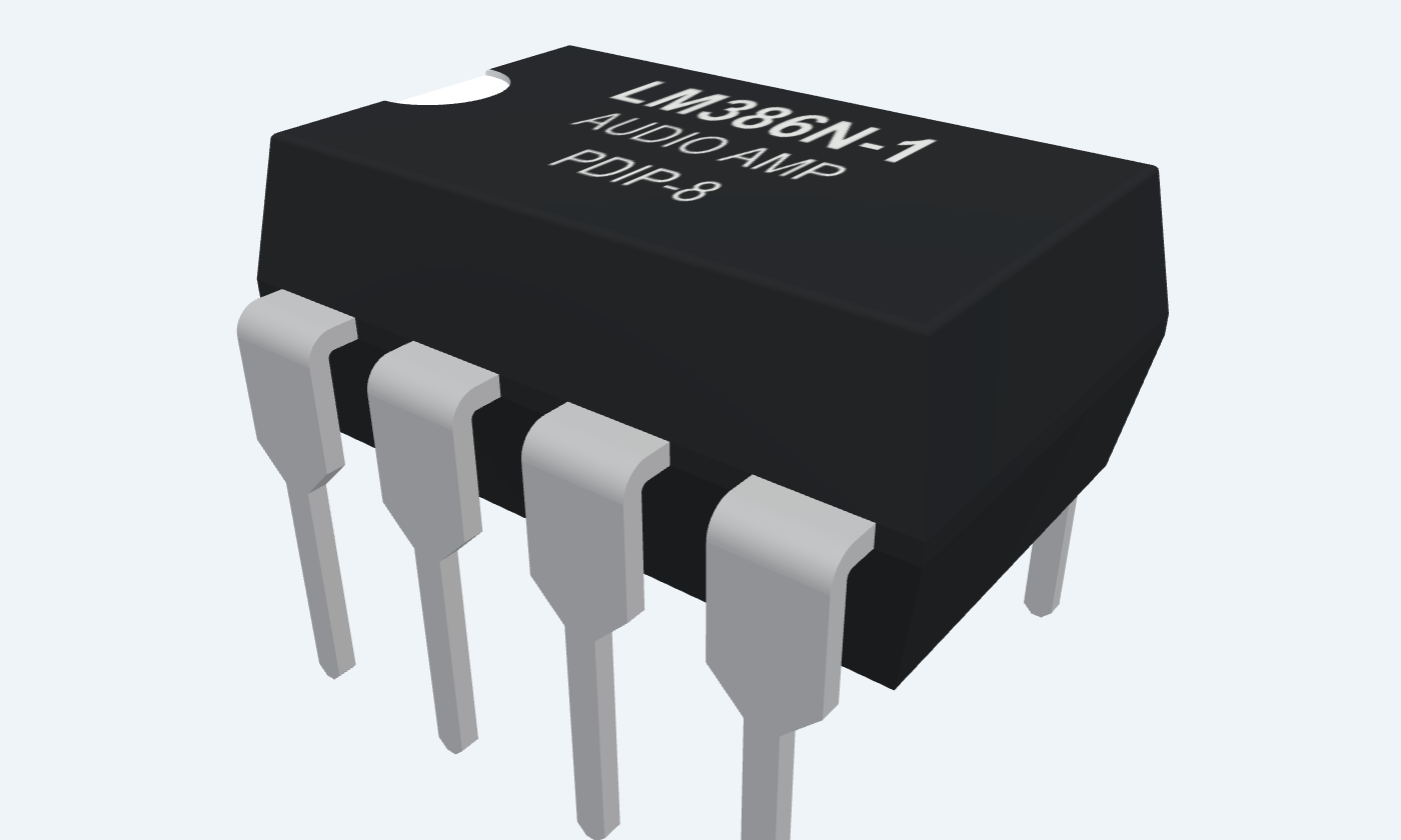
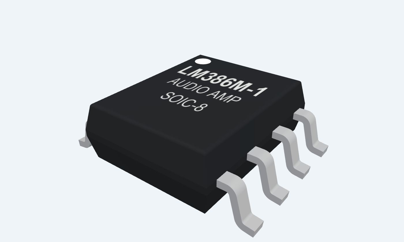

8Physical pins
LM386N-1PDIP-8
Manufacturer-referencedTexas Instruments
Pin diagram
Select a pin to explore its connection
Highlight
LM386N-1PDIP-8Top view
LM386M-1SOIC-8Top view
Click a lead or use the arrow keys. Top view
PIN 1 · Gain & bypass
Gain adjustmentGAIN
Function
One end of the internal gain-setting network.
How to connect
Leave open for gain 20; a 10 µF capacitor from pin 1 to pin 8 raises AC gain to about 200.
Electrical note
Positive capacitor terminal at pin 1.
PIN 2 · Audio inputs
Inverting input−INPUT
Function
Ground-referenced inverting signal input.
How to connect
Connect to signal ground in the non-inverting speaker example.
PIN 3 · Audio inputs
Non-inverting input+INPUT
Function
Ground-referenced audio input.
How to connect
Feed a small AC signal through the input coupling capacitor.
Electrical note
Keep input excursions inside ±0.4 V.
PIN 4 · Ground
GroundGND
Function
Input, bypass and power return reference.
How to connect
Connect to supply negative; keep input returns away from speaker-current paths.
PIN 5 · Speaker drive
Audio outputVOUT
Function
Output sits near half the supply at rest; the audio waveform rides on this DC level.
How to connect
Use a series output capacitor before the speaker. Connect a 10 Ω + 47 nF series network from output to GND.
Electrical note
Do not connect an ordinary low-impedance speaker directly between this pin and GND.
PIN 6 · Supply
Positive supplyVS
Function
Supply for the amplifier output and bias circuits.
How to connect
Use +6 V in this example with local 100 nF and 100 µF bypass capacitors.
Electrical note
4–12 V for the selected -1 variants.
PIN 7 · Gain & bypass
Bias bypassBYPASS
Function
Decoupling access to the internal bias network.
How to connect
An optional 10 µF capacitor to GND improves supply rejection.
Electrical note
Capacitor positive at pin 7.
PIN 8 · Gain & bypass
Gain adjustmentGAIN
Function
The second end of the gain-setting network.
How to connect
Leave open with pin 1 for gain 20.
Electrical note
A capacitor or series RC between 1 and 8 changes gain; it is not a supply pin.
Key specifications
A ground-referenced input, internally set gain and a biased power output make a compact mono amplifier. The speaker needs AC coupling.
Selected -1 supply range4–12 V
Voltage gain20–200 Set with pins 1 and 8
Ambient range0–70 °C
Typical power at 6 V325 mW · 8 Ω · 10% THD
Package details
LM386N-1 · PDIP-8
| Property | Details |
|---|---|
| Manufacturer | Texas Instruments |
| Part number | LM386N-1 |
| Package | PDIP-8 |
| Connections | 8 pins |
| Mounting | Through-hole |
| Lead pitch | 2.54 mm |
| Package code | dip |
| Thermal reference | Board and package dependent; see manufacturer data |
Operating conditions
LM386N-1 / LM386M-1
Manufacturer specifications 5 parameters
Scroll sideways to see all columns.
| Parameter | Value | Conditions / notes |
|---|---|---|
| Supply voltage | 4–12 V | Selected -1 variants |
| Ambient temperature | 0 to 70°C | Operating range |
| Speaker impedance | 4 Ω minimum | Use the power curves for the selected supply and load |
| Input range | −0.4 to +0.4 V | Relative to GND |
| Quiescent current | 4 mA typical; 8 mA maximum | VS = 6 V; VIN = 0 |
No specifications match. Try a parameter name or a unit.
The LM386N-4 is a different option with a 5–18 V operating range.
Audio performance
Conditions matter
Manufacturer specifications 8 parameters
Scroll sideways to see all columns.
| Parameter | Value | Conditions / notes |
|---|---|---|
| Default voltage gain | 20 V/V · 26 dB | 6 V; 1 kHz; pins 1 and 8 open |
| High-gain configuration | 200 V/V · 46 dB | 10 µF between pins 1 and 8 |
| Bandwidth | 300 kHz typical | 6 V; gain 20 |
| Output power | 250 mW minimum; 325 mW typical | 6 V; 8 Ω; 10% THD; selected -1 variants |
| Distortion | 0.2% typical | 6 V; 8 Ω; 125 mW; 1 kHz; gain 20 |
| Input resistance | 50 kΩ typical | Small-signal input |
| Input bias current | 250 nA typical | 6 V; inputs open |
| Supply rejection | 50 dB typical | 6 V; 1 kHz; 10 µF bypass; gain pins open |
No specifications match. Try a parameter name or a unit.
The 10% THD power rating is not a low-distortion listening target.
Speaker circuit
6 V · gain 20 · 8 Ω
Manufacturer specifications 8 parameters
Scroll sideways to see all columns.
| Parameter | Value | Conditions / notes |
|---|---|---|
| Input coupling C1 | 100 nF | Audio source to input3; 100 kΩ input return |
| Input return R1 | 100 kΩ | Input3 to GND; internal input resistance also loads it |
| Output coupling C2 | 250 µF | Positive side at output5; speaker side near 0 V DC |
| Output stability network | 10 Ω in series with 47 nF | Output5 to GND; place close to the IC |
| Supply bypass | 100 nF + 100 µF | VS6 to GND4 |
| Bias bypass | 10 µF optional | Pin7 to GND; positive at pin7 |
| Gain pins | 1 and 8 open | Gain approximately 20 |
| Speaker high-pass corner | 79.6 Hz nominal | 1 / (2π × 8 Ω × 250 µF) |
No specifications match. Try a parameter name or a unit.
Speaker impedance varies with frequency; the calculator treats it as an 8 Ω resistor.
Gain configurations
Pins 1 and 8
Manufacturer specifications 5 parameters
Scroll sideways to see all columns.
| Parameter | Value | Conditions / notes |
|---|---|---|
| Open pins | Gain ≈ 20 | Fewest external parts |
| 10 µF capacitor | Gain ≈ 200 | Positive at pin1; negative at pin8 |
| 10 µF + 1.2 kΩ in series | Gain ≈ 50 | Manufacturer example |
| More gain | More sensitivity and amplified noise | Reduce source level to avoid clipping |
| Output at rest | Approximately VS / 2 | Not a ground-referenced DC output |
No specifications match. Try a parameter name or a unit.
These are AC gain configurations; they do not turn the device into a rail-to-rail precision op-amp.
Package and stress limits
LM386N-1 · PDIP-8
Manufacturer specifications 5 parameters
Scroll sideways to see all columns.
| Parameter | Value | Conditions / notes |
|---|---|---|
| Lead pitch | 2.54 mm | Through-hole; top view |
| Supply absolute maximum | 15 V | Selected -1 variants; stress rating only |
| Input absolute maximum | ±0.4 V | Respect signal amplitude and transients |
| Storage temperature | −65 to +150°C | Unpowered |
| Thermal design | Package and PCB dependent | Check dissipation and thermal resistance for the actual layout |
No specifications match. Try a parameter name or a unit.
Absolute maximum limits are not recommended operating targets.
Connections by function
Select a pin for its function, connection guidance and electrical notes.
Gain & bypass3 pins
Audio inputs2 pins
Ground1 pin
Speaker drive1 pin
Supply1 pin
Gain & bypass3 pins
Audio inputs2 pins
Ground1 pin
Speaker drive1 pin
Supply1 pin
LM386 at a glance
Follow the labeled connections and functional stages
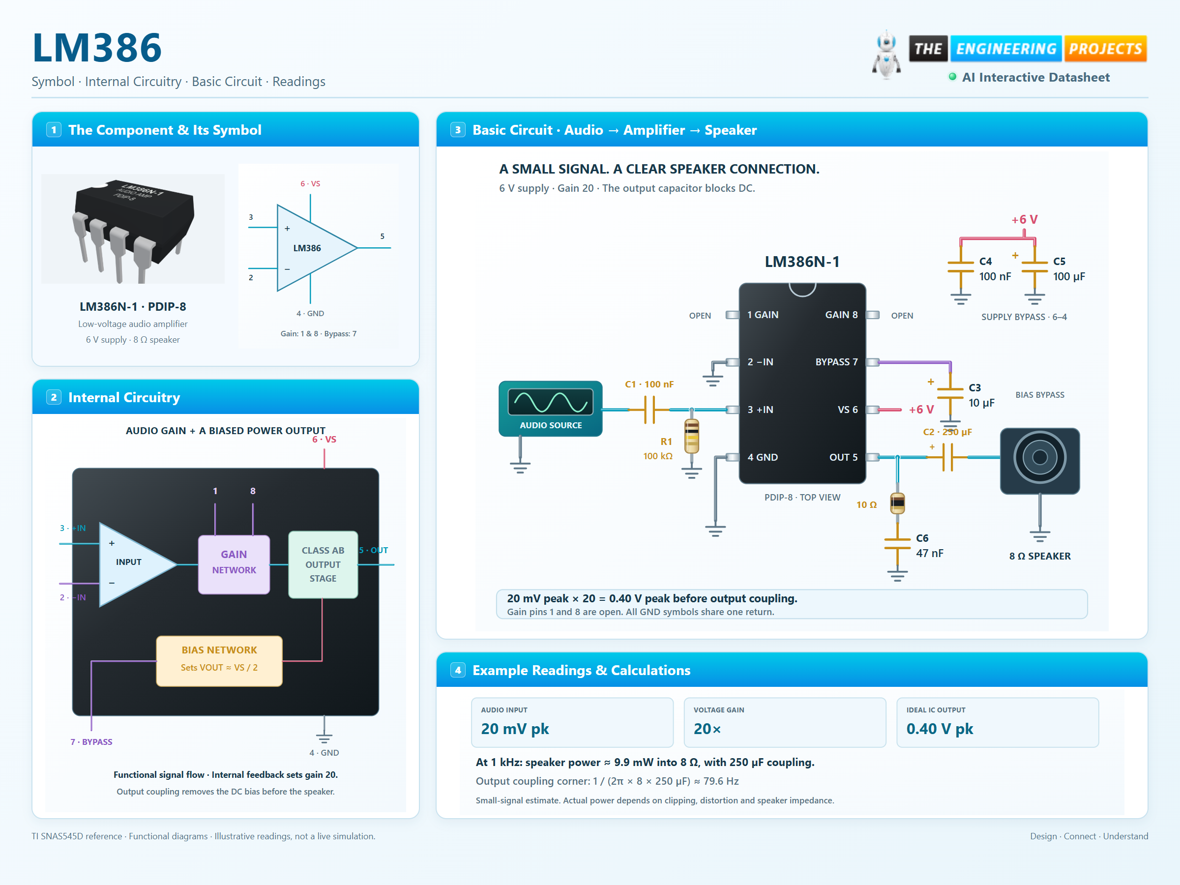
How it works
3 stages · Explore one step at a time
Feed a ground-referenced signal
The input stage accepts a small audio waveform around ground. Coupling and volume control keep the applied level appropriate.
Set the AC gain
Internal feedback sets gain 20. Bypassing the gain network with a capacitor between pins 1 and 8 increases gain; higher gain also amplifies noise.
Remove the DC before the speaker
The output rests near half the supply. A large series capacitor blocks this DC level while passing the changing audio signal.
Step 1 of 3
From millivolts to speaker power
Change gain and frequency to explore amplification and output coupling.
Requested IC peak—
Speaker power—
Coupling corner—
Enable JavaScript to explore audio gain.
Teaching model: ideal gain, an RC output coupling network and an illustrative ±2 V peak output limit. The limit is not a guaranteed LM386 clipping specification. Speaker impedance, bandwidth, noise, distortion and thermal effects are not simulated.
LM386 in a circuit
A real IC, AC coupling and a clearly connected speaker.
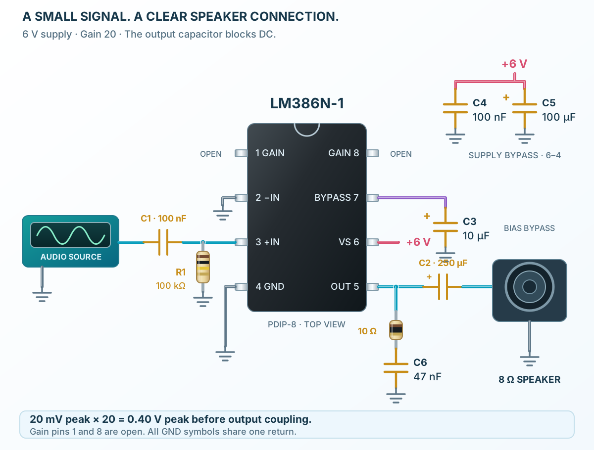
Connect it, step by step
Follow the component values and pin connections
Keep the input quiet
Use short signal wiring and a common ground. The input capacitor blocks source DC.
Decouple the supply
Put the small bypass capacitor close to pins 6 and 4, and add local bulk capacitance.
Connect the speaker through C2
The positive side of the output capacitor faces pin 5, which sits near half the supply.
Inside LM386
Audio input, gain control, bias and power output.
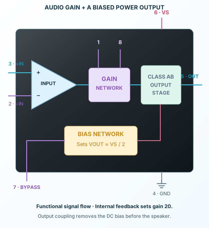
Explore the circuit
Select a stage to see its role and connections
Differential input
Pins 2 and 3 accept a small differential audio signal.
Internal feedback
The gain network sets gain 20 without an external feedback resistor.
Biased output stage
A push-pull power stage supplies the load. Its half-supply DC level is removed by the speaker coupling capacitor.
Selected packagePDIP-8LM386N-1
Physical connections8 pinsPackage-specific numbering
Reference collection6 tables31 parameters & pin functions
Pin reference
Signal names, electrical functions and connection guidance
Physical pin numbers8 pins
Scroll within the table to see all columns and rows.
| Pin | Signal | Type | Function & connection |
|---|---|---|---|
| GAIN | Gain adjustment | One end of the internal gain-setting network.Connection guidanceLeave open for gain 20; a 10 µF capacitor from pin 1 to pin 8 raises AC gain to about 200. Positive capacitor terminal at pin 1. | |
| −INPUT | Inverting input | Ground-referenced inverting signal input.Connection guidanceConnect to signal ground in the non-inverting speaker example. | |
| +INPUT | Non-inverting input | Ground-referenced audio input.Connection guidanceFeed a small AC signal through the input coupling capacitor. Keep input excursions inside ±0.4 V. | |
| GND | Ground | Input, bypass and power return reference.Connection guidanceConnect to supply negative; keep input returns away from speaker-current paths. | |
| VOUT | Audio output | Output sits near half the supply at rest; the audio waveform rides on this DC level.Connection guidanceUse a series output capacitor before the speaker. Connect a 10 Ω + 47 nF series network from output to GND. Do not connect an ordinary low-impedance speaker directly between this pin and GND. | |
| VS | Positive supply | Supply for the amplifier output and bias circuits.Connection guidanceUse +6 V in this example with local 100 nF and 100 µF bypass capacitors. 4–12 V for the selected -1 variants. | |
| BYPASS | Bias bypass | Decoupling access to the internal bias network.Connection guidanceAn optional 10 µF capacitor to GND improves supply rejection. Capacitor positive at pin 7. | |
| GAIN | Gain adjustment | The second end of the gain-setting network.Connection guidanceLeave open with pin 1 for gain 20. A capacitor or series RC between 1 and 8 changes gain; it is not a supply pin. |
No pins match these filters. Try another signal name or reset the filters.
Operating conditions
LM386N-1 / LM386M-1
Manufacturer-referenced values5 parameters
Scroll within the table to see all columns and rows.
| Parameter | Value | Conditions / notes |
|---|---|---|
| Supply voltage | 4–12 V | Selected -1 variants |
| Ambient temperature | 0 to 70°C | Operating range |
| Speaker impedance | 4 Ω minimum | Use the power curves for the selected supply and load |
| Input range | −0.4 to +0.4 V | Relative to GND |
| Quiescent current | 4 mA typical; 8 mA maximum | VS = 6 V; VIN = 0 |
No specifications match. Try a parameter name or a unit.
The LM386N-4 is a different option with a 5–18 V operating range.
Audio performance
Conditions matter
Manufacturer-referenced values8 parameters
Scroll within the table to see all columns and rows.
| Parameter | Value | Conditions / notes |
|---|---|---|
| Default voltage gain | 20 V/V · 26 dB | 6 V; 1 kHz; pins 1 and 8 open |
| High-gain configuration | 200 V/V · 46 dB | 10 µF between pins 1 and 8 |
| Bandwidth | 300 kHz typical | 6 V; gain 20 |
| Output power | 250 mW minimum; 325 mW typical | 6 V; 8 Ω; 10% THD; selected -1 variants |
| Distortion | 0.2% typical | 6 V; 8 Ω; 125 mW; 1 kHz; gain 20 |
| Input resistance | 50 kΩ typical | Small-signal input |
| Input bias current | 250 nA typical | 6 V; inputs open |
| Supply rejection | 50 dB typical | 6 V; 1 kHz; 10 µF bypass; gain pins open |
No specifications match. Try a parameter name or a unit.
The 10% THD power rating is not a low-distortion listening target.
Speaker circuit
6 V · gain 20 · 8 Ω
Manufacturer-referenced values8 parameters
Scroll within the table to see all columns and rows.
| Parameter | Value | Conditions / notes |
|---|---|---|
| Input coupling C1 | 100 nF | Audio source to input3; 100 kΩ input return |
| Input return R1 | 100 kΩ | Input3 to GND; internal input resistance also loads it |
| Output coupling C2 | 250 µF | Positive side at output5; speaker side near 0 V DC |
| Output stability network | 10 Ω in series with 47 nF | Output5 to GND; place close to the IC |
| Supply bypass | 100 nF + 100 µF | VS6 to GND4 |
| Bias bypass | 10 µF optional | Pin7 to GND; positive at pin7 |
| Gain pins | 1 and 8 open | Gain approximately 20 |
| Speaker high-pass corner | 79.6 Hz nominal | 1 / (2π × 8 Ω × 250 µF) |
No specifications match. Try a parameter name or a unit.
Speaker impedance varies with frequency; the calculator treats it as an 8 Ω resistor.
Gain configurations
Pins 1 and 8
Manufacturer-referenced values5 parameters
Scroll within the table to see all columns and rows.
| Parameter | Value | Conditions / notes |
|---|---|---|
| Open pins | Gain ≈ 20 | Fewest external parts |
| 10 µF capacitor | Gain ≈ 200 | Positive at pin1; negative at pin8 |
| 10 µF + 1.2 kΩ in series | Gain ≈ 50 | Manufacturer example |
| More gain | More sensitivity and amplified noise | Reduce source level to avoid clipping |
| Output at rest | Approximately VS / 2 | Not a ground-referenced DC output |
No specifications match. Try a parameter name or a unit.
These are AC gain configurations; they do not turn the device into a rail-to-rail precision op-amp.
Package and stress limits
LM386N-1 · PDIP-8
Manufacturer-referenced values5 parameters
Scroll within the table to see all columns and rows.
| Parameter | Value | Conditions / notes |
|---|---|---|
| Lead pitch | 2.54 mm | Through-hole; top view |
| Supply absolute maximum | 15 V | Selected -1 variants; stress rating only |
| Input absolute maximum | ±0.4 V | Respect signal amplitude and transients |
| Storage temperature | −65 to +150°C | Unpowered |
| Thermal design | Package and PCB dependent | Check dissipation and thermal resistance for the actual layout |
No specifications match. Try a parameter name or a unit.
Absolute maximum limits are not recommended operating targets.
No matching rowsTry a pin name, parameter, unit or test condition, or reset the filters.
Small radios
Amplify a receiver’s audio into a compact speaker.
Manufacturer application guideIntercoms
Use a suitable microphone preamplifier, then the LM386 as a speaker output stage.
Manufacturer application guidePortable audio experiments
Demonstrate gain, clipping, AC coupling and the effect of speaker impedance.
Manufacturer application guideTake it into ProTech
Find LM386 in the Components Library to place its schematic symbol and connect its pins.
Reference page · circuit simulation model not yet availableOpen ProTech