LM3914Ten-step linear LED display driver
Turn one analog voltage into a ten-level dot or bar display.
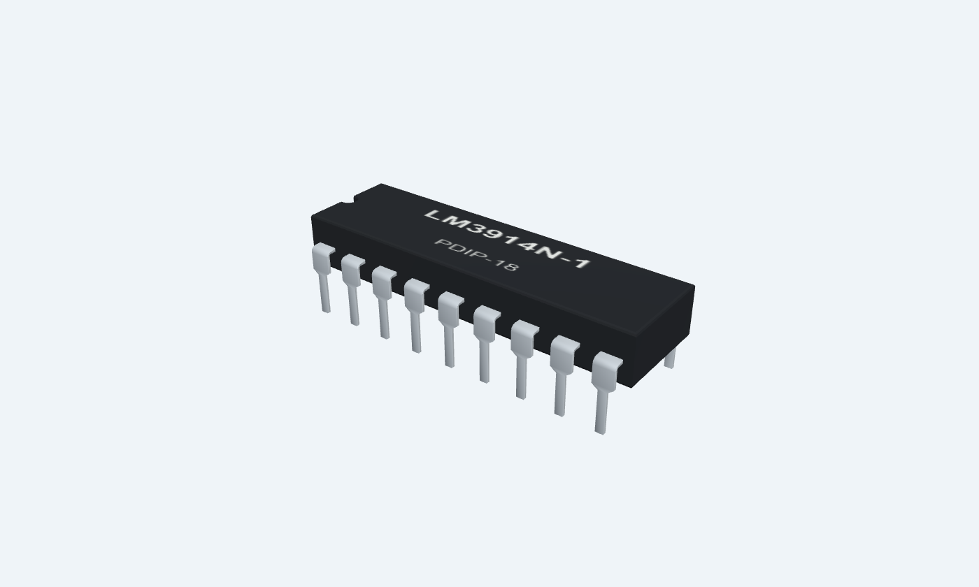
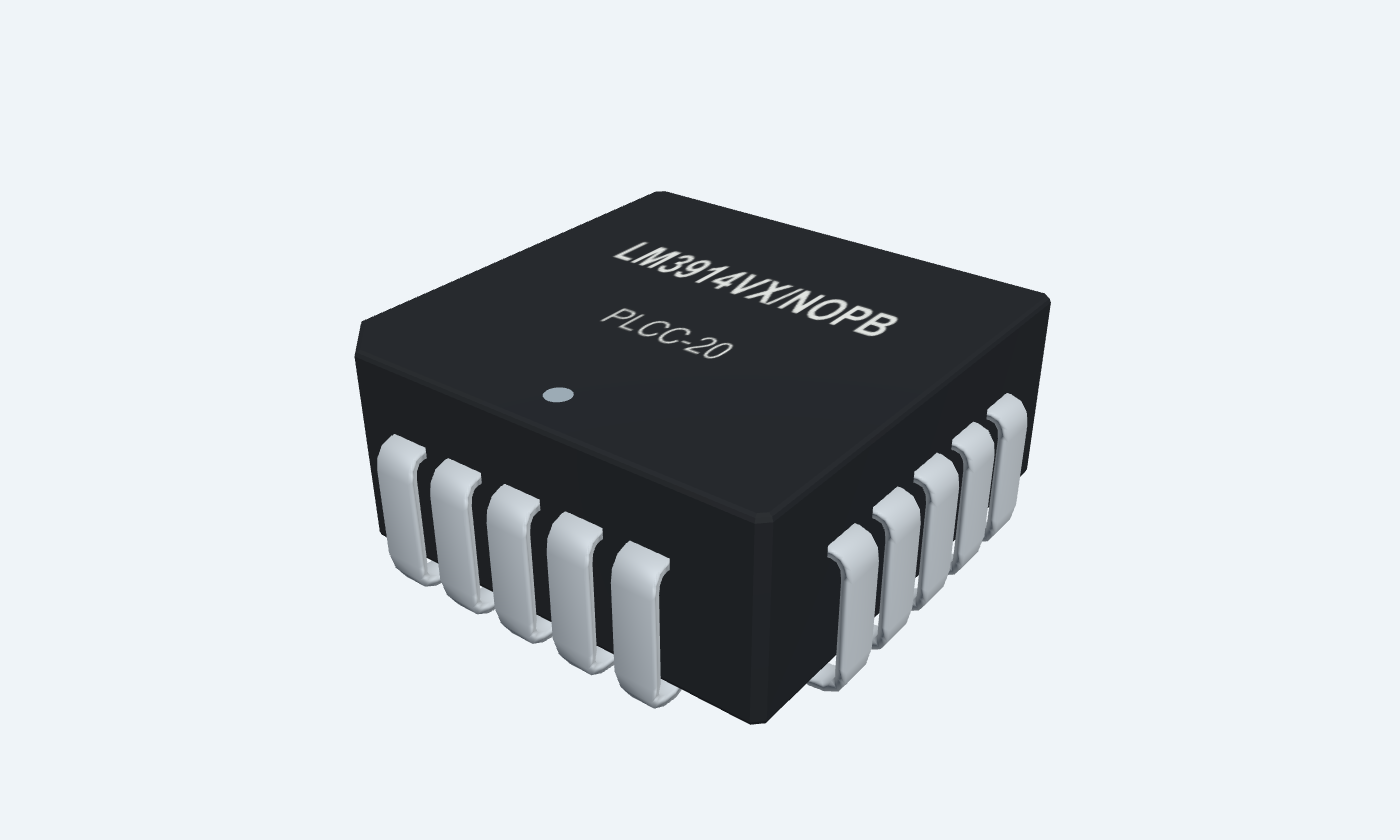
LM3914 converts an analog input into ten evenly spaced display levels. A precision resistor ladder and ten comparators drive regulated LED current sinks, so the LEDs normally do not need individual series resistors. The display can show a single moving dot or a growing bar. The reference network sets the full-scale voltage and influences LED current. This example uses a 5 V supply, a nominal 0–1.25 V signal range and about 6 mA per indicator. The reference is not an exact 1.250 V calibration standard: actual thresholds and current follow the device and resistor tolerances. Package choices matter here: the through-hole LM3914N-1 has 18 pins, while the legacy LM3914VX/NOPB SMD part uses a 20-pin PLCC with two unused contacts and different numbering. The manufacturer lists that PLCC orderable as obsolete. All four views follow the selected package; do not wire it using the DIP pin numbers.

18Physical pins
LM3914N-1PDIP-18
Manufacturer-referencedTexas Instruments
Pin diagram
Select a pin to explore its connection
Highlight
LM3914PDIP-18Top view
LM3914PLCC-20Top view · pin 1 at top center
Click a lead or use the arrow keys. Top view
PIN 1 · LED cathode sinks
Regulated current sinkLED1
Function
Current-regulated cathode driver for indicator 1. Current flows into this pin when active.
How to connect
Connect the LED cathode here and its anode to the positive LED supply.
Electrical note
Check total package dissipation when many LEDs are lit.
PIN 2 · Supply
Supply railV−
Function
Common supply and signal return.
How to connect
Connect to GND.
Electrical note
Use exact package pin mapping; PLCC numbering differs from DIP.
PIN 3 · Supply
Supply railV+
Function
Positive supply for the analog circuitry.
How to connect
Connect to regulated +5 V with local bypass.
Electrical note
Use exact package pin mapping; PLCC numbering differs from DIP.
PIN 4 · Reference and scale
Analog / controlRLO
Function
Bottom of the ten-step resistor ladder.
How to connect
Connect to GND for a zero-based scale.
Electrical note
Use exact package pin mapping; PLCC numbering differs from DIP.
PIN 5 · Signal and mode
Analog / controlSIG
Function
High-impedance measured signal, compared with the ladder taps.
How to connect
Apply a signal between ground and the reference full scale.
Electrical note
Normal measurement input must stay within V+−1.5 V. Protection ratings are not measurement ranges.
PIN 6 · Reference and scale
Analog / controlRHI
Function
Top of the ten-step resistor ladder.
How to connect
Connect to REFOUT in this example.
Electrical note
Use exact package pin mapping; PLCC numbering differs from DIP.
PIN 7 · Reference and scale
Analog / controlREFOUT
Function
Adjustable reference output; loading this pin also programs LED current.
How to connect
Join RHI; connect 2.49 kΩ to GND for approximately 6 mA per LED.
Electrical note
Use exact package pin mapping; PLCC numbering differs from DIP.
PIN 8 · Reference and scale
Analog / controlREFADJ
Function
Reference adjustment return.
How to connect
Connect to GND for the nominal 1.25 V reference.
Electrical note
Use exact package pin mapping; PLCC numbering differs from DIP.
PIN 9 · Signal and mode
Analog / controlMODE
Function
Selects bar or dot display; also supports cascading.
How to connect
Connect to V+ for bar mode. Leave open for the single-chip dot example.
Electrical note
Do not simply ground MODE: pulling it far below the LED supply can disable LED10.
PIN 10 · LED cathode sinks
Regulated current sinkLED10
Function
Current-regulated cathode driver for indicator 10. Current flows into this pin when active.
How to connect
Connect the LED cathode here and its anode to the positive LED supply.
Electrical note
Check total package dissipation when many LEDs are lit.
PIN 11 · LED cathode sinks
Regulated current sinkLED9
Function
Current-regulated cathode driver for indicator 9. Current flows into this pin when active.
How to connect
Connect the LED cathode here and its anode to the positive LED supply.
Electrical note
Check total package dissipation when many LEDs are lit.
PIN 12 · LED cathode sinks
Regulated current sinkLED8
Function
Current-regulated cathode driver for indicator 8. Current flows into this pin when active.
How to connect
Connect the LED cathode here and its anode to the positive LED supply.
Electrical note
Check total package dissipation when many LEDs are lit.
PIN 13 · LED cathode sinks
Regulated current sinkLED7
Function
Current-regulated cathode driver for indicator 7. Current flows into this pin when active.
How to connect
Connect the LED cathode here and its anode to the positive LED supply.
Electrical note
Check total package dissipation when many LEDs are lit.
PIN 14 · LED cathode sinks
Regulated current sinkLED6
Function
Current-regulated cathode driver for indicator 6. Current flows into this pin when active.
How to connect
Connect the LED cathode here and its anode to the positive LED supply.
Electrical note
Check total package dissipation when many LEDs are lit.
PIN 15 · LED cathode sinks
Regulated current sinkLED5
Function
Current-regulated cathode driver for indicator 5. Current flows into this pin when active.
How to connect
Connect the LED cathode here and its anode to the positive LED supply.
Electrical note
Check total package dissipation when many LEDs are lit.
PIN 16 · LED cathode sinks
Regulated current sinkLED4
Function
Current-regulated cathode driver for indicator 4. Current flows into this pin when active.
How to connect
Connect the LED cathode here and its anode to the positive LED supply.
Electrical note
Check total package dissipation when many LEDs are lit.
PIN 17 · LED cathode sinks
Regulated current sinkLED3
Function
Current-regulated cathode driver for indicator 3. Current flows into this pin when active.
How to connect
Connect the LED cathode here and its anode to the positive LED supply.
Electrical note
Check total package dissipation when many LEDs are lit.
PIN 18 · LED cathode sinks
Regulated current sinkLED2
Function
Current-regulated cathode driver for indicator 2. Current flows into this pin when active.
How to connect
Connect the LED cathode here and its anode to the positive LED supply.
Electrical note
Check total package dissipation when many LEDs are lit.
PIN 19 · Not connected
No connectionNC
Function
No internal electrical connection in the PLCC package.
How to connect
Leave unconnected.
PIN 20 · Not connected
No connectionNC
Function
No internal electrical connection in the PLCC package.
How to connect
Leave unconnected.
Key specifications
Turn one analog voltage into a ten-level dot or bar display.
Linear display steps10 Dot or bar
Reference1.28 V typical · specified test
Operating ambient0–70 °C
Programmed LED current2–30 mA feature range
Package details
LM3914N-1 · PDIP-18
| Property | Details |
|---|---|
| Manufacturer | Texas Instruments |
| Part number | LM3914N-1 |
| Package | PDIP-18 |
| Connections | 18 pins |
| Mounting | Through-hole |
| Lead pitch | 2.54 mm |
| Package code | PDIP-18 |
| Thermal reference | See operating and package limits |
Measurement conditions
5 V example; commercial ambient grade
Manufacturer specifications 6 parameters
Scroll sideways to see all columns.
| Parameter | Value | Conditions / notes |
|---|---|---|
| Electrical test supply | 3–20 V | See headroom and power limits; example uses 5 V |
| Ambient | 0–70°C | Commercial parts |
| Normal signal range | 0 to V+−1.5 V | Not the protected overvoltage rating |
| Reference / RHI / RLO headroom | At or below V+−1.5 V | RHI/RLO specified up to12 V |
| Ladder resistance | 12 kΩ typical; 8–17 kΩ | Between RHI and RLO |
| Scale accuracy | 0.5% typical; 2% max | 10 V full scale; offsets matter more at low scales |
No specifications match. Try a parameter name or a unit.
All limits retain their specified conditions. This low-voltage example is illustrative, not a precision instrument.
Reference and current programming
5 V supply, 25°C
Manufacturer specifications 7 parameters
Scroll sideways to see all columns.
| Parameter | Value | Conditions / notes |
|---|---|---|
| Reference output | 1.20–1.34 V; 1.28 V typical | Reference load0.1–4mA |
| REFADJ current | 75 µA typical; 120 µA max | Affects raised-reference calculations |
| LED current scale | Approximately10× reference output load | Include the resistor ladder load |
| Specified LED current | 7–13 mA; 10 mA typical | Reference load1mA, VLED5V |
| Signal bias current | 25 nA typical; 100 nA max | Within normal signal range |
| Offset, first comparator + buffer | 3 mV typical; 10 mV max | Ladder endpoints equal, ILED1mA |
| Other comparator offsets | 3 mV typical; 15 mV max | Same conditions |
No specifications match. Try a parameter name or a unit.
Use measured reference and calibrated scale for accurate instruments.
Nominal 1.25 V bar indicator
PDIP-18 drawing; use pin map for PLCC
Manufacturer specifications 8 parameters
Scroll sideways to see all columns.
| Parameter | Value | Conditions / notes |
|---|---|---|
| V+ / V− | 5 V / GND | DIP3 / DIP2 |
| RLO / REFADJ | Both GND | DIP4 / DIP8 |
| RHI / REFOUT | Joined together | DIP6 / DIP7 |
| Current-setting resistor | 2.49 kΩ from REFOUT to GND | Approximate6mA class; ladder loading increases current |
| MODE | Tie to V+ for bar | DIP9; leave open for dot |
| Input | 0 to nominal1.25 V | DIP5; source referenced toGND |
| LEDs | Anodes5V; cathodesLED1–LED10 | DIP1,18,17,16,15,14,13,12,11,10 |
| Bypass | 100 nF plus10 µF near supply | Local ground; bulk required for long LED leads |
No specifications match. Try a parameter name or a unit.
With1.25V and12kΩ ladder, IREF≈1.25/2490+1.25/12000=0.606mA; ILED≈6.06mA. This includes the ladder current.
Expected bar thresholds
RLO=0; RHI nominal1.25 V
Manufacturer specifications 10 parameters
Scroll sideways to see all columns.
| Parameter | Value | Conditions / notes |
|---|---|---|
| LED1 | 0.125 V | (RHI−RLO)×1/10+RLO |
| LED2 | 0.250 V | (RHI−RLO)×2/10+RLO |
| LED3 | 0.375 V | (RHI−RLO)×3/10+RLO |
| LED4 | 0.500 V | (RHI−RLO)×4/10+RLO |
| LED5 | 0.625 V | (RHI−RLO)×5/10+RLO |
| LED6 | 0.750 V | (RHI−RLO)×6/10+RLO |
| LED7 | 0.875 V | (RHI−RLO)×7/10+RLO |
| LED8 | 1.000 V | (RHI−RLO)×8/10+RLO |
| LED9 | 1.125 V | (RHI−RLO)×9/10+RLO |
| LED10 | 1.250 V | (RHI−RLO)×10/10+RLO |
No specifications match. Try a parameter name or a unit.
Ideal thresholds only. Actual reference, resistor ladder and comparator offset determine switching.
Loading and heat
Keep output dissipation under control
Manufacturer specifications 6 parameters
Scroll sideways to see all columns.
| Parameter | Value | Conditions / notes |
|---|---|---|
| Standby current | 2.4 mA typical; 4.2 mA max | 5 V, IREF0.2mA, outputs off |
| Output dropout | 1.5 V typical | 20mA LED current; stated regulation test |
| Output saturation | 0.15 V typical;0.4V max | 2mA LEDcurrent |
| Bar-mode example dissipation | About0.18W in LED drivers | 10×(5−2)×0.006; plus internal dissipation |
| PDIP thermal reference | 55°C/W junction-to-ambient | Specified package; board-dependent |
| Maximum junction | 100°C | Apply derating at elevated ambient |
No specifications match. Try a parameter name or a unit.
Do not multiply the30mA feature value by ten without checking thermal feasibility.
Dot, bar and cascading
Use the MODE control correctly
Manufacturer specifications 4 parameters
Scroll sideways to see all columns.
| Parameter | Value | Conditions / notes |
|---|---|---|
| Bar | MODE tied to V+ | All outputs up to the selected level light |
| Dot | MODE left open in single-chip use | One nominal indication; transitions can overlap |
| Grounded MODE | Not a generic dot-mode setting | Can disable LED10 when far below the LED rail |
| Cascading | Follow manufacturer circuits | Special full-scale dot carry behavior |
No specifications match. Try a parameter name or a unit.
This example uses bar mode; the LED output numbering runs in the reverse physical order along the DIP right side.
Package and stress limits
LM3914N-1 · PDIP-18
Manufacturer specifications 6 parameters
Scroll sideways to see all columns.
| Parameter | Value | Conditions / notes |
|---|---|---|
| Physical pitch | 2.54 mm | Through-hole |
| Absolute supply / LED voltage | 25 V | Stress limit, not recommended continuous operation |
| Protected signal input | ±35 V | Input current limited to±3mA; not linear measurement range |
| Reference load maximum | 10 mA | Stress rating |
| Storage | −55 to+150°C | Unpowered |
| SMD availability | LM3914VX/NOPB obsolete | TI package addendum; legacy footprint only |
No specifications match. Try a parameter name or a unit.
Observe measurement headroom, current and thermal constraints together.
Connections by function
Select a pin for its function, connection guidance and electrical notes.
LED cathode sinks10 pins
Supply2 pins
Reference and scale4 pins
Signal and mode2 pins
Supply2 pins
LED cathode sinks10 pins
Reference and scale4 pins
Signal and mode2 pins
Not connected2 pins
LM3914 at a glance
Follow the labeled connections and functional stages
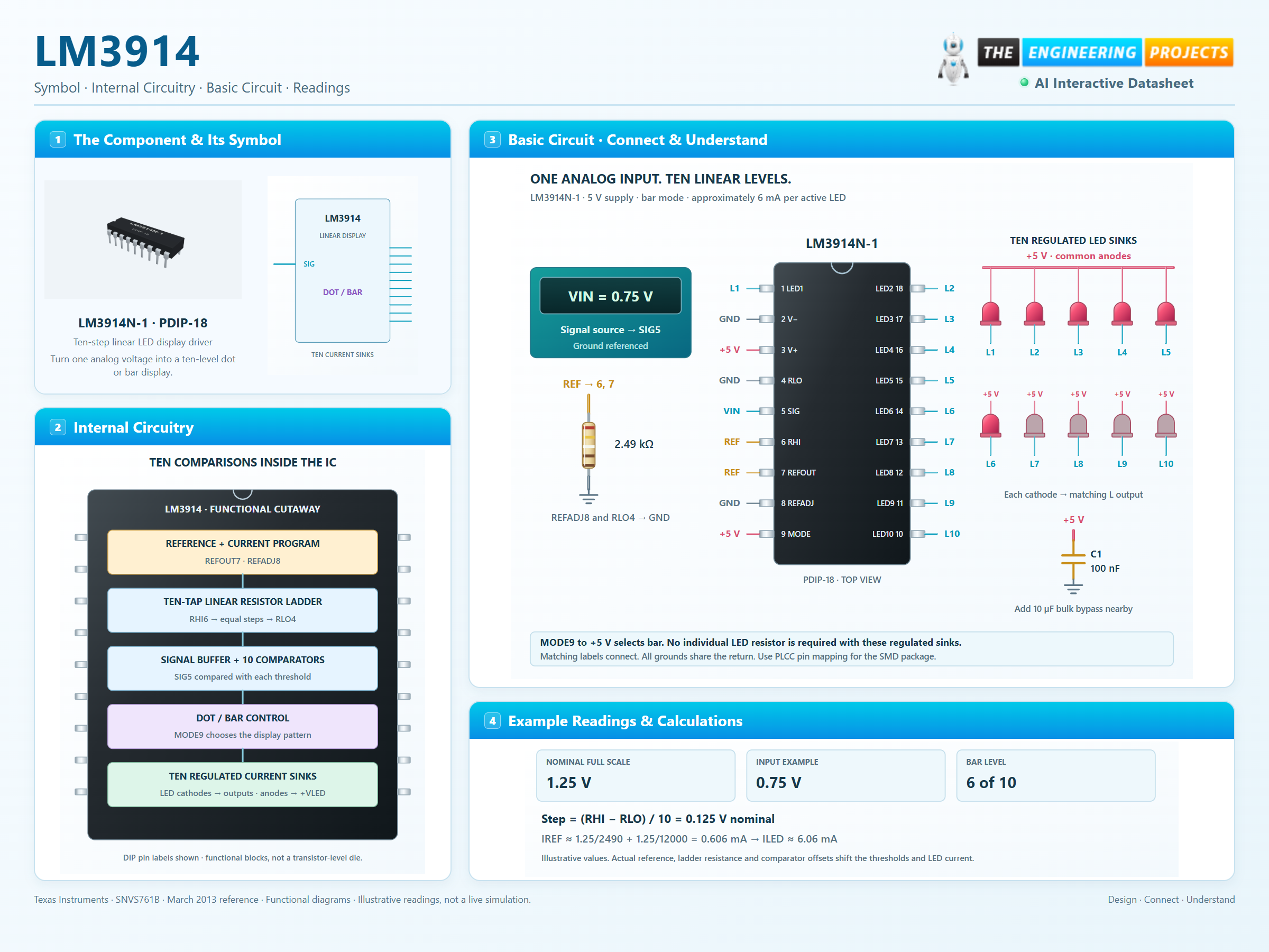
How it works
3 stages · Explore one step at a time
Set the scale
RLO and RHI establish the ten-step comparison range.
Compare the input
The buffer distributes SIG to ten comparators connected to the ladder taps.
Drive the LEDs
Dot/bar logic selects current sinks; the reference load sets approximate brightness.
Step 1 of 3
LM3914 in a circuit
Physical DIP circuit with current-programmed LEDs.
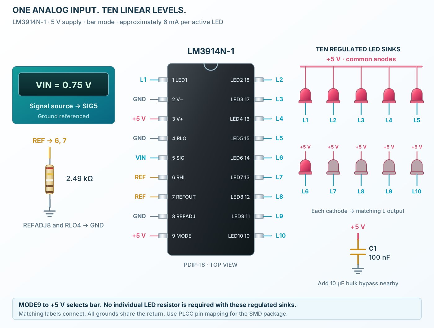
Connect it, step by step
Follow the component values and pin connections
Reference
REFADJ and RLO to GND; join RHI and REFOUT.
Program
Place2.49kΩ from REFOUT toGND; account for ladder load.
Indicate
MODE to5V forbar; ten LED anodes to5V and cathodes to their sinks.
Inside LM3914
Analog comparison and regulated LED sinks.
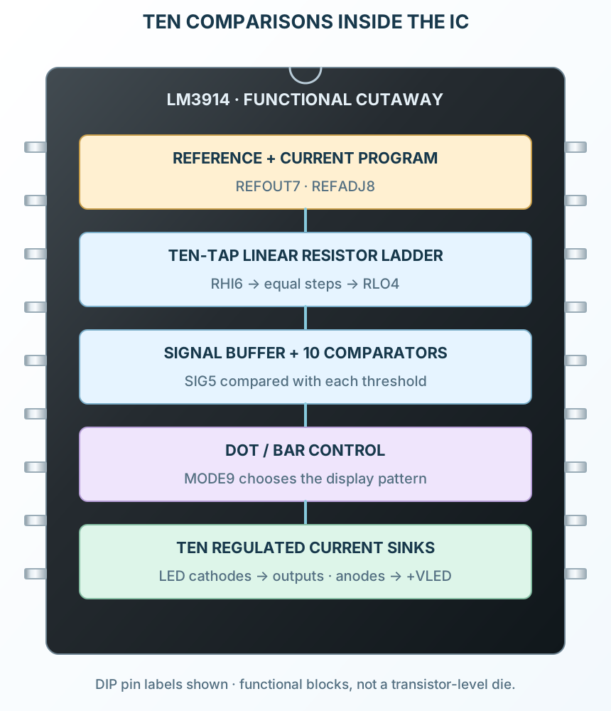
Explore the circuit
Select a stage to see its role and connections
Reference
Set scale and current.
Compare
Ten linear thresholds.
Display
Dot or bar drives regulated cathode sinks.
Selected packagePDIP-18LM3914N-1
Physical connections18 pinsPackage-specific numbering
Reference collection8 tables47 parameters & pin functions
Pin reference
Signal names, electrical functions and connection guidance
Physical pin numbers18 pins
Scroll within the table to see all columns and rows.
| Pin | Signal | Type | Function & connection |
|---|---|---|---|
| LED1 | Regulated current sink | Current-regulated cathode driver for indicator 1. Current flows into this pin when active.Connection guidanceConnect the LED cathode here and its anode to the positive LED supply. Check total package dissipation when many LEDs are lit. | |
| V− | Supply rail | Common supply and signal return.Connection guidanceConnect to GND. Use exact package pin mapping; PLCC numbering differs from DIP. | |
| V+ | Supply rail | Positive supply for the analog circuitry.Connection guidanceConnect to regulated +5 V with local bypass. Use exact package pin mapping; PLCC numbering differs from DIP. | |
| RLO | Analog / control | Bottom of the ten-step resistor ladder.Connection guidanceConnect to GND for a zero-based scale. Use exact package pin mapping; PLCC numbering differs from DIP. | |
| SIG | Analog / control | High-impedance measured signal, compared with the ladder taps.Connection guidanceApply a signal between ground and the reference full scale. Normal measurement input must stay within V+−1.5 V. Protection ratings are not measurement ranges. | |
| RHI | Analog / control | Top of the ten-step resistor ladder.Connection guidanceConnect to REFOUT in this example. Use exact package pin mapping; PLCC numbering differs from DIP. | |
| REFOUT | Analog / control | Adjustable reference output; loading this pin also programs LED current.Connection guidanceJoin RHI; connect 2.49 kΩ to GND for approximately 6 mA per LED. Use exact package pin mapping; PLCC numbering differs from DIP. | |
| REFADJ | Analog / control | Reference adjustment return.Connection guidanceConnect to GND for the nominal 1.25 V reference. Use exact package pin mapping; PLCC numbering differs from DIP. | |
| MODE | Analog / control | Selects bar or dot display; also supports cascading.Connection guidanceConnect to V+ for bar mode. Leave open for the single-chip dot example. Do not simply ground MODE: pulling it far below the LED supply can disable LED10. | |
| LED10 | Regulated current sink | Current-regulated cathode driver for indicator 10. Current flows into this pin when active.Connection guidanceConnect the LED cathode here and its anode to the positive LED supply. Check total package dissipation when many LEDs are lit. | |
| LED9 | Regulated current sink | Current-regulated cathode driver for indicator 9. Current flows into this pin when active.Connection guidanceConnect the LED cathode here and its anode to the positive LED supply. Check total package dissipation when many LEDs are lit. | |
| LED8 | Regulated current sink | Current-regulated cathode driver for indicator 8. Current flows into this pin when active.Connection guidanceConnect the LED cathode here and its anode to the positive LED supply. Check total package dissipation when many LEDs are lit. | |
| LED7 | Regulated current sink | Current-regulated cathode driver for indicator 7. Current flows into this pin when active.Connection guidanceConnect the LED cathode here and its anode to the positive LED supply. Check total package dissipation when many LEDs are lit. | |
| LED6 | Regulated current sink | Current-regulated cathode driver for indicator 6. Current flows into this pin when active.Connection guidanceConnect the LED cathode here and its anode to the positive LED supply. Check total package dissipation when many LEDs are lit. | |
| LED5 | Regulated current sink | Current-regulated cathode driver for indicator 5. Current flows into this pin when active.Connection guidanceConnect the LED cathode here and its anode to the positive LED supply. Check total package dissipation when many LEDs are lit. | |
| LED4 | Regulated current sink | Current-regulated cathode driver for indicator 4. Current flows into this pin when active.Connection guidanceConnect the LED cathode here and its anode to the positive LED supply. Check total package dissipation when many LEDs are lit. | |
| LED3 | Regulated current sink | Current-regulated cathode driver for indicator 3. Current flows into this pin when active.Connection guidanceConnect the LED cathode here and its anode to the positive LED supply. Check total package dissipation when many LEDs are lit. | |
| LED2 | Regulated current sink | Current-regulated cathode driver for indicator 2. Current flows into this pin when active.Connection guidanceConnect the LED cathode here and its anode to the positive LED supply. Check total package dissipation when many LEDs are lit. | |
| NC | No connection | No internal electrical connection in the PLCC package.Connection guidanceLeave unconnected. | |
| NC | No connection | No internal electrical connection in the PLCC package.Connection guidanceLeave unconnected. |
No pins match these filters. Try another signal name or reset the filters.
Measurement conditions
5 V example; commercial ambient grade
Manufacturer-referenced values6 parameters
Scroll within the table to see all columns and rows.
| Parameter | Value | Conditions / notes |
|---|---|---|
| Electrical test supply | 3–20 V | See headroom and power limits; example uses 5 V |
| Ambient | 0–70°C | Commercial parts |
| Normal signal range | 0 to V+−1.5 V | Not the protected overvoltage rating |
| Reference / RHI / RLO headroom | At or below V+−1.5 V | RHI/RLO specified up to12 V |
| Ladder resistance | 12 kΩ typical; 8–17 kΩ | Between RHI and RLO |
| Scale accuracy | 0.5% typical; 2% max | 10 V full scale; offsets matter more at low scales |
No specifications match. Try a parameter name or a unit.
All limits retain their specified conditions. This low-voltage example is illustrative, not a precision instrument.
Reference and current programming
5 V supply, 25°C
Manufacturer-referenced values7 parameters
Scroll within the table to see all columns and rows.
| Parameter | Value | Conditions / notes |
|---|---|---|
| Reference output | 1.20–1.34 V; 1.28 V typical | Reference load0.1–4mA |
| REFADJ current | 75 µA typical; 120 µA max | Affects raised-reference calculations |
| LED current scale | Approximately10× reference output load | Include the resistor ladder load |
| Specified LED current | 7–13 mA; 10 mA typical | Reference load1mA, VLED5V |
| Signal bias current | 25 nA typical; 100 nA max | Within normal signal range |
| Offset, first comparator + buffer | 3 mV typical; 10 mV max | Ladder endpoints equal, ILED1mA |
| Other comparator offsets | 3 mV typical; 15 mV max | Same conditions |
No specifications match. Try a parameter name or a unit.
Use measured reference and calibrated scale for accurate instruments.
Nominal 1.25 V bar indicator
PDIP-18 drawing; use pin map for PLCC
Manufacturer-referenced values8 parameters
Scroll within the table to see all columns and rows.
| Parameter | Value | Conditions / notes |
|---|---|---|
| V+ / V− | 5 V / GND | DIP3 / DIP2 |
| RLO / REFADJ | Both GND | DIP4 / DIP8 |
| RHI / REFOUT | Joined together | DIP6 / DIP7 |
| Current-setting resistor | 2.49 kΩ from REFOUT to GND | Approximate6mA class; ladder loading increases current |
| MODE | Tie to V+ for bar | DIP9; leave open for dot |
| Input | 0 to nominal1.25 V | DIP5; source referenced toGND |
| LEDs | Anodes5V; cathodesLED1–LED10 | DIP1,18,17,16,15,14,13,12,11,10 |
| Bypass | 100 nF plus10 µF near supply | Local ground; bulk required for long LED leads |
No specifications match. Try a parameter name or a unit.
With1.25V and12kΩ ladder, IREF≈1.25/2490+1.25/12000=0.606mA; ILED≈6.06mA. This includes the ladder current.
Expected bar thresholds
RLO=0; RHI nominal1.25 V
Manufacturer-referenced values10 parameters
Scroll within the table to see all columns and rows.
| Parameter | Value | Conditions / notes |
|---|---|---|
| LED1 | 0.125 V | (RHI−RLO)×1/10+RLO |
| LED2 | 0.250 V | (RHI−RLO)×2/10+RLO |
| LED3 | 0.375 V | (RHI−RLO)×3/10+RLO |
| LED4 | 0.500 V | (RHI−RLO)×4/10+RLO |
| LED5 | 0.625 V | (RHI−RLO)×5/10+RLO |
| LED6 | 0.750 V | (RHI−RLO)×6/10+RLO |
| LED7 | 0.875 V | (RHI−RLO)×7/10+RLO |
| LED8 | 1.000 V | (RHI−RLO)×8/10+RLO |
| LED9 | 1.125 V | (RHI−RLO)×9/10+RLO |
| LED10 | 1.250 V | (RHI−RLO)×10/10+RLO |
No specifications match. Try a parameter name or a unit.
Ideal thresholds only. Actual reference, resistor ladder and comparator offset determine switching.
Loading and heat
Keep output dissipation under control
Manufacturer-referenced values6 parameters
Scroll within the table to see all columns and rows.
| Parameter | Value | Conditions / notes |
|---|---|---|
| Standby current | 2.4 mA typical; 4.2 mA max | 5 V, IREF0.2mA, outputs off |
| Output dropout | 1.5 V typical | 20mA LED current; stated regulation test |
| Output saturation | 0.15 V typical;0.4V max | 2mA LEDcurrent |
| Bar-mode example dissipation | About0.18W in LED drivers | 10×(5−2)×0.006; plus internal dissipation |
| PDIP thermal reference | 55°C/W junction-to-ambient | Specified package; board-dependent |
| Maximum junction | 100°C | Apply derating at elevated ambient |
No specifications match. Try a parameter name or a unit.
Do not multiply the30mA feature value by ten without checking thermal feasibility.
Dot, bar and cascading
Use the MODE control correctly
Manufacturer-referenced values4 parameters
Scroll within the table to see all columns and rows.
| Parameter | Value | Conditions / notes |
|---|---|---|
| Bar | MODE tied to V+ | All outputs up to the selected level light |
| Dot | MODE left open in single-chip use | One nominal indication; transitions can overlap |
| Grounded MODE | Not a generic dot-mode setting | Can disable LED10 when far below the LED rail |
| Cascading | Follow manufacturer circuits | Special full-scale dot carry behavior |
No specifications match. Try a parameter name or a unit.
This example uses bar mode; the LED output numbering runs in the reverse physical order along the DIP right side.
Package and stress limits
LM3914N-1 · PDIP-18
Manufacturer-referenced values6 parameters
Scroll within the table to see all columns and rows.
| Parameter | Value | Conditions / notes |
|---|---|---|
| Physical pitch | 2.54 mm | Through-hole |
| Absolute supply / LED voltage | 25 V | Stress limit, not recommended continuous operation |
| Protected signal input | ±35 V | Input current limited to±3mA; not linear measurement range |
| Reference load maximum | 10 mA | Stress rating |
| Storage | −55 to+150°C | Unpowered |
| SMD availability | LM3914VX/NOPB obsolete | TI package addendum; legacy footprint only |
No specifications match. Try a parameter name or a unit.
Observe measurement headroom, current and thermal constraints together.
No matching rowsTry a pin name, parameter, unit or test condition, or reset the filters.
Voltage indicators
Display a bounded sensor or supply measurement with suitable input scaling.
Manufacturer application guideLevel meters
Show a linear analog level after signal conditioning.
Manufacturer application guidePanel instruments
Use calibrated references and thermal design for practical indicators.
Manufacturer application guideTake it into ProTech
Find LM3914 in the Components Library to place its schematic symbol and connect its pins.
Reference page · circuit simulation model not yet availableOpen ProTech