Real View
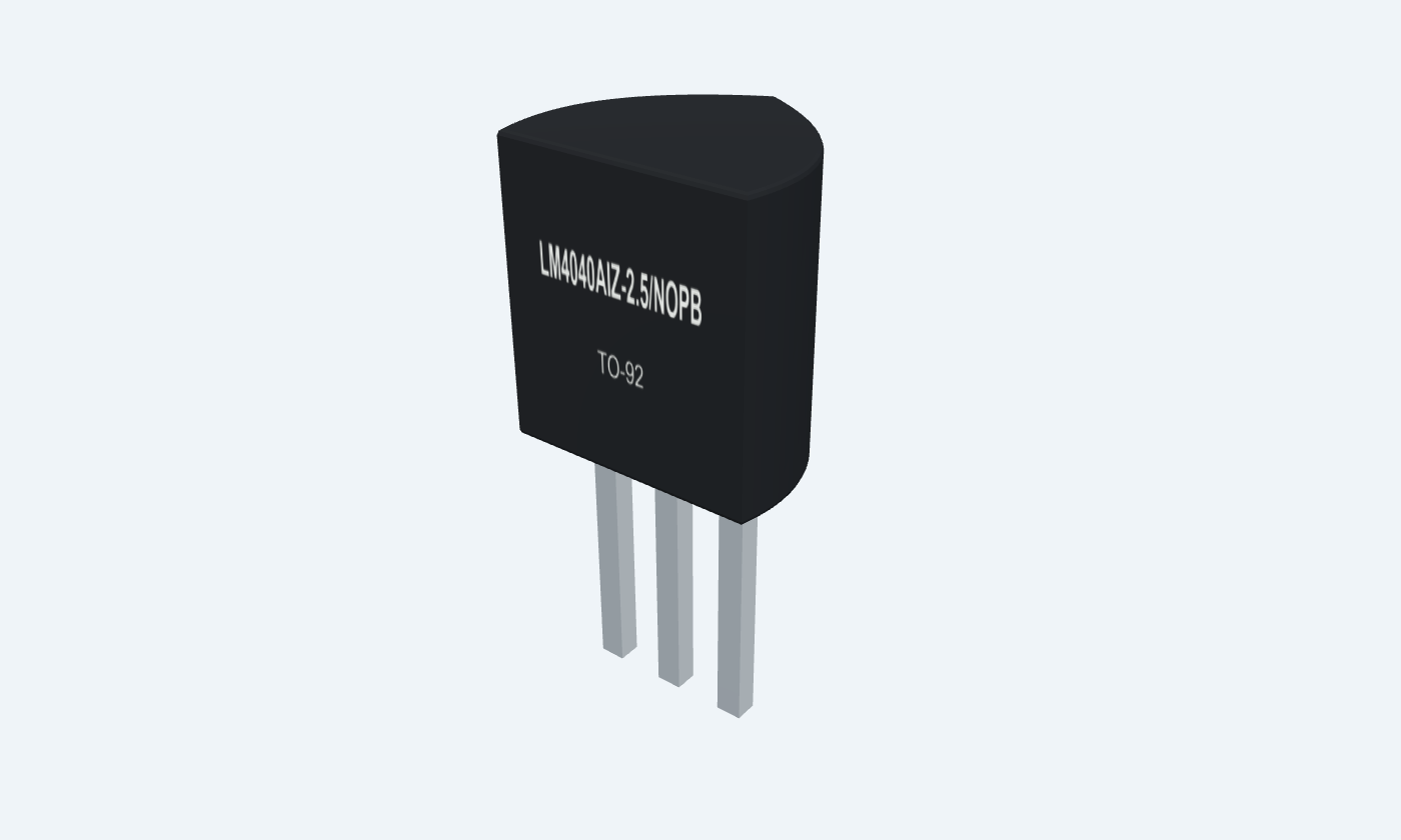
A precise voltage reference with just two active connections.
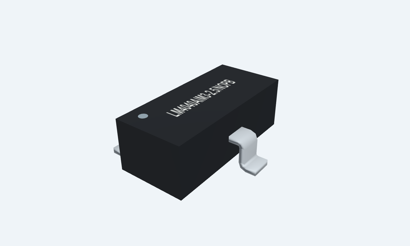
LM4040 is a fixed shunt voltage-reference family. This page selects the A-grade 2.5 V industrial version: it holds the cathode near 2.5 V relative to the anode by sinking current supplied through an external resistor. It is a precision reference, not a power-supply regulator. The selected LM4040AIZ-2.5/NOPB in TO-92 and LM4040AIM3-2.5/NOPB in SOT-23 have different physical pin numbers. Both have only two active electrical connections; the third lead must float or connect to the anode. All package views and footprint downloads follow the selected version. Initial accuracy is ±0.1% at 25°C and 100 µA reference current. The industrial ambient range is −40 to 85°C. Budget at least 65 µA reference current for the full temperature range, stay below 15 mA in normal use, and account for load current and temperature drift.
Select a pin to explore its connection
Click a lead or use the arrow keys. Front view · flat face toward you · 1 DNC, 2 K, 3 A
This package lead must not be used as an input or output.
Leave floating in the example. TI also permits an anode connection and recommends it in noisy environments.
TO-92 pin 1; SOT-23 pin 3. No adjustment function.
Positive shunt-current terminal and nominal 2.5 V output.
Feed through a resistor from the source; connect a high-impedance load to this node.
TO-92 pin 2; SOT-23 pin 1. Keep reference current within its operating range.
Negative reference terminal, normally grounded.
Connect to supply return and the measurement ground.
TO-92 pin 3; SOT-23 pin 2.
A series resistor supplies both the external load and the shunt reference. If the load takes too much current, the reference falls out of regulation.
LM4040AIZ-2.5/NOPB · TO-92
| Property | Details |
|---|---|
| Manufacturer | Texas Instruments |
| Part number | LM4040AIZ-2.5/NOPB |
| Package | TO-92 |
| Connections | 3 pins |
| Mounting | Through-hole |
| Lead pitch | 1.27 mm · straight leads |
| Package code | LP |
| Thermal reference | θJA 166°C/W under TI reference conditions; mounting dependent |
A-grade 2.5 V industrial devices
Scroll sideways to see all columns.
| Parameter | Value | Conditions / notes |
|---|---|---|
| Through-hole order | LM4040AIZ-2.5/NOPB | TO-92 LP; straight leads |
| SMD order | LM4040AIM3-2.5/NOPB | SOT-23 DBZ; body code R2A |
| TO-92 front-view pins | 1 DNC; 2 cathode; 3 anode | Flat face toward viewer |
| SOT-23 top-view pins | 1 cathode; 2 anode; 3 DNC | DNC must float or connect to anode |
| Active terminals | Cathode and anode | No adjustment or enable input |
| Selected accuracy / temperature | A grade / I range | Not C, D, E or automotive limits |
No specifications match. Try a parameter name or a unit.
The TO-92 manufacturer drawing is a bottom view; the page labels its viewing orientation.
IR=100 µA unless noted
Scroll sideways to see all columns.
| Parameter | Value | Conditions / notes |
|---|---|---|
| Nominal breakdown voltage | 2.5 V | Reverse operation |
| Initial A-grade error | ±2.5 mV maximum | ±0.1%; 25°C |
| Full-temperature A-grade error | ±19 mV maximum | −40 to 85°C; 2.481–2.519 V |
| Average temperature coefficient | ±100 ppm/°C maximum | Full specified temperature span |
| Typical temperature coefficient | ±15 ppm/°C | 100 µA or 1 mA |
| Typical coefficient at 10 mA | ±20 ppm/°C | Characterization, not a maximum |
No specifications match. Try a parameter name or a unit.
Initial accuracy is not the complete overtemperature error.
Preserve current for both load and reference
Scroll sideways to see all columns.
| Parameter | Value | Conditions / notes |
|---|---|---|
| Minimum operating current at 25°C | 45 µA typical; 60 µA maximum | Use the maximum requirement for design |
| Minimum over full temperature | 65 µA maximum | Reference current after subtracting load |
| Maximum operating reverse current | 15 mA | Respect package heating |
| Reverse-current absolute maximum | 20 mA | Stress only |
| Forward-current absolute maximum | 10 mA | Not normal reference operation |
| Dynamic impedance | 0.3 Ω typical; 0.8 Ω maximum | IR1 mA, 120 Hz, AC current 10% of IR |
No specifications match. Try a parameter name or a unit.
A shunt reference draws the current left over by the load.
Source test conditions retained
Scroll sideways to see all columns.
| Parameter | Value | Conditions / notes |
|---|---|---|
| Voltage change: IRmin to 1 mA | 0.3 mV typ.; 0.8 mV max. at 25°C | 1 mV maximum over temperature |
| Voltage change: 1–15 mA | 2.5 mV typ.; 6 mV max. at 25°C | 8 mV maximum over temperature |
| Wideband noise | 35 µV RMS typical | IR100 µA, 10 Hz–10 kHz |
| Long-term stability | 120 ppm typical | 1000 h; 25°C±0.1°C; IR100 µA |
| Thermal hysteresis | 0.08% typical | Manufacturer −40 to125°C cycle test |
| External stabilization capacitor | Not required | Capacitive loads tolerated; system filtering may still help |
No specifications match. Try a parameter name or a unit.
Typical noise and aging figures are not guaranteed maximum errors.
Calculated example, not a power regulator
Scroll sideways to see all columns.
| Parameter | Value | Conditions / notes |
|---|---|---|
| Feed resistor | 2.49 kΩ, 1%, ≥0.25 W | From 5 V source to cathode |
| Test load | 10 kΩ, 1%, ≥0.25 W | From cathode to anode/ground |
| Nominal feed current | (5−2.5)/2490=1.004 mA | Supplies load plus reference |
| Nominal load current | 2.5/10000=250 µA | 0.625 mW load power |
| Nominal reference current | 754 µA | 1.004 mA−250 µA |
| Nominal reference dissipation | 2.5×0.754 mA≈1.89 mW | Feed resistor dissipates approximately 2.51 mW |
| Worst-case low-source budget | At 4.75 V, VR2.519 V, RS+1%, RL−1%: IR≈633 µA | Still above 65 µA before additional system loads |
No specifications match. Try a parameter name or a unit.
A high-impedance measurement input is preferable to a heavy load.
Board-dependent thermal metrics
Scroll sideways to see all columns.
| Parameter | Value | Conditions / notes |
|---|---|---|
| Ambient operating range | −40 to85°C | Selected industrial temperature grade |
| Maximum junction temperature | 125°C | Use the operating and power-derating guidance |
| TO-92 θJA | 166°C/W | TI thermal-information reference board |
| SOT-23 θJA | 291.9°C/W | TI thermal-information reference board |
| Reference loss at 15 mA | 37.5 mW nominal | 2.5 V×15 mA |
| Layout | Short reference and return paths | Keep load-return drops out of sensitive measurements |
No specifications match. Try a parameter name or a unit.
Thermal resistance depends on assembly; older lead-length estimates are not interchangeable with reference-board metrics.
Select a pin for its function, connection guidance and electrical notes.
Follow the labeled connections and functional stages
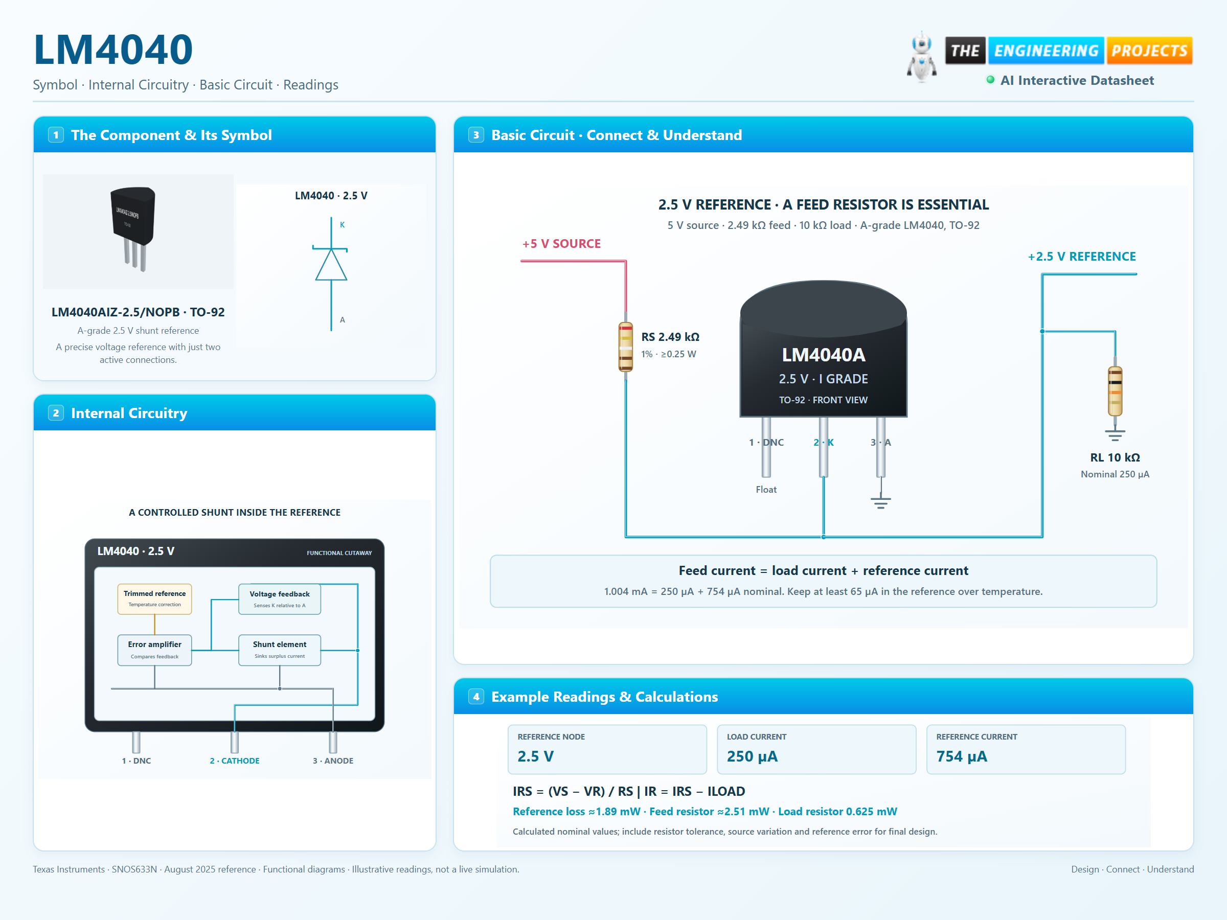
3 stages · Explore one step at a time
Always use a feed resistor or a controlled current source. Never connect the shunt directly across 5 V.
Subtract the maximum load current from the minimum feed current; retain at least 65 µA over temperature.
A-grade, 2.5 V and industrial I-temperature limits are used here; other grades differ.
TO-92 physical connections, feed resistor and a modest load.
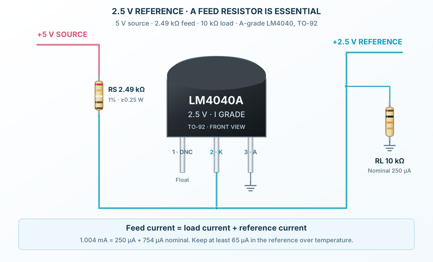
Follow the component values and pin connections
Use 2.49 kΩ from 5 V to cathode2.
Ground anode3; leave DNC1 floating in this example.
A 10 kΩ load leaves approximately 754 µA reference current at nominal values.
A compact feedback-controlled current path between cathode and anode.
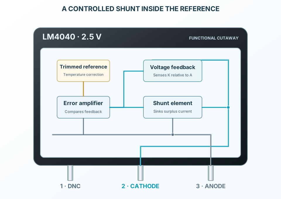
Select a stage to see its role and connections
Monitor cathode voltage relative to the anode.
Compare feedback with the internal trimmed reference.
Vary sink current through the shunt element to hold the reference node.
Signal names, electrical functions and connection guidance
Scroll within the table to see all columns and rows.
| Pin | Signal | Type | Function & connection |
|---|---|---|---|
| DNC | Float or connect to anode | This package lead must not be used as an input or output.Connection guidanceLeave floating in the example. TI also permits an anode connection and recommends it in noisy environments. TO-92 pin 1; SOT-23 pin 3. No adjustment function. | |
| K | Cathode / reference node | Positive shunt-current terminal and nominal 2.5 V output.Connection guidanceFeed through a resistor from the source; connect a high-impedance load to this node. TO-92 pin 2; SOT-23 pin 1. Keep reference current within its operating range. | |
| A | Anode / common return | Negative reference terminal, normally grounded.Connection guidanceConnect to supply return and the measurement ground. TO-92 pin 3; SOT-23 pin 2. |
No pins match these filters. Try another signal name or reset the filters.
A-grade 2.5 V industrial devices
Scroll within the table to see all columns and rows.
| Parameter | Value | Conditions / notes |
|---|---|---|
| Through-hole order | LM4040AIZ-2.5/NOPB | TO-92 LP; straight leads |
| SMD order | LM4040AIM3-2.5/NOPB | SOT-23 DBZ; body code R2A |
| TO-92 front-view pins | 1 DNC; 2 cathode; 3 anode | Flat face toward viewer |
| SOT-23 top-view pins | 1 cathode; 2 anode; 3 DNC | DNC must float or connect to anode |
| Active terminals | Cathode and anode | No adjustment or enable input |
| Selected accuracy / temperature | A grade / I range | Not C, D, E or automotive limits |
No specifications match. Try a parameter name or a unit.
The TO-92 manufacturer drawing is a bottom view; the page labels its viewing orientation.
IR=100 µA unless noted
Scroll within the table to see all columns and rows.
| Parameter | Value | Conditions / notes |
|---|---|---|
| Nominal breakdown voltage | 2.5 V | Reverse operation |
| Initial A-grade error | ±2.5 mV maximum | ±0.1%; 25°C |
| Full-temperature A-grade error | ±19 mV maximum | −40 to 85°C; 2.481–2.519 V |
| Average temperature coefficient | ±100 ppm/°C maximum | Full specified temperature span |
| Typical temperature coefficient | ±15 ppm/°C | 100 µA or 1 mA |
| Typical coefficient at 10 mA | ±20 ppm/°C | Characterization, not a maximum |
No specifications match. Try a parameter name or a unit.
Initial accuracy is not the complete overtemperature error.
Preserve current for both load and reference
Scroll within the table to see all columns and rows.
| Parameter | Value | Conditions / notes |
|---|---|---|
| Minimum operating current at 25°C | 45 µA typical; 60 µA maximum | Use the maximum requirement for design |
| Minimum over full temperature | 65 µA maximum | Reference current after subtracting load |
| Maximum operating reverse current | 15 mA | Respect package heating |
| Reverse-current absolute maximum | 20 mA | Stress only |
| Forward-current absolute maximum | 10 mA | Not normal reference operation |
| Dynamic impedance | 0.3 Ω typical; 0.8 Ω maximum | IR1 mA, 120 Hz, AC current 10% of IR |
No specifications match. Try a parameter name or a unit.
A shunt reference draws the current left over by the load.
Source test conditions retained
Scroll within the table to see all columns and rows.
| Parameter | Value | Conditions / notes |
|---|---|---|
| Voltage change: IRmin to 1 mA | 0.3 mV typ.; 0.8 mV max. at 25°C | 1 mV maximum over temperature |
| Voltage change: 1–15 mA | 2.5 mV typ.; 6 mV max. at 25°C | 8 mV maximum over temperature |
| Wideband noise | 35 µV RMS typical | IR100 µA, 10 Hz–10 kHz |
| Long-term stability | 120 ppm typical | 1000 h; 25°C±0.1°C; IR100 µA |
| Thermal hysteresis | 0.08% typical | Manufacturer −40 to125°C cycle test |
| External stabilization capacitor | Not required | Capacitive loads tolerated; system filtering may still help |
No specifications match. Try a parameter name or a unit.
Typical noise and aging figures are not guaranteed maximum errors.
Calculated example, not a power regulator
Scroll within the table to see all columns and rows.
| Parameter | Value | Conditions / notes |
|---|---|---|
| Feed resistor | 2.49 kΩ, 1%, ≥0.25 W | From 5 V source to cathode |
| Test load | 10 kΩ, 1%, ≥0.25 W | From cathode to anode/ground |
| Nominal feed current | (5−2.5)/2490=1.004 mA | Supplies load plus reference |
| Nominal load current | 2.5/10000=250 µA | 0.625 mW load power |
| Nominal reference current | 754 µA | 1.004 mA−250 µA |
| Nominal reference dissipation | 2.5×0.754 mA≈1.89 mW | Feed resistor dissipates approximately 2.51 mW |
| Worst-case low-source budget | At 4.75 V, VR2.519 V, RS+1%, RL−1%: IR≈633 µA | Still above 65 µA before additional system loads |
No specifications match. Try a parameter name or a unit.
A high-impedance measurement input is preferable to a heavy load.
Board-dependent thermal metrics
Scroll within the table to see all columns and rows.
| Parameter | Value | Conditions / notes |
|---|---|---|
| Ambient operating range | −40 to85°C | Selected industrial temperature grade |
| Maximum junction temperature | 125°C | Use the operating and power-derating guidance |
| TO-92 θJA | 166°C/W | TI thermal-information reference board |
| SOT-23 θJA | 291.9°C/W | TI thermal-information reference board |
| Reference loss at 15 mA | 37.5 mW nominal | 2.5 V×15 mA |
| Layout | Short reference and return paths | Keep load-return drops out of sensitive measurements |
No specifications match. Try a parameter name or a unit.
Thermal resistance depends on assembly; older lead-length estimates are not interchangeable with reference-board metrics.
No matching rowsTry a pin name, parameter, unit or test condition, or reset the filters.
Provide a stable voltage when the ADC input and reference-load requirements are compatible.
Manufacturer application guideUse the reference with a suitably designed high-impedance divider or comparator input.
Manufacturer application guideBudget noise, drift and loading for a repeatable analog reference.
Manufacturer application guideFind LM4040 in the Components Library to place its schematic symbol and connect its pins.
Reference page · circuit simulation model not yet availableOpen ProTech