LM723Adjustable precision regulator
Set the output voltage and current limit with external resistors.
LM723 combines a voltage reference, error amplifier, internal series pass transistor and adjustable current-limit circuit. External resistors determine the regulated output rather than a fixed internal voltage setting. This page covers the commercial LM723C grade in ST’s DIP14 and SO14 packages. The reference is nominally 7.15 V. For a lower output, divide that reference before applying it to the non-inverting input and feed the regulated output back to the inverting input. The pass-stage collector and control-circuit supply are separate pins; both must be connected correctly. The example uses a 12 V input and an approximately 5 V output, with a 10 Ω current-sense resistor and a small 1 kΩ load. All unused contacts remain unconnected. The published ST reference is an archived manufacturer document; check availability and the exact package before sourcing a legacy part.
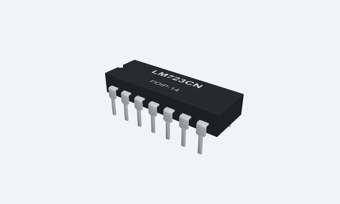
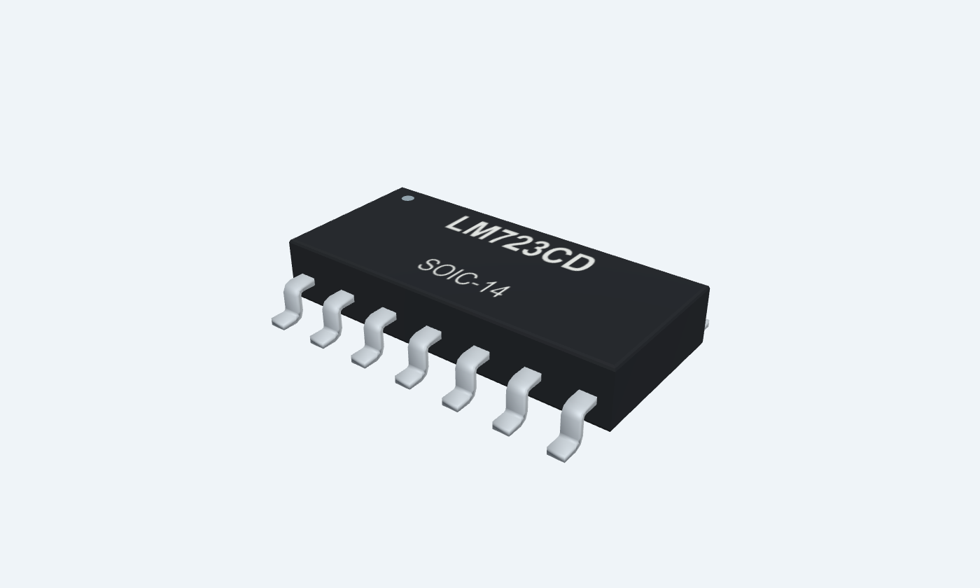

14Physical pins
LM723CNPDIP-14
Manufacturer-referencedSTMicroelectronics
Pin diagram
Select a pin to explore its connection
Highlight
LM723CNPDIP-14Top view
LM723CDSOIC-14Top view
Click a lead or use the arrow keys. Top view
PIN 1 · Not connected
No connectionNC
Function
Unused contact
How to connect
Leave unconnected.
PIN 2 · Control
Input / controlCL
Function
Current-limit transistor base
How to connect
Connect to OUT10 before the 10 Ω sense resistor.
PIN 3 · Control
Input / controlCS
Function
Current-sense transistor emitter
How to connect
Connect to the regulated output after the sense resistor.
PIN 4 · Inputs
Input / controlIN−
Function
Error amplifier feedback
How to connect
Connect to the regulated output through 3 kΩ; connect compensation capacitor here.
PIN 5 · Inputs
Input / controlIN+
Function
Error amplifier reference input
How to connect
Connect to the 4.3 kΩ / 10 kΩ reference-divider junction.
PIN 6 · Reference
Input / controlVREF
Function
Nominal 7.15 V reference
How to connect
Connect 4.3 kΩ to IN+5; 10 kΩ from IN+5 to ground.
PIN 7 · Supply
SupplyV−
Function
Control-circuit return
How to connect
Connect to ground.
PIN 8 · Not connected
No connectionNC
Function
Unused contact
How to connect
Leave unconnected.
PIN 9 · Reference
Input / controlVZ
Function
Internal zener connection
How to connect
Leave open in this positive-output example.
PIN 10 · Outputs
OutputOUT
Function
Internal pass emitter
How to connect
Connect CL2 and the input side of the 10 Ω sense resistor.
PIN 11 · Supply
SupplyVC
Function
Pass-transistor collector
How to connect
Connect to +12 V.
PIN 12 · Supply
SupplyV+
Function
Control-circuit positive supply
How to connect
Connect to +12 V; bypass locally to ground.
PIN 13 · Control
Input / controlCOMP
Function
Frequency compensation
How to connect
Connect 100 pF between COMP13 and IN−4.
PIN 14 · Not connected
No connectionNC
Function
Unused contact
How to connect
Leave unconnected.
Key specifications
Set the output voltage and current limit with external resistors.
Supply9.5–40 V
Output range2–37 V · circuit dependent
Commercial ambient0–70 °C
Reference7.15 V typical
Package details
LM723CN · PDIP-14
| Property | Details |
|---|---|
| Manufacturer | STMicroelectronics |
| Part number | LM723CN |
| Package | PDIP-14 |
| Connections | 14 pins |
| Mounting | Through-hole |
| Lead pitch | 2.54 mm |
| Package code | PDIP-14 |
| Thermal reference | See operating and package limits |
Operating reference
ST LM723C selected grade
Manufacturer specifications 5 parameters
Scroll sideways to see all columns.
| Parameter | Value | Conditions / notes |
|---|---|---|
| Supply range | 9.5–40 V | Maintain input/output headroom |
| Output range | 2–37 V | Appropriate external circuit required |
| Ambient | 0–70°C | LM723C; not extended-grade LM723 |
| Reference | 6.8–7.5 V; 7.15 V typical | IREF = 160 µA |
| Internal output capability | Up to 150 mA | Package dissipation and headroom limit actual use |
No specifications match. Try a parameter name or a unit.
Do not substitute extended-grade limits for the commercial parts.
Regulation and reference
25°C, manufacturer test circuit
Manufacturer specifications 6 parameters
Scroll sideways to see all columns.
| Parameter | Value | Conditions / notes |
|---|---|---|
| Line regulation | 0.01% typical; 0.1% max | 12–15 V input |
| Wide-range line regulation | 0.1% typical; 0.5% max | 12–40 V input |
| Load regulation | 0.03% typical; 0.2% max | 1–50 mA |
| Quiescent current | 2.3 mA typical; 4 mA max | 30 V input; no load |
| Ripple rejection | 74 dB typical | 100 Hz–10 kHz; no reference bypass |
| Current limit | 65 mA typical | RSC = 10 Ω; output shorted |
No specifications match. Try a parameter name or a unit.
Regulation values exclude changing junction temperature.
Five-volt circuit
Nominal calculation
Manufacturer specifications 7 parameters
Scroll sideways to see all columns.
| Parameter | Value | Conditions / notes |
|---|---|---|
| Input | 12 V | V+12 and VC11 |
| Reference divider | 4.3 kΩ / 10 kΩ | VREF6 → 4.3k → IN+5 → 10k → GND |
| Nominal output | 7.15 × 10 / 14.3 = 5 V | Reference and resistor tolerances remain |
| Current sense | 10 Ω | OUT10/CL2 → resistor → regulated output/CS3 |
| Feedback | 3 kΩ to IN−4 | From the regulated output |
| Compensation | 100 pF | COMP13 to IN−4 |
| Load | 1 kΩ | About 5 mA and 25 mW |
No specifications match. Try a parameter name or a unit.
No external pass transistor is needed for this small example.
Thermal and stress limits
LM723CN · PDIP-14
Manufacturer specifications 6 parameters
Scroll sideways to see all columns.
| Parameter | Value | Conditions / notes |
|---|---|---|
| Lead pitch | 2.54 mm | Through-hole |
| Input stress ceiling | 40 V | Do not exceed |
| Reference output stress current | 25 mA | LM723C absolute maximum; avoid designing at it |
| Maximum junction | 125°C | Selected commercial grade |
| θJA reference | 200°C/W DIP; 160°C/W SO14 | Manufacturer reference mounting |
| Storage | −65 to +150°C | Unpowered |
No specifications match. Try a parameter name or a unit.
A headline current limit does not remove the package power limit.
External connections
Physical package contacts
Manufacturer specifications 14 parameters
Scroll sideways to see all columns.
| Parameter | Value | Conditions / notes |
|---|---|---|
| 1 · NC | Unused contact | Leave unconnected. |
| 2 · CL | Current-limit transistor base | Connect to OUT10 before the 10 Ω sense resistor. |
| 3 · CS | Current-sense transistor emitter | Connect to the regulated output after the sense resistor. |
| 4 · IN− | Error amplifier feedback | Connect to the regulated output through 3 kΩ; connect compensation capacitor here. |
| 5 · IN+ | Error amplifier reference input | Connect to the 4.3 kΩ / 10 kΩ reference-divider junction. |
| 6 · VREF | Nominal 7.15 V reference | Connect 4.3 kΩ to IN+5; 10 kΩ from IN+5 to ground. |
| 7 · V− | Control-circuit return | Connect to ground. |
| 8 · NC | Unused contact | Leave unconnected. |
| 9 · VZ | Internal zener connection | Leave open in this positive-output example. |
| 10 · OUT | Internal pass emitter | Connect CL2 and the input side of the 10 Ω sense resistor. |
| 11 · VC | Pass-transistor collector | Connect to +12 V. |
| 12 · V+ | Control-circuit positive supply | Connect to +12 V; bypass locally to ground. |
| 13 · COMP | Frequency compensation | Connect 100 pF between COMP13 and IN−4. |
| 14 · NC | Unused contact | Leave unconnected. |
No specifications match. Try a parameter name or a unit.
Connect all supply and return contacts; leave only explicitly unused contacts open.
Connections by function
Select a pin for its function, connection guidance and electrical notes.
Not connected3 pins
Control3 pins
Inputs2 pins
Reference2 pins
Supply3 pins
Outputs1 pin
Not connected3 pins
Control3 pins
Inputs2 pins
Reference2 pins
Supply3 pins
Outputs1 pin
LM723 at a glance
Follow the labeled connections and functional stages
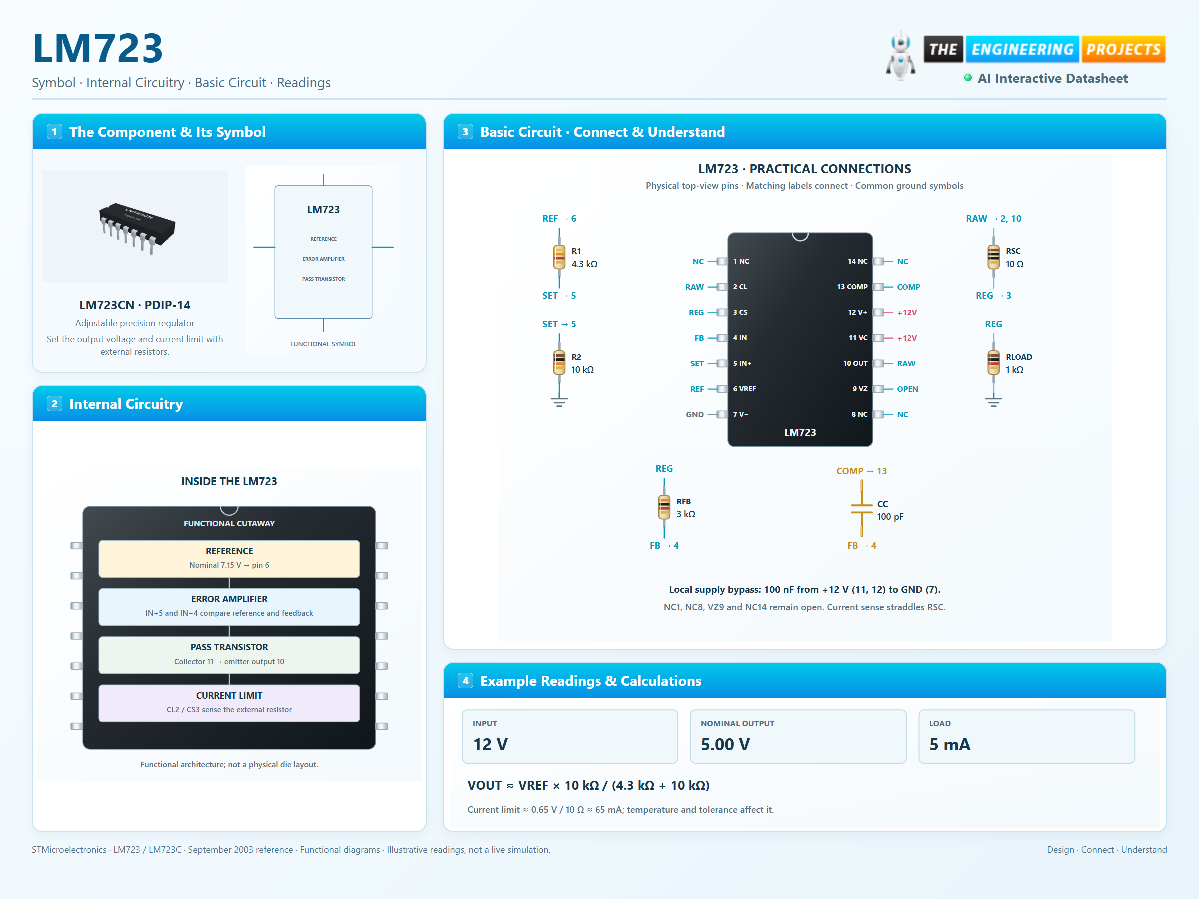
How it works
3 stages · Explore one step at a time
Input and reference
Divide the reference to the intended output level.
Internal control
Compare that level against the sensed regulated output.
Output behavior
Adjust pass current; the sense resistor activates current limiting.
Step 1 of 3
LM723 in a circuit
Physical package with colored wiring and explicit node labels.
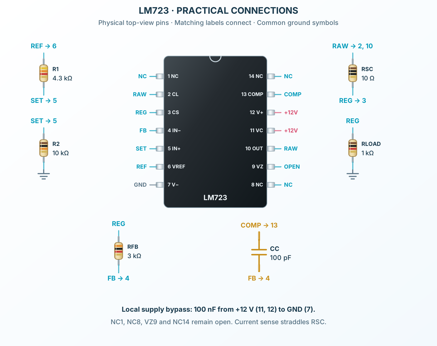
Connect it, step by step
Follow the component values and pin connections
Power
Connect every specified supply and return contact.
External network
Fit the external components at the numbered pins shown.
Check
Compare the nominal calculation with device and component tolerances.
Inside LM723
Compact functional stages inside the IC body.
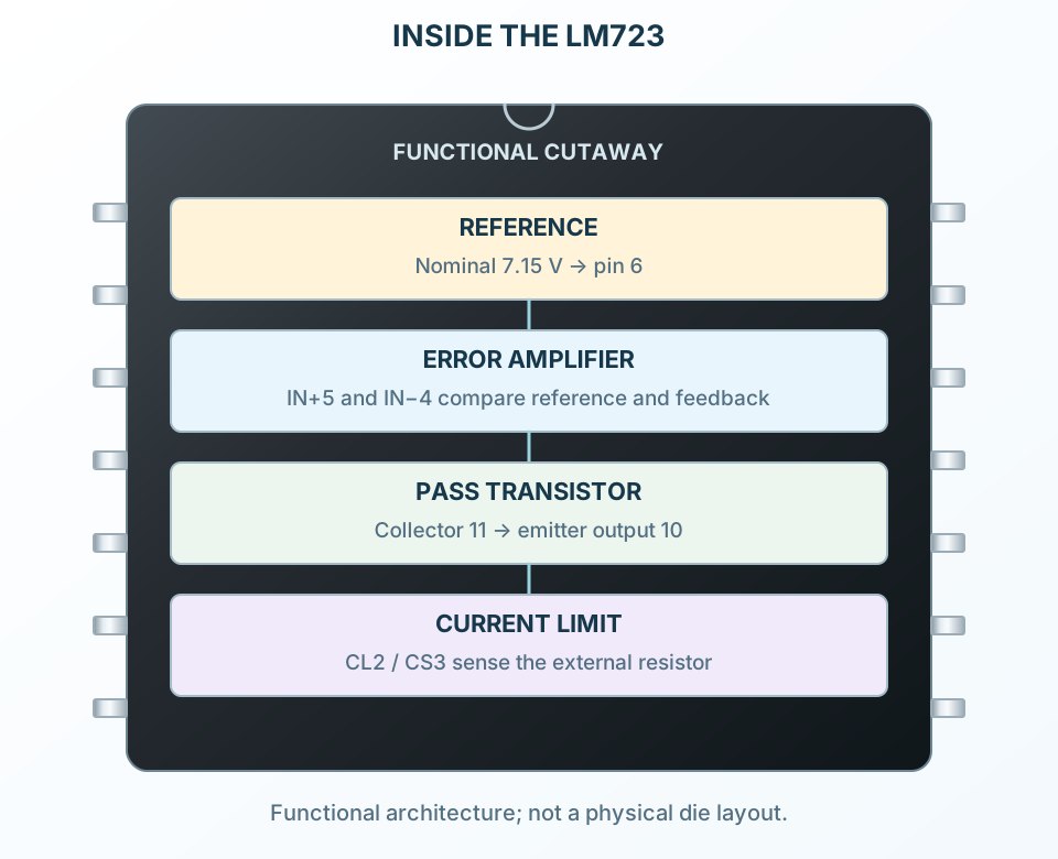
Explore the circuit
Select a stage to see its role and connections
Input
Divide the reference to the intended output level.
Control
Compare that level against the sensed regulated output.
Output
Adjust pass current; the sense resistor activates current limiting.
Selected packagePDIP-14LM723CN
Physical connections14 pinsPackage-specific numbering
Reference collection6 tables38 parameters & pin functions
Pin reference
Signal names, electrical functions and connection guidance
Physical pin numbers14 pins
Scroll within the table to see all columns and rows.
| Pin | Signal | Type | Function & connection |
|---|---|---|---|
| NC | No connection | Unused contactConnection guidanceLeave unconnected. | |
| CL | Input / control | Current-limit transistor baseConnection guidanceConnect to OUT10 before the 10 Ω sense resistor. | |
| CS | Input / control | Current-sense transistor emitterConnection guidanceConnect to the regulated output after the sense resistor. | |
| IN− | Input / control | Error amplifier feedbackConnection guidanceConnect to the regulated output through 3 kΩ; connect compensation capacitor here. | |
| IN+ | Input / control | Error amplifier reference inputConnection guidanceConnect to the 4.3 kΩ / 10 kΩ reference-divider junction. | |
| VREF | Input / control | Nominal 7.15 V referenceConnection guidanceConnect 4.3 kΩ to IN+5; 10 kΩ from IN+5 to ground. | |
| V− | Supply | Control-circuit returnConnection guidanceConnect to ground. | |
| NC | No connection | Unused contactConnection guidanceLeave unconnected. | |
| VZ | Input / control | Internal zener connectionConnection guidanceLeave open in this positive-output example. | |
| OUT | Output | Internal pass emitterConnection guidanceConnect CL2 and the input side of the 10 Ω sense resistor. | |
| VC | Supply | Pass-transistor collectorConnection guidanceConnect to +12 V. | |
| V+ | Supply | Control-circuit positive supplyConnection guidanceConnect to +12 V; bypass locally to ground. | |
| COMP | Input / control | Frequency compensationConnection guidanceConnect 100 pF between COMP13 and IN−4. | |
| NC | No connection | Unused contactConnection guidanceLeave unconnected. |
No pins match these filters. Try another signal name or reset the filters.
Operating reference
ST LM723C selected grade
Manufacturer-referenced values5 parameters
Scroll within the table to see all columns and rows.
| Parameter | Value | Conditions / notes |
|---|---|---|
| Supply range | 9.5–40 V | Maintain input/output headroom |
| Output range | 2–37 V | Appropriate external circuit required |
| Ambient | 0–70°C | LM723C; not extended-grade LM723 |
| Reference | 6.8–7.5 V; 7.15 V typical | IREF = 160 µA |
| Internal output capability | Up to 150 mA | Package dissipation and headroom limit actual use |
No specifications match. Try a parameter name or a unit.
Do not substitute extended-grade limits for the commercial parts.
Regulation and reference
25°C, manufacturer test circuit
Manufacturer-referenced values6 parameters
Scroll within the table to see all columns and rows.
| Parameter | Value | Conditions / notes |
|---|---|---|
| Line regulation | 0.01% typical; 0.1% max | 12–15 V input |
| Wide-range line regulation | 0.1% typical; 0.5% max | 12–40 V input |
| Load regulation | 0.03% typical; 0.2% max | 1–50 mA |
| Quiescent current | 2.3 mA typical; 4 mA max | 30 V input; no load |
| Ripple rejection | 74 dB typical | 100 Hz–10 kHz; no reference bypass |
| Current limit | 65 mA typical | RSC = 10 Ω; output shorted |
No specifications match. Try a parameter name or a unit.
Regulation values exclude changing junction temperature.
Five-volt circuit
Nominal calculation
Manufacturer-referenced values7 parameters
Scroll within the table to see all columns and rows.
| Parameter | Value | Conditions / notes |
|---|---|---|
| Input | 12 V | V+12 and VC11 |
| Reference divider | 4.3 kΩ / 10 kΩ | VREF6 → 4.3k → IN+5 → 10k → GND |
| Nominal output | 7.15 × 10 / 14.3 = 5 V | Reference and resistor tolerances remain |
| Current sense | 10 Ω | OUT10/CL2 → resistor → regulated output/CS3 |
| Feedback | 3 kΩ to IN−4 | From the regulated output |
| Compensation | 100 pF | COMP13 to IN−4 |
| Load | 1 kΩ | About 5 mA and 25 mW |
No specifications match. Try a parameter name or a unit.
No external pass transistor is needed for this small example.
Thermal and stress limits
LM723CN · PDIP-14
Manufacturer-referenced values6 parameters
Scroll within the table to see all columns and rows.
| Parameter | Value | Conditions / notes |
|---|---|---|
| Lead pitch | 2.54 mm | Through-hole |
| Input stress ceiling | 40 V | Do not exceed |
| Reference output stress current | 25 mA | LM723C absolute maximum; avoid designing at it |
| Maximum junction | 125°C | Selected commercial grade |
| θJA reference | 200°C/W DIP; 160°C/W SO14 | Manufacturer reference mounting |
| Storage | −65 to +150°C | Unpowered |
No specifications match. Try a parameter name or a unit.
A headline current limit does not remove the package power limit.
External connections
Physical package contacts
Manufacturer-referenced values14 parameters
Scroll within the table to see all columns and rows.
| Parameter | Value | Conditions / notes |
|---|---|---|
| 1 · NC | Unused contact | Leave unconnected. |
| 2 · CL | Current-limit transistor base | Connect to OUT10 before the 10 Ω sense resistor. |
| 3 · CS | Current-sense transistor emitter | Connect to the regulated output after the sense resistor. |
| 4 · IN− | Error amplifier feedback | Connect to the regulated output through 3 kΩ; connect compensation capacitor here. |
| 5 · IN+ | Error amplifier reference input | Connect to the 4.3 kΩ / 10 kΩ reference-divider junction. |
| 6 · VREF | Nominal 7.15 V reference | Connect 4.3 kΩ to IN+5; 10 kΩ from IN+5 to ground. |
| 7 · V− | Control-circuit return | Connect to ground. |
| 8 · NC | Unused contact | Leave unconnected. |
| 9 · VZ | Internal zener connection | Leave open in this positive-output example. |
| 10 · OUT | Internal pass emitter | Connect CL2 and the input side of the 10 Ω sense resistor. |
| 11 · VC | Pass-transistor collector | Connect to +12 V. |
| 12 · V+ | Control-circuit positive supply | Connect to +12 V; bypass locally to ground. |
| 13 · COMP | Frequency compensation | Connect 100 pF between COMP13 and IN−4. |
| 14 · NC | Unused contact | Leave unconnected. |
No specifications match. Try a parameter name or a unit.
Connect all supply and return contacts; leave only explicitly unused contacts open.
No matching rowsTry a pin name, parameter, unit or test condition, or reset the filters.
Circuit development
Use the reviewed basic circuit as a starting point, then verify load and temperature limits.
Manufacturer application guideEngineering education
Compare the internal functional blocks with the external connections.
Manufacturer application guidePCB integration
Choose the correct package and check the downloaded footprint before manufacture.
Manufacturer application guideTake it into ProTech
Find LM723 in the Components Library to place its schematic symbol and connect its pins.
Reference page · circuit simulation model not yet availableOpen ProTech