Real View
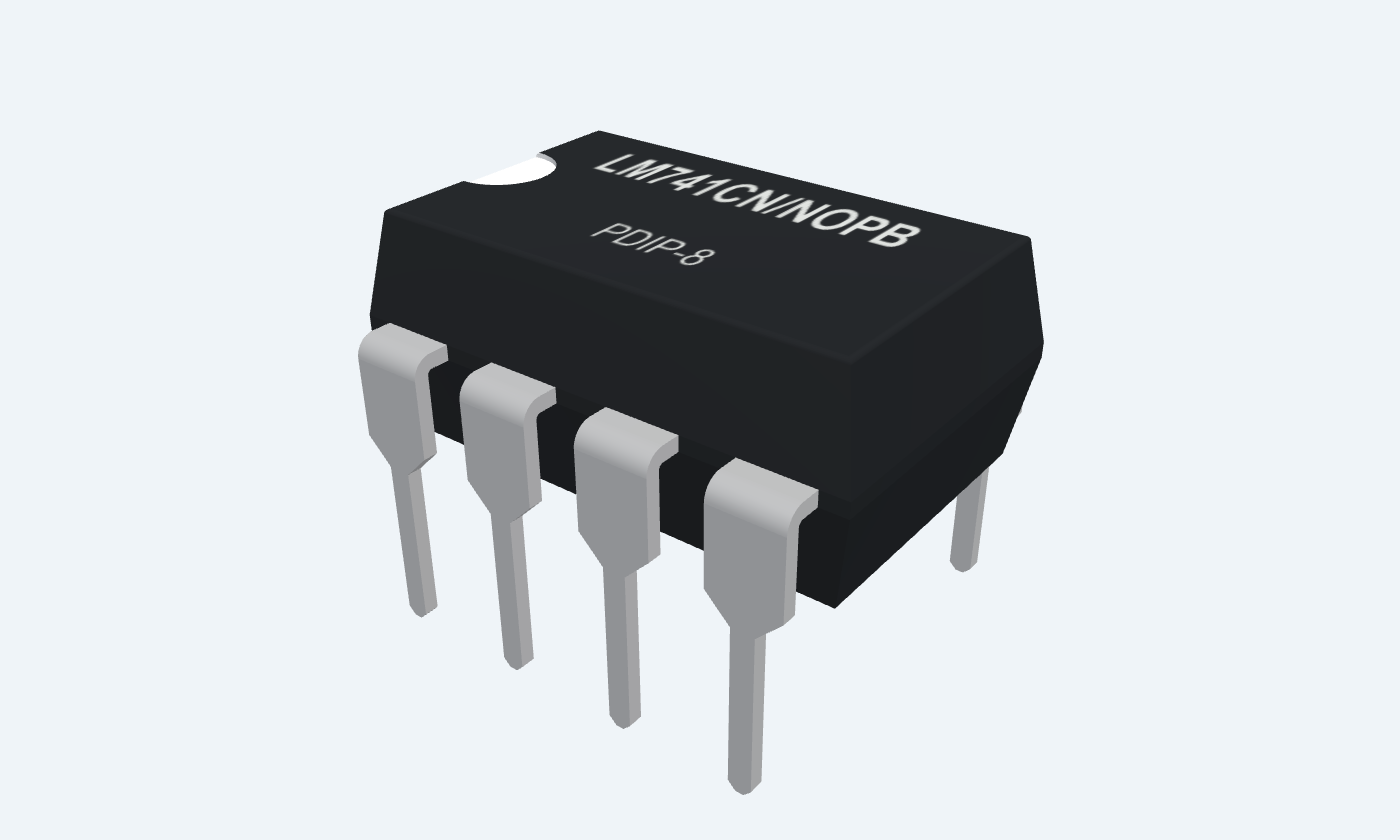
Understand analog gain through negative feedback.
LM741 is a classic single operational amplifier with a bipolar input stage, internal compensation and dedicated offset-adjustment pins. Negative feedback turns its high open-loop gain into a predictable closed-loop circuit. Our example uses a ±15 V supply and a gain of ten: a 0.20 V input ideally becomes 2.00 V. The supply midpoint is the signal ground; it is separate from the IC’s negative power pin. This page uses the commercial LM741CN/NOPB in PDIP-8. The reviewed TI document removed the obsolete SOIC package, so this reference does not offer a fabricated SMD counterpart.
Select a pin to explore its connection
Click a lead or use the arrow keys. Top view
One end of the optional offset-null network.
Leave open in the basic example.
Use the manufacturer trim circuit when offset adjustment is required.
Negative feedback input.
Connect to the 90 kΩ / 10 kΩ feedback junction.
Positive signal input.
Apply the 0.20 V input signal relative to the supply midpoint.
Negative power rail.
Connect to −15 V; bypass locally to the 0 V midpoint.
This is not ground in the illustrated split-supply circuit.
Other end of the optional offset-null network.
Leave open in the basic example.
Amplified output signal.
Connect the 90 kΩ feedback resistor and a high-impedance meter.
Output needs headroom from both supply rails.
Positive power rail.
Connect to +15 V; bypass locally to the 0 V midpoint.
No electrical connection is specified for this contact.
Leave unconnected.
Use the signal midpoint and two supply rails correctly. The output cannot reach either rail.
LM741CN/NOPB · PDIP-8
| Property | Details |
|---|---|
| Manufacturer | Texas Instruments |
| Part number | LM741CN/NOPB |
| Package | PDIP-8 |
| Connections | 8 pins |
| Mounting | Through-hole |
| Lead pitch | 2.54 mm |
| Package code | dip |
| Thermal reference | Board and package dependent; see manufacturer data |
Commercial LM741C reference
Scroll sideways to see all columns.
| Parameter | Value | Conditions / notes |
|---|---|---|
| Recommended split supply | ±10 to ±18 V | TI operating table; ±15 V nominal |
| Ambient temperature | 0 to +70°C | LM741C grade |
| Example rails | +15 V / −15 V | 30 V total span; midpoint is 0 V |
| Input common-mode range | ±12 V minimum; ±13 V typical | ±15 V supply; 25°C |
| Local bypass | 100 nF from each rail to midpoint | Short paths near pins 7 and 4 |
No specifications match. Try a parameter name or a unit.
Do not substitute military-grade limits or assume modern rail-to-rail operation.
LM741C · ±15 V · 25°C unless stated
Scroll sideways to see all columns.
| Parameter | Value | Conditions / notes |
|---|---|---|
| Input offset | 2 mV typical; 6 mV maximum | RS ≤ 10 kΩ |
| Input bias current | 80 nA typical; 500 nA maximum | Magnitude; specified test conditions |
| Input offset current | 20 nA typical; 200 nA maximum | Difference between the input currents |
| Supply current | 1.7 mA typical; 2.8 mA maximum | No external output load |
| Open-loop gain | 200 V/mV typical; 20 minimum | VO = ±10 V; RL ≥ 2 kΩ |
No specifications match. Try a parameter name or a unit.
Input offset is multiplied by the closed-loop noise gain. Bias-current errors depend on the source resistances.
Specified test conditions
Scroll sideways to see all columns.
| Parameter | Value | Conditions / notes |
|---|---|---|
| Output swing, RL ≥ 10 kΩ | ±14 V typical; ±12 V minimum | ±15 V supply |
| Output swing, RL ≥ 2 kΩ | ±13 V typical; ±10 V minimum | ±15 V supply |
| Slew rate | 0.5 V/µs typical | 25°C; unity gain |
| Small-signal rise time | 0.3 µs typical | 25°C; unity gain |
| Large sine-wave requirement | SR ≥ 2π f VPEAK | Engineering design relation, not a new device rating |
No specifications match. Try a parameter name or a unit.
Load, amplitude and frequency matter together. A slow DC example does not establish high-frequency performance.
Non-inverting connection
Scroll sideways to see all columns.
| Parameter | Value | Conditions / notes |
|---|---|---|
| VIN | 0.20 V | Pin 3, referenced to 0 V |
| Rf | 90 kΩ | Pin 6 to pin 2 |
| Rg | 10 kΩ | Pin 2 to 0 V |
| Nominal gain | 10 V/V | 1 + Rf / Rg |
| Ideal output | 2.00 V | 0.20 V × 10 |
| Feedback node | 0.20 V nominal | Output divided by ten |
| Null pins / NC | 1, 5 and 8 left open | Optional trim is not used |
No specifications match. Try a parameter name or a unit.
An illustrative light-load DC example; it is not a precision or rail-to-rail claim.
LM741CN/NOPB · PDIP-8
Scroll sideways to see all columns.
| Parameter | Value | Conditions / notes |
|---|---|---|
| Lead pitch | 2.54 mm | Through-hole |
| Inputs | IN− 2; IN+ 3 | Differential signal pair |
| Output | 6 | Amplifier output |
| Power | V− 4; V+ 7 | Both rails are required for this circuit |
| Offset adjustment | 1 and 5 | See manufacturer trim circuit |
| No connection | 8 | Leave open |
No specifications match. Try a parameter name or a unit.
PDIP top view; orient the notch before counting pins.
Select a pin for its function, connection guidance and electrical notes.
Follow the labeled connections and functional stages
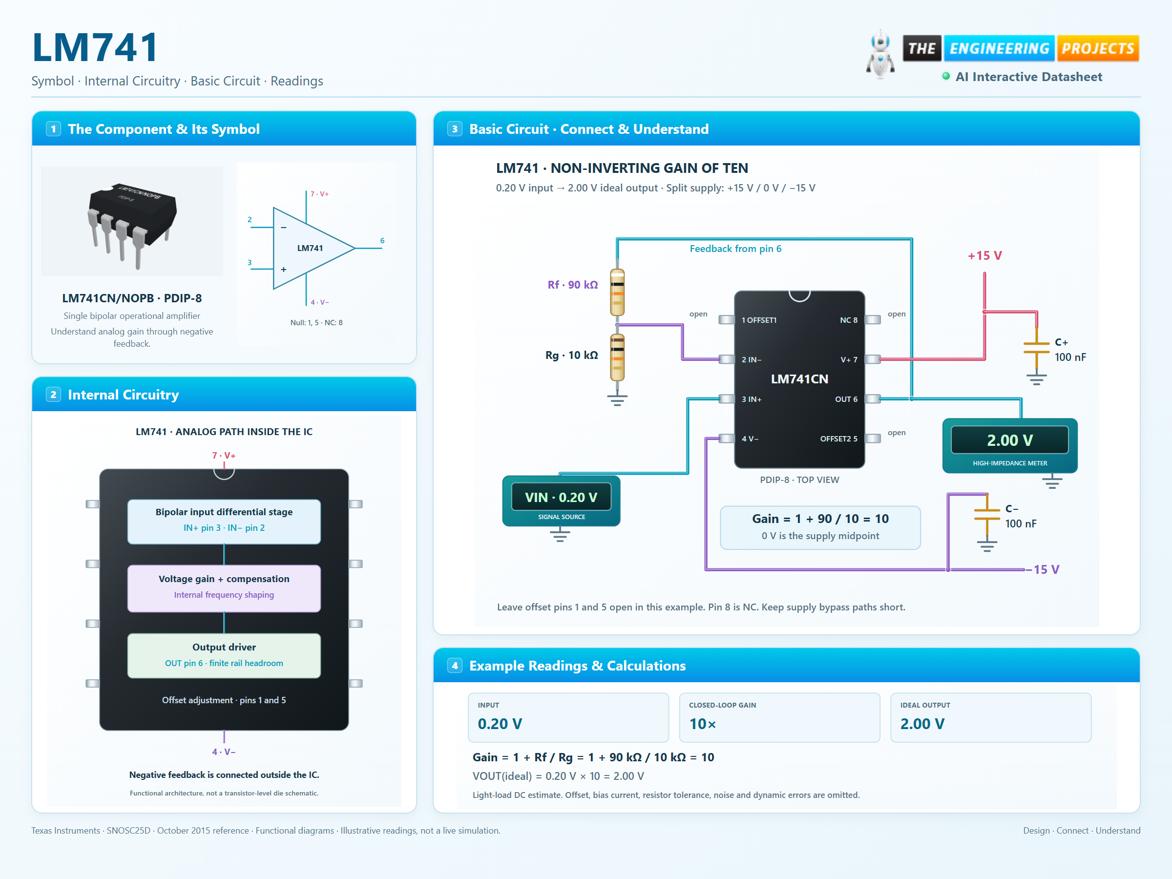
3 stages · Explore one step at a time
The input stage responds to the difference between pins 3 and 2. Small input errors can cause large output changes without feedback.
The 90 kΩ and 10 kΩ network returns one tenth of the output to IN−. Negative feedback brings this near the voltage at IN+.
With ±15 V rails, the example has comfortable headroom. Input offset and bias currents introduce DC error; bandwidth, slew rate and loading limit changing signals.
A physical eight-pin IC and a clearly routed feedback loop.
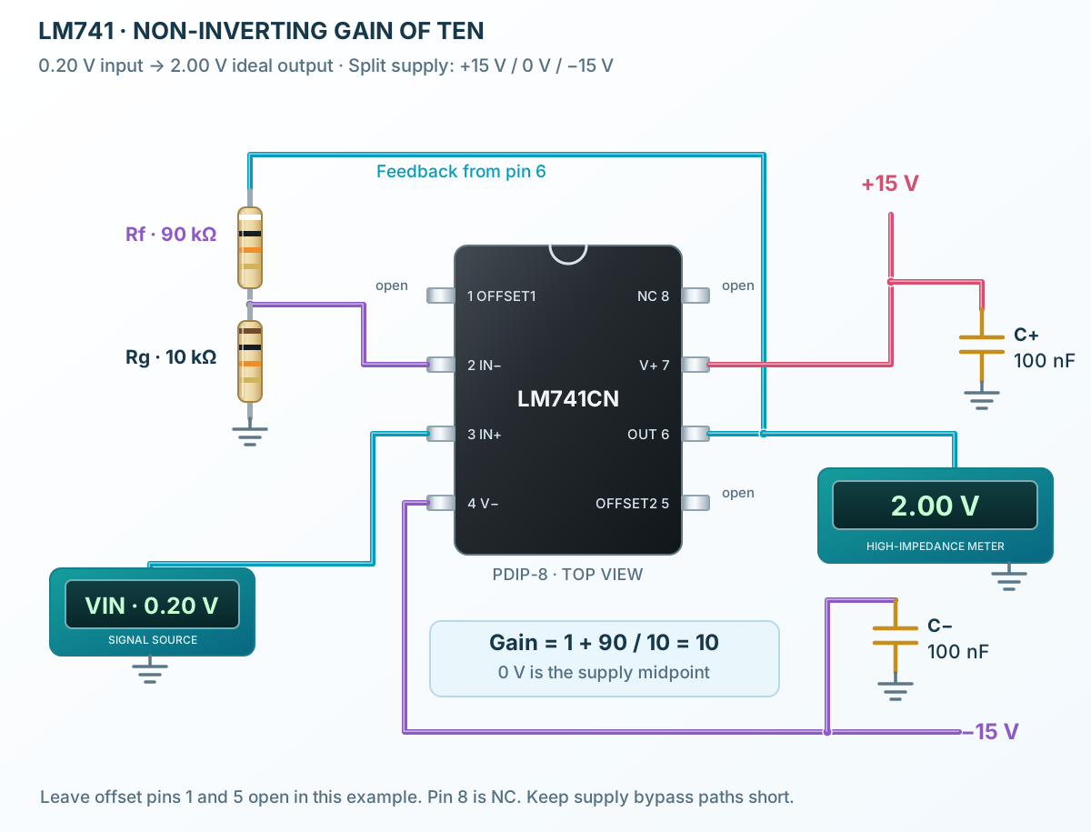
Follow the component values and pin connections
Pin 7 uses +15 V and pin 4 uses −15 V. Bypass both rails to their common midpoint.
90 kΩ connects OUT to IN−, and 10 kΩ connects IN− to the midpoint.
Apply 0.20 V to IN+. A high-impedance meter reads approximately 2.00 V before device errors.
Input, gain, compensation and output stages inside one IC.
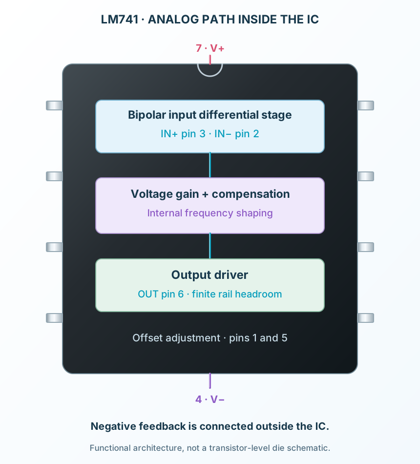
Select a stage to see its role and connections
The input pair senses a small voltage difference and draws finite input bias current.
Internal voltage gain is frequency-compensated to support ordinary feedback configurations.
The output stage supplies the load within its voltage, current and thermal limits.
Signal names, electrical functions and connection guidance
Scroll within the table to see all columns and rows.
| Pin | Signal | Type | Function & connection |
|---|---|---|---|
| OFFSET1 | Offset adjustment | One end of the optional offset-null network.Connection guidanceLeave open in the basic example. Use the manufacturer trim circuit when offset adjustment is required. | |
| IN− | Inverting input | Negative feedback input.Connection guidanceConnect to the 90 kΩ / 10 kΩ feedback junction. | |
| IN+ | Non-inverting input | Positive signal input.Connection guidanceApply the 0.20 V input signal relative to the supply midpoint. | |
| V− | Negative supply | Negative power rail.Connection guidanceConnect to −15 V; bypass locally to the 0 V midpoint. This is not ground in the illustrated split-supply circuit. | |
| OFFSET2 | Offset adjustment | Other end of the optional offset-null network.Connection guidanceLeave open in the basic example. | |
| OUT | Analog output | Amplified output signal.Connection guidanceConnect the 90 kΩ feedback resistor and a high-impedance meter. Output needs headroom from both supply rails. | |
| V+ | Positive supply | Positive power rail.Connection guidanceConnect to +15 V; bypass locally to the 0 V midpoint. | |
| NC | No connection | No electrical connection is specified for this contact.Connection guidanceLeave unconnected. |
No pins match these filters. Try another signal name or reset the filters.
Commercial LM741C reference
Scroll within the table to see all columns and rows.
| Parameter | Value | Conditions / notes |
|---|---|---|
| Recommended split supply | ±10 to ±18 V | TI operating table; ±15 V nominal |
| Ambient temperature | 0 to +70°C | LM741C grade |
| Example rails | +15 V / −15 V | 30 V total span; midpoint is 0 V |
| Input common-mode range | ±12 V minimum; ±13 V typical | ±15 V supply; 25°C |
| Local bypass | 100 nF from each rail to midpoint | Short paths near pins 7 and 4 |
No specifications match. Try a parameter name or a unit.
Do not substitute military-grade limits or assume modern rail-to-rail operation.
LM741C · ±15 V · 25°C unless stated
Scroll within the table to see all columns and rows.
| Parameter | Value | Conditions / notes |
|---|---|---|
| Input offset | 2 mV typical; 6 mV maximum | RS ≤ 10 kΩ |
| Input bias current | 80 nA typical; 500 nA maximum | Magnitude; specified test conditions |
| Input offset current | 20 nA typical; 200 nA maximum | Difference between the input currents |
| Supply current | 1.7 mA typical; 2.8 mA maximum | No external output load |
| Open-loop gain | 200 V/mV typical; 20 minimum | VO = ±10 V; RL ≥ 2 kΩ |
No specifications match. Try a parameter name or a unit.
Input offset is multiplied by the closed-loop noise gain. Bias-current errors depend on the source resistances.
Specified test conditions
Scroll within the table to see all columns and rows.
| Parameter | Value | Conditions / notes |
|---|---|---|
| Output swing, RL ≥ 10 kΩ | ±14 V typical; ±12 V minimum | ±15 V supply |
| Output swing, RL ≥ 2 kΩ | ±13 V typical; ±10 V minimum | ±15 V supply |
| Slew rate | 0.5 V/µs typical | 25°C; unity gain |
| Small-signal rise time | 0.3 µs typical | 25°C; unity gain |
| Large sine-wave requirement | SR ≥ 2π f VPEAK | Engineering design relation, not a new device rating |
No specifications match. Try a parameter name or a unit.
Load, amplitude and frequency matter together. A slow DC example does not establish high-frequency performance.
Non-inverting connection
Scroll within the table to see all columns and rows.
| Parameter | Value | Conditions / notes |
|---|---|---|
| VIN | 0.20 V | Pin 3, referenced to 0 V |
| Rf | 90 kΩ | Pin 6 to pin 2 |
| Rg | 10 kΩ | Pin 2 to 0 V |
| Nominal gain | 10 V/V | 1 + Rf / Rg |
| Ideal output | 2.00 V | 0.20 V × 10 |
| Feedback node | 0.20 V nominal | Output divided by ten |
| Null pins / NC | 1, 5 and 8 left open | Optional trim is not used |
No specifications match. Try a parameter name or a unit.
An illustrative light-load DC example; it is not a precision or rail-to-rail claim.
LM741CN/NOPB · PDIP-8
Scroll within the table to see all columns and rows.
| Parameter | Value | Conditions / notes |
|---|---|---|
| Lead pitch | 2.54 mm | Through-hole |
| Inputs | IN− 2; IN+ 3 | Differential signal pair |
| Output | 6 | Amplifier output |
| Power | V− 4; V+ 7 | Both rails are required for this circuit |
| Offset adjustment | 1 and 5 | See manufacturer trim circuit |
| No connection | 8 | Leave open |
No specifications match. Try a parameter name or a unit.
PDIP top view; orient the notch before counting pins.
No matching rowsTry a pin name, parameter, unit or test condition, or reset the filters.
Demonstrate feedback and gain using low-frequency signals and suitable supply rails.
Manufacturer application guideCombine inputs through an inverting summing network; account for bias-current and offset errors.
Manufacturer application guideUse capacitors in feedback networks with a defined DC path and suitable frequency range.
Manufacturer application guideFind LM741 in the Components Library to place its schematic symbol and connect its pins.
Reference page · circuit simulation model not yet availableOpen ProTech