LMV358MLow-voltage dual operational amplifier
Amplify small signals close to the output rails.
LMV358M contains two low-voltage operational amplifiers in one eight-pin surface-mount package. Negative feedback makes their output voltages follow a controlled multiple of the input signal. This page follows the TI LMV358-N family and the LMV358M/NOPB SOIC orderable part, reusing its existing component identity. The device operates from 2.7–5.5 V and has a rail-to-rail output stage. That description does not apply to its inputs: at a 5 V supply, the specified common-mode range is 0–4 V. Loading, temperature and output current determine how closely the output reaches either rail. The example runs from 5 V with Rf = 20 kΩ and Rg = 10 kΩ. An input of 0.50 V requests an ideal 1.50 V output. The unused channel is connected as a follower so neither input floats. The selected SOIC package, pin map and downloadable footprint stay consistent across all views.
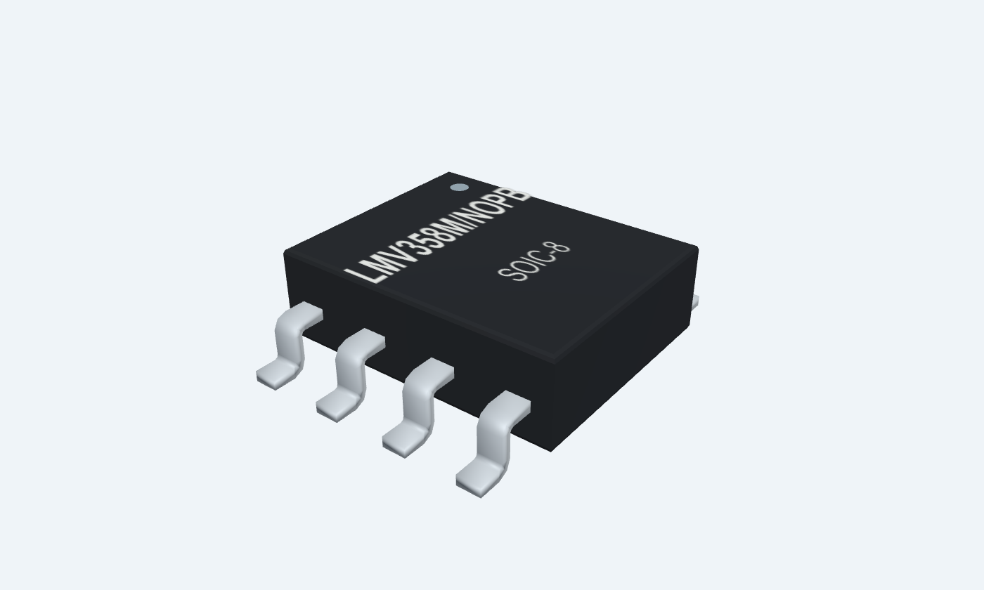

8Physical pins
LMV358M/NOPBSOIC-8
Manufacturer-referencedTexas Instruments
Pin diagram
Select a pin to explore its connection
Highlight
LMV358MSOIC-8Top view
Click a lead or use the arrow keys. Top view
PIN 1 · Analog outputs
Analog outputOUT A
Function
Output of amplifier A.
How to connect
Connect Rf to IN A− and measure this node.
Electrical note
Output swing depends on load and temperature.
PIN 2 · Signal and feedback inputs
Inverting inputIN A−
Function
Feedback input of amplifier A.
How to connect
Connect the Rf/Rg junction.
PIN 3 · Signal and feedback inputs
Non-inverting inputIN A+
Function
Signal input of amplifier A.
How to connect
Apply VIN relative to ground.
Electrical note
Input common-mode range is not rail-to-rail.
PIN 4 · Supply
Negative supplyV−
Function
Shared lower supply rail.
How to connect
Connect to ground for the shown 5 V circuit.
PIN 5 · Signal and feedback inputs
Non-inverting inputIN B+
Function
Signal input of amplifier B.
How to connect
Connect to VIN in this example.
PIN 6 · Signal and feedback inputs
Inverting inputIN B−
Function
Feedback input of amplifier B.
How to connect
Join OUT B for a voltage follower.
PIN 7 · Analog outputs
Analog outputOUT B
Function
Independent amplifier B output.
How to connect
Join IN B− and leave otherwise unloaded.
PIN 8 · Supply
Positive supplyV+
Function
Shared positive rail.
How to connect
Apply 5 V and bypass to pin 4 with 100 nF.
Electrical note
Recommended supply 2.7–5.5 V; unlike LM358, this is not a high-voltage amplifier.
Key specifications
Amplify small signals close to the output rails.
Recommended supply2.7–5.5 V
Gain-bandwidth1 MHz typical
Operating ambient−40–125 °C
Both amplifiers210 µA typical at 5 V
Package details
LMV358M/NOPB · SOIC-8
| Property | Details |
|---|---|
| Manufacturer | Texas Instruments |
| Part number | LMV358M/NOPB |
| Package | SOIC-8 |
| Connections | 8 pins |
| Mounting | SMD |
| Lead pitch | 1.27 mm |
| Package code | SOIC-8 |
| Thermal reference | See operating and package limits |
Operating conditions
LMV358-N · LMV358M/NOPB
Manufacturer specifications 5 parameters
Scroll sideways to see all columns.
| Parameter | Value | Conditions / notes |
|---|---|---|
| Supply | 2.7–5.5 V | Recommended range |
| Ambient temperature | −40 to +125°C | Selected industrial part |
| Input common-mode range at 5 V | 0–4 V specified; −0.2–4.2 V typical | CMRR ≥ 50 dB |
| Supply current, both channels | 210 µA typical; 440 µA max | 5 V, 25°C; 615 µA max over temperature |
| Supply absolute maximum | 5.5 V | Stress limit; do not exceed |
No specifications match. Try a parameter name or a unit.
Typical extensions are not guaranteed operating margins.
Input accuracy
5 V and 25°C unless stated
Manufacturer specifications 5 parameters
Scroll sideways to see all columns.
| Parameter | Value | Conditions / notes |
|---|---|---|
| Input offset | 1.7 mV typical; 7 mV max | 9 mV max over temperature |
| Offset drift | 5 µV/°C typical | Not a guaranteed maximum |
| Input bias | 15 nA typical; 250 nA max | 500 nA max over temperature |
| Input offset current | 5 nA typical; 50 nA max | 150 nA max over temperature |
| Common-mode rejection | 65 dB typical; 50 dB min | 0–4 V common-mode input |
No specifications match. Try a parameter name or a unit.
Bias current through high source resistance adds an input error.
Speed and output
Conditions matter
Manufacturer specifications 6 parameters
Scroll sideways to see all columns.
| Parameter | Value | Conditions / notes |
|---|---|---|
| Gain-bandwidth | 1 MHz typical | 200 pF load |
| Slew rate | 1 V/µs typical | Manufacturer AC test |
| HIGH output, 2 kΩ to midpoint | V+−40 mV typical; V+−300 mV min | 5 V, 25°C |
| LOW output, 2 kΩ to midpoint | 120 mV typical; 300 mV max | 5 V, 25°C |
| Over-temperature swing, 2 kΩ | Within 400 mV of either rail | Specified test load |
| Short-circuit current | 40 mA typical | Not a recommended continuous load current |
No specifications match. Try a parameter name or a unit.
Rail-to-rail does not mean zero headroom at every current.
Gain-three example
5 V supply; light load
Manufacturer specifications 6 parameters
Scroll sideways to see all columns.
| Parameter | Value | Conditions / notes |
|---|---|---|
| Input / ideal output | 0.50 V / 1.50 V | After settling, while linear |
| Feedback resistor Rf | 20 kΩ | OUT A1 to IN A−2 |
| Ground resistor Rg | 10 kΩ | IN A−2 to GND |
| Signal | VIN to pins 3 and 5 | Common ground |
| Second channel | Join pins 6 and 7 | Voltage follower; output otherwise unloaded |
| Bypass | 100 nF | Pins 8 to 4, close to the IC |
No specifications match. Try a parameter name or a unit.
Use a high-impedance meter. The explorer uses conservative fixed headroom, not a transistor-level simulation.
Package and limits
LMV358M/NOPB · SOIC-8
Manufacturer specifications 5 parameters
Scroll sideways to see all columns.
| Parameter | Value | Conditions / notes |
|---|---|---|
| Physical pins | 8 | SOIC top view |
| Pitch | 1.27 mm | SMD |
| Maximum junction | 150°C | Apply thermal derating |
| Storage | −65 to +150°C | Unpowered |
| Other package | LMV358MM/NOPB uses VSSOP8 | Different footprint; not interchangeable with SOIC |
No specifications match. Try a parameter name or a unit.
No through-hole part is invented for this surface-mount device.
Connections by function
Select a pin for its function, connection guidance and electrical notes.
Analog outputs2 pins
Signal and feedback inputs4 pins
Supply2 pins
LMV358M at a glance
Follow the labeled connections and functional stages
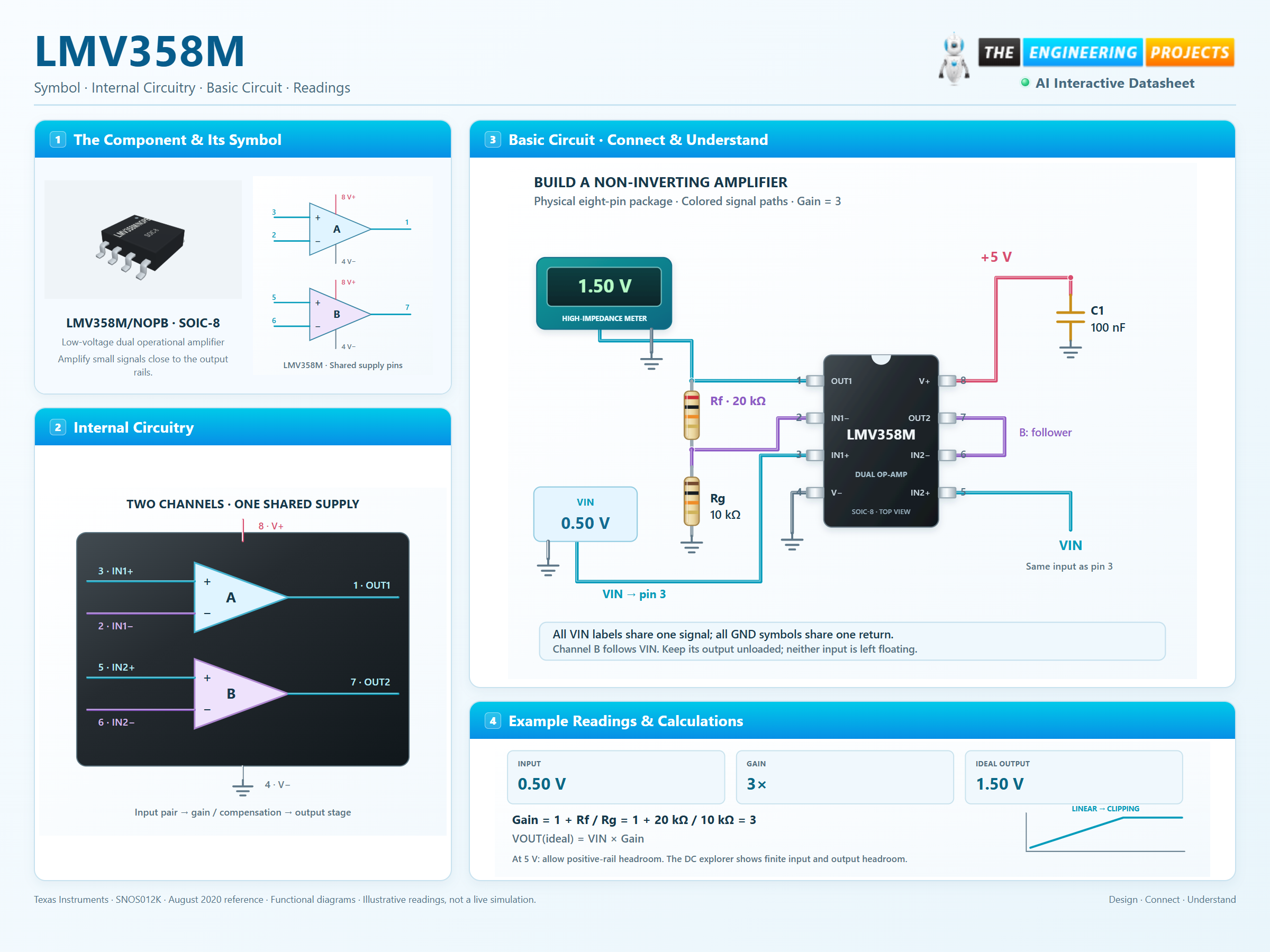
How it works
3 stages · Explore one step at a time
Compare
Each amplifier senses the difference between its two inputs.
Feed back
The resistor network returns a fraction of the output to the inverting input.
Stay within limits
The output settles near VIN × (1 + Rf/Rg) until input range or output headroom is exceeded.
Step 1 of 3
LMV358M in a circuit
SOIC8 with clear signal, feedback and supply paths.
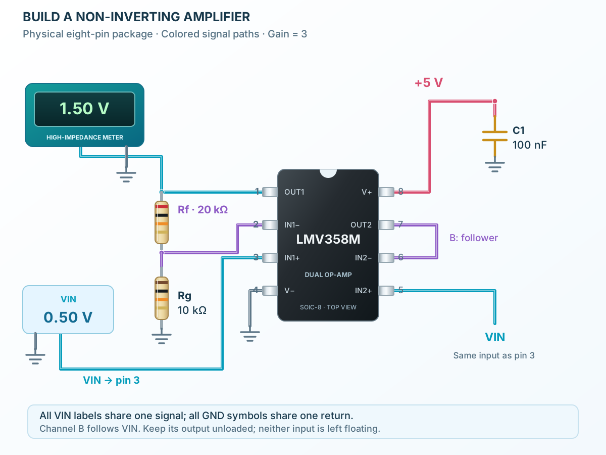
Connect it, step by step
Follow the component values and pin connections
Power
Connect 5 V to pin 8 and ground to pin 4; add local bypass.
Feedback
Connect the 20 kΩ and 10 kΩ network to channel A.
Measure
A settled 0.50 V input gives an ideal 1.50 V output while linear.
Try the amplifier
Change the input and feedback. See the gain and output respond.
Closed-loop gain—
Ideal output—
Estimated output—
Enable JavaScript to explore the amplifier.
Estimated outputIdeal gainInput outside recommended range
Gain = 1 + Rf / Rg · VOUT(ideal) = VIN × Gain
Illustrative DC envelope: 0.4–4.6 V output and 0–4 V input at a 5 V supply. Real limits depend on load and temperature; offset, noise and dynamic response are omitted.
Inside LMV358M
Independent channels share supply and bias.
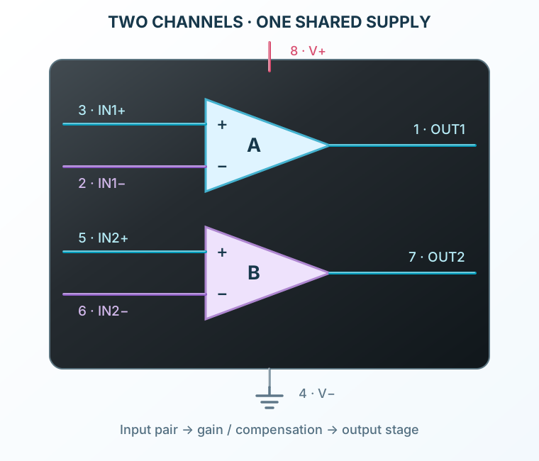
Explore the circuit
Select a stage to see its role and connections
Input
Bipolar inputs sense differential voltage.
Gain
Internal gain and compensation support stable feedback operation.
Output
Output stages drive the load close to the rails under the stated conditions.
Selected packageSOIC-8LMV358M/NOPB
Physical connections8 pinsPackage-specific numbering
Reference collection6 tables27 parameters & pin functions
Pin reference
Signal names, electrical functions and connection guidance
Physical pin numbers8 pins
Scroll within the table to see all columns and rows.
| Pin | Signal | Type | Function & connection |
|---|---|---|---|
| OUT A | Analog output | Output of amplifier A.Connection guidanceConnect Rf to IN A− and measure this node. Output swing depends on load and temperature. | |
| IN A− | Inverting input | Feedback input of amplifier A.Connection guidanceConnect the Rf/Rg junction. | |
| IN A+ | Non-inverting input | Signal input of amplifier A.Connection guidanceApply VIN relative to ground. Input common-mode range is not rail-to-rail. | |
| V− | Negative supply | Shared lower supply rail.Connection guidanceConnect to ground for the shown 5 V circuit. | |
| IN B+ | Non-inverting input | Signal input of amplifier B.Connection guidanceConnect to VIN in this example. | |
| IN B− | Inverting input | Feedback input of amplifier B.Connection guidanceJoin OUT B for a voltage follower. | |
| OUT B | Analog output | Independent amplifier B output.Connection guidanceJoin IN B− and leave otherwise unloaded. | |
| V+ | Positive supply | Shared positive rail.Connection guidanceApply 5 V and bypass to pin 4 with 100 nF. Recommended supply 2.7–5.5 V; unlike LM358, this is not a high-voltage amplifier. |
No pins match these filters. Try another signal name or reset the filters.
Operating conditions
LMV358-N · LMV358M/NOPB
Manufacturer-referenced values5 parameters
Scroll within the table to see all columns and rows.
| Parameter | Value | Conditions / notes |
|---|---|---|
| Supply | 2.7–5.5 V | Recommended range |
| Ambient temperature | −40 to +125°C | Selected industrial part |
| Input common-mode range at 5 V | 0–4 V specified; −0.2–4.2 V typical | CMRR ≥ 50 dB |
| Supply current, both channels | 210 µA typical; 440 µA max | 5 V, 25°C; 615 µA max over temperature |
| Supply absolute maximum | 5.5 V | Stress limit; do not exceed |
No specifications match. Try a parameter name or a unit.
Typical extensions are not guaranteed operating margins.
Input accuracy
5 V and 25°C unless stated
Manufacturer-referenced values5 parameters
Scroll within the table to see all columns and rows.
| Parameter | Value | Conditions / notes |
|---|---|---|
| Input offset | 1.7 mV typical; 7 mV max | 9 mV max over temperature |
| Offset drift | 5 µV/°C typical | Not a guaranteed maximum |
| Input bias | 15 nA typical; 250 nA max | 500 nA max over temperature |
| Input offset current | 5 nA typical; 50 nA max | 150 nA max over temperature |
| Common-mode rejection | 65 dB typical; 50 dB min | 0–4 V common-mode input |
No specifications match. Try a parameter name or a unit.
Bias current through high source resistance adds an input error.
Speed and output
Conditions matter
Manufacturer-referenced values6 parameters
Scroll within the table to see all columns and rows.
| Parameter | Value | Conditions / notes |
|---|---|---|
| Gain-bandwidth | 1 MHz typical | 200 pF load |
| Slew rate | 1 V/µs typical | Manufacturer AC test |
| HIGH output, 2 kΩ to midpoint | V+−40 mV typical; V+−300 mV min | 5 V, 25°C |
| LOW output, 2 kΩ to midpoint | 120 mV typical; 300 mV max | 5 V, 25°C |
| Over-temperature swing, 2 kΩ | Within 400 mV of either rail | Specified test load |
| Short-circuit current | 40 mA typical | Not a recommended continuous load current |
No specifications match. Try a parameter name or a unit.
Rail-to-rail does not mean zero headroom at every current.
Gain-three example
5 V supply; light load
Manufacturer-referenced values6 parameters
Scroll within the table to see all columns and rows.
| Parameter | Value | Conditions / notes |
|---|---|---|
| Input / ideal output | 0.50 V / 1.50 V | After settling, while linear |
| Feedback resistor Rf | 20 kΩ | OUT A1 to IN A−2 |
| Ground resistor Rg | 10 kΩ | IN A−2 to GND |
| Signal | VIN to pins 3 and 5 | Common ground |
| Second channel | Join pins 6 and 7 | Voltage follower; output otherwise unloaded |
| Bypass | 100 nF | Pins 8 to 4, close to the IC |
No specifications match. Try a parameter name or a unit.
Use a high-impedance meter. The explorer uses conservative fixed headroom, not a transistor-level simulation.
Package and limits
LMV358M/NOPB · SOIC-8
Manufacturer-referenced values5 parameters
Scroll within the table to see all columns and rows.
| Parameter | Value | Conditions / notes |
|---|---|---|
| Physical pins | 8 | SOIC top view |
| Pitch | 1.27 mm | SMD |
| Maximum junction | 150°C | Apply thermal derating |
| Storage | −65 to +150°C | Unpowered |
| Other package | LMV358MM/NOPB uses VSSOP8 | Different footprint; not interchangeable with SOIC |
No specifications match. Try a parameter name or a unit.
No through-hole part is invented for this surface-mount device.
No matching rowsTry a pin name, parameter, unit or test condition, or reset the filters.
Sensor conditioning
Amplify a slow sensor signal within the input and output limits.
Manufacturer application guideVoltage followers
Buffer a source for a high-impedance load.
Manufacturer application guideActive filters
Combine feedback and RC networks while checking gain-bandwidth and settling.
Manufacturer application guideTake it into ProTech
Find LMV358M in the Components Library to place its schematic symbol and connect its pins.
Reference page · circuit simulation model not yet availableOpen ProTech