Real View
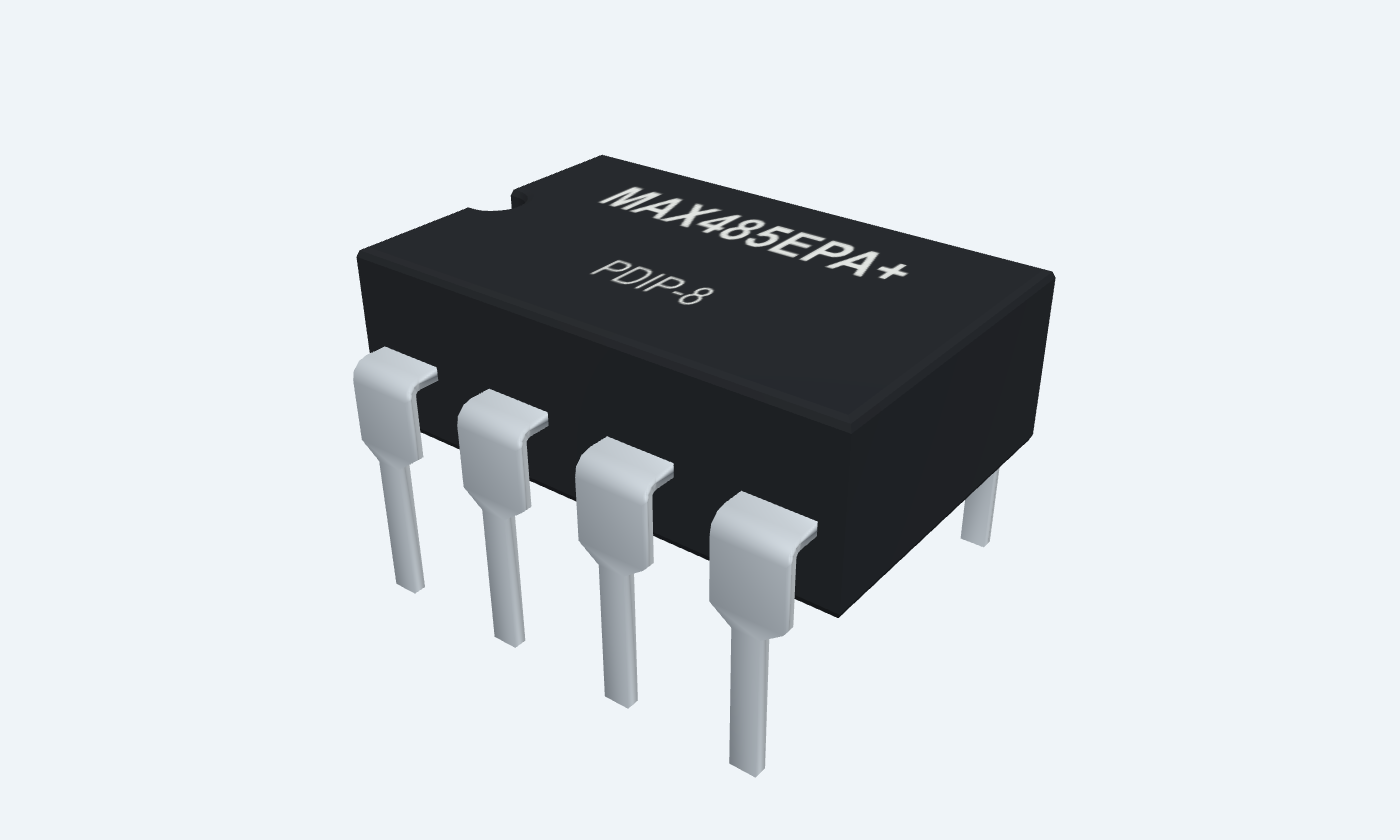
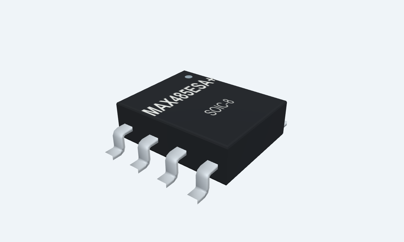
Carry a logic signal across a balanced two-wire bus.
MAX485 connects a controller’s logic-level data to an RS-485 differential bus. One driver and one receiver share terminals A and B, so the link is half duplex: only one node should drive the pair at a time. It does not generate UART framing or implement a protocol by itself. The transceiver runs from a regulated 5 V supply and supports data rates up to 2.5 Mbit/s. DE enables transmission; the active-LOW receiver enable controls RO. Joining those controls provides one direction signal, LOW to receive and HIGH to transmit. The example shows two nodes, termination at both cable ends and one external idle-bias network. A reference conductor keeps the bus common-mode voltage within its operating range. This MAX485 reference does not inherit the shutdown or quarter-unit-load features of other parts in the manufacturer’s family datasheet.
Select a pin to explore its connection
Click a lead or use the arrow keys. Top view
When enabled, HIGH for A − B ≥ 200 mV and LOW for A − B ≤ −200 mV. High impedance when RE̅ is HIGH.
Connect to a 5 V-compatible controller RX input.
Open receiver inputs produce HIGH; a terminated idle bus needs separately designed bias.
LOW enables RO; HIGH releases RO to high impedance.
Join DE for one direction signal: LOW receive, HIGH transmit.
HIGH enables differential driver outputs; LOW releases the bus.
Drive from the direction GPIO; add a 10 kΩ pull-down for a receive-first startup.
With DE HIGH, DI HIGH makes A higher than B. DI LOW reverses the polarity.
Connect to controller UART TX.
Logic HIGH ≥ 2.0 V; LOW ≤ 0.8 V.
Reference for logic levels and bus common-mode voltage.
Join the controller ground and the intended bus reference conductor.
Non-inverting driver output and receiver input.
Connect A to A on the other node using a twisted pair.
Receiver common-mode operating range −7 to +12 V.
Inverting driver output and receiver input.
Connect B to B on the other node; verify vendor naming at third-party terminals.
Powers the transceiver from a nominal 5 V rail.
Use 4.75–5.25 V and 100 nF directly to pin 5.
This is the 5 V MAX485, not a 3.3 V MAX3485.
A differential driver converts DI into opposite bus voltages. A receiver compares A with B and recovers a logic level. Separate enable controls determine who is driving and listening.
MAX485EPA+ · PDIP-8
| Property | Details |
|---|---|
| Manufacturer | Analog Devices / Maxim |
| Part number | MAX485EPA+ |
| Package | PDIP-8 |
| Connections | 8 pins |
| Mounting | Through-hole |
| Lead pitch | 2.54 mm |
| Package code | dip |
| Thermal reference | Board and package dependent; see manufacturer data |
Controls are independent
Scroll sideways to see all columns.
| Parameter | Value | Conditions / notes |
|---|---|---|
| DE HIGH; DI HIGH | A HIGH relative to B | Transmitter enabled |
| DE HIGH; DI LOW | A LOW relative to B | Transmitter enabled |
| DE LOW | A and B driver outputs high impedance | Receiver may remain enabled |
| RE̅ LOW; A − B ≥ +200 mV | RO HIGH | Within common-mode range |
| RE̅ LOW; A − B ≤ −200 mV | RO LOW | Within common-mode range |
| RE̅ HIGH | RO high impedance | External input may need a defined idle state |
| RE̅ LOW; both bus inputs open | RO HIGH | Specified open-input fail-safe |
| DE LOW; RE̅ HIGH | Driver and receiver disabled | MAX485 has no low-current shutdown mode |
No specifications match. Try a parameter name or a unit.
Do not assume a terminated, unbiased idle bus has the same fail-safe behavior as physically open receiver inputs.
Selected industrial grades
Scroll sideways to see all columns.
| Parameter | Value | Conditions / notes |
|---|---|---|
| Supply voltage | 4.75–5.25 V | Nominal 5 V |
| Ambient range | −40 to +85°C | EPA / ESA orderables |
| Logic input HIGH / LOW | ≥ 2.0 V / ≤ 0.8 V | DI, DE and RE̅ |
| RO HIGH / LOW | ≥ 3.5 V / ≤ 0.4 V | Source / sink 4 mA |
| Receiver common-mode | −7 to +12 V | Referenced to local GND |
| Receiver threshold region | −200 to +200 mV | No guaranteed level inside the transition region |
| Typical input hysteresis | 70 mV | Common-mode 0 V |
| Receiver input resistance | 12 kΩ minimum | One standard unit load |
No specifications match. Try a parameter name or a unit.
A 3.3 V controller may drive the logic inputs, but its RX input must tolerate or translate the 5 V RO level.
Manufacturer specified test loads
Scroll sideways to see all columns.
| Parameter | Value | Conditions / notes |
|---|---|---|
| Loaded differential output | 1.5 V minimum | RS-485 test load: two 27 Ω branches |
| No-load current, DE LOW | 300 µA typical; 500 µA maximum | MAX485; defined input levels |
| No-load current, DE HIGH | 500 µA typical; 900 µA maximum | MAX485; driver enabled and unloaded |
| Receiver bus loading | Up to 32 standard unit loads | Bias, cable and other loads also matter |
| Driver protection | Current limiting and thermal shutdown | Not permission for continuous bus contention |
| Slew-rate limiting | Not provided | Use controlled cable topology |
| Low-power shutdown | Not provided in MAX485 | MAX481 / 483 / 487 have different features |
No specifications match. Try a parameter name or a unit.
The MAX487 and MAX1487 quarter-unit-load and 128-node figures do not apply to MAX485.
5 V ±5% · manufacturer test circuits
Scroll sideways to see all columns.
| Parameter | Value | Conditions / notes |
|---|---|---|
| Maximum data rate | 2.5 Mbit/s | Do not infer this rate over every cable length |
| Bit period at 2.5 Mbit/s | 400 ns | 1 / data rate |
| Driver propagation | 10–60 ns; 30 ns typical | 54 Ω differential load; 100 pF each output |
| Driver rise / fall | 3–40 ns; 15 ns typical | Specified test load |
| Receiver propagation | 200 ns maximum; 90 ns typical | 15 pF output load |
| Driver enable / disable | 70 ns maximum; 40 ns typical | Specified test circuits |
| Receiver enable / disable | 50 ns maximum; 20 ns typical | Specified test circuits |
No specifications match. Try a parameter name or a unit.
Protocol turnaround must also include UART completion, firmware latency, cable delay and the receiving node’s timing.
5 V controllers · short teaching link
Scroll sideways to see all columns.
| Parameter | Value | Conditions / notes |
|---|---|---|
| UART TX / RX | TX → DI4; RO1 → RX | 5 V-compatible logic |
| Direction | GPIO → DE3 and RE̅2 | 10 kΩ pull-down: default receive |
| Twisted pair | A6 → A6; B7 → B7 | Keep stubs short |
| Cable-end termination | 120 Ω across A–B at each end | Two total; not at every node |
| Single idle-bias location | 390 Ω from +5 V to A; 390 Ω from B to GND | Example only; review loading and tolerances |
| Ideal idle difference | 5 × 60 / (390 + 60 + 390) ≈ 0.357 V | Two 120 Ω terminators in parallel; receiver loads omitted |
| Supply bypass | 100 nF at each IC, VCC8 to GND5 | Short local paths |
| Signal reference | Common reference conductor | Maintain each receiver’s common-mode limits |
No specifications match. Try a parameter name or a unit.
The bias estimate is a design illustration. Recalculate for actual transceiver count, tolerances, cable and ground offsets.
MAX485EPA+ · PDIP-8
Scroll sideways to see all columns.
| Parameter | Value | Conditions / notes |
|---|---|---|
| PDIP-8 EPA | P8-1 · 2.54 mm pitch | 7.62 mm nominal lead rows |
| Narrow SOIC-8 ESA | S8-2 · 1.27 mm pitch | Separate surface-mount footprint |
| Supply absolute maximum | 12 V | Not the normal operating voltage |
| A / B absolute voltage | −8 to +12.5 V | Receiver operation remains −7 to +12 V common mode |
| Logic pin stress | −0.5 to VCC + 0.5 V | DI, enables and RO |
| PDIP dissipation at 70°C | 727 mW | Derate 9.09 mW/°C above 70°C |
| SOIC dissipation at 70°C | 471 mW | Derate 5.88 mW/°C above 70°C |
| Storage temperature | −65 to +160°C | Unpowered |
No specifications match. Try a parameter name or a unit.
The alternate µMAX package in this family uses a different pin arrangement and is not represented by these DIP/SO maps.
Select a pin for its function, connection guidance and electrical notes.
Follow the labeled connections and functional stages
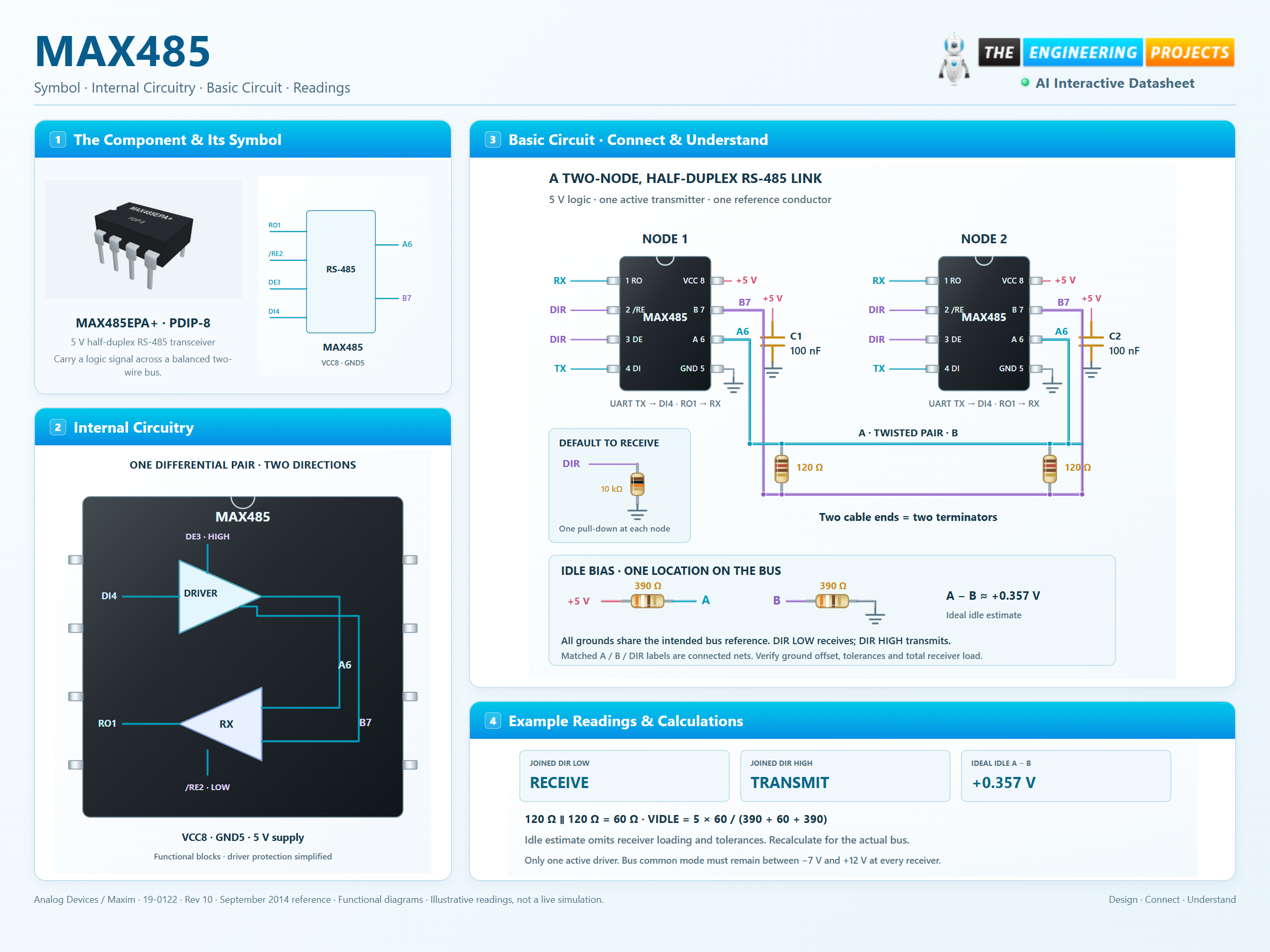
3 stages · Explore one step at a time
For the joined control, LOW enables the receiver and disables the driver. HIGH reverses those enable states.
DI HIGH makes A greater than B. DI LOW makes B greater than A. Only one node should actively drive.
The receiving node compares A − B with its thresholds. UART framing and error handling remain the controller’s job.
Physical transceivers, cable-end terminators and one bias network.
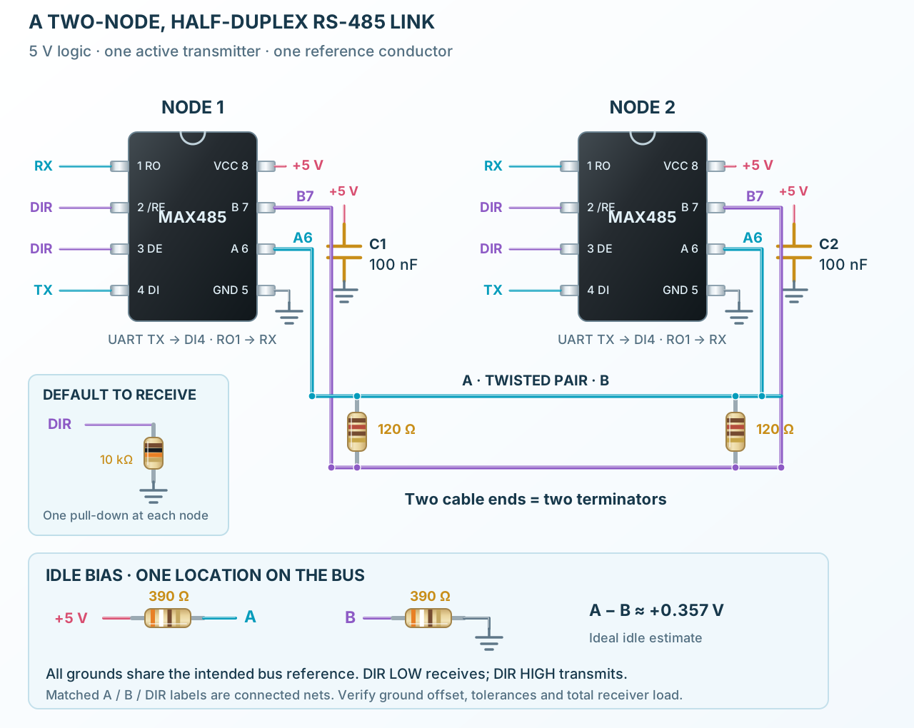
Follow the component values and pin connections
Connect TX, RX and direction to each transceiver. Use a receive-default pull-down.
Terminate only the two cable ends. The shown idle-bias pair is installed at one location.
Only one node transmits at a time. Wait for its final stop bit before releasing direction.
A differential driver and receiver share one bus pair.
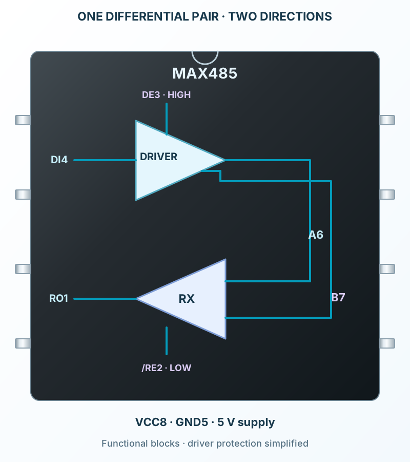
Select a stage to see its role and connections
DE enables the driver and DI selects differential polarity.
RE̅ LOW enables the receiver; HIGH makes RO high impedance.
Driver disable releases A/B. Arbitration and protocol timing are supplied by the system.
Signal names, electrical functions and connection guidance
Scroll within the table to see all columns and rows.
| Pin | Signal | Type | Function & connection |
|---|---|---|---|
| RO | Receiver data output | When enabled, HIGH for A − B ≥ 200 mV and LOW for A − B ≤ −200 mV. High impedance when RE̅ is HIGH.Connection guidanceConnect to a 5 V-compatible controller RX input. Open receiver inputs produce HIGH; a terminated idle bus needs separately designed bias. | |
| RE̅ | Active-LOW receiver enable | LOW enables RO; HIGH releases RO to high impedance.Connection guidanceJoin DE for one direction signal: LOW receive, HIGH transmit. | |
| DE | Active-HIGH driver enable | HIGH enables differential driver outputs; LOW releases the bus.Connection guidanceDrive from the direction GPIO; add a 10 kΩ pull-down for a receive-first startup. | |
| DI | Driver data input | With DE HIGH, DI HIGH makes A higher than B. DI LOW reverses the polarity.Connection guidanceConnect to controller UART TX. Logic HIGH ≥ 2.0 V; LOW ≤ 0.8 V. | |
| GND | Supply and signal reference | Reference for logic levels and bus common-mode voltage.Connection guidanceJoin the controller ground and the intended bus reference conductor. | |
| A | Non-inverting bus terminal | Non-inverting driver output and receiver input.Connection guidanceConnect A to A on the other node using a twisted pair. Receiver common-mode operating range −7 to +12 V. | |
| B | Inverting bus terminal | Inverting driver output and receiver input.Connection guidanceConnect B to B on the other node; verify vendor naming at third-party terminals. | |
| VCC | Regulated supply | Powers the transceiver from a nominal 5 V rail.Connection guidanceUse 4.75–5.25 V and 100 nF directly to pin 5. This is the 5 V MAX485, not a 3.3 V MAX3485. |
No pins match these filters. Try another signal name or reset the filters.
Controls are independent
Scroll within the table to see all columns and rows.
| Parameter | Value | Conditions / notes |
|---|---|---|
| DE HIGH; DI HIGH | A HIGH relative to B | Transmitter enabled |
| DE HIGH; DI LOW | A LOW relative to B | Transmitter enabled |
| DE LOW | A and B driver outputs high impedance | Receiver may remain enabled |
| RE̅ LOW; A − B ≥ +200 mV | RO HIGH | Within common-mode range |
| RE̅ LOW; A − B ≤ −200 mV | RO LOW | Within common-mode range |
| RE̅ HIGH | RO high impedance | External input may need a defined idle state |
| RE̅ LOW; both bus inputs open | RO HIGH | Specified open-input fail-safe |
| DE LOW; RE̅ HIGH | Driver and receiver disabled | MAX485 has no low-current shutdown mode |
No specifications match. Try a parameter name or a unit.
Do not assume a terminated, unbiased idle bus has the same fail-safe behavior as physically open receiver inputs.
Selected industrial grades
Scroll within the table to see all columns and rows.
| Parameter | Value | Conditions / notes |
|---|---|---|
| Supply voltage | 4.75–5.25 V | Nominal 5 V |
| Ambient range | −40 to +85°C | EPA / ESA orderables |
| Logic input HIGH / LOW | ≥ 2.0 V / ≤ 0.8 V | DI, DE and RE̅ |
| RO HIGH / LOW | ≥ 3.5 V / ≤ 0.4 V | Source / sink 4 mA |
| Receiver common-mode | −7 to +12 V | Referenced to local GND |
| Receiver threshold region | −200 to +200 mV | No guaranteed level inside the transition region |
| Typical input hysteresis | 70 mV | Common-mode 0 V |
| Receiver input resistance | 12 kΩ minimum | One standard unit load |
No specifications match. Try a parameter name or a unit.
A 3.3 V controller may drive the logic inputs, but its RX input must tolerate or translate the 5 V RO level.
Manufacturer specified test loads
Scroll within the table to see all columns and rows.
| Parameter | Value | Conditions / notes |
|---|---|---|
| Loaded differential output | 1.5 V minimum | RS-485 test load: two 27 Ω branches |
| No-load current, DE LOW | 300 µA typical; 500 µA maximum | MAX485; defined input levels |
| No-load current, DE HIGH | 500 µA typical; 900 µA maximum | MAX485; driver enabled and unloaded |
| Receiver bus loading | Up to 32 standard unit loads | Bias, cable and other loads also matter |
| Driver protection | Current limiting and thermal shutdown | Not permission for continuous bus contention |
| Slew-rate limiting | Not provided | Use controlled cable topology |
| Low-power shutdown | Not provided in MAX485 | MAX481 / 483 / 487 have different features |
No specifications match. Try a parameter name or a unit.
The MAX487 and MAX1487 quarter-unit-load and 128-node figures do not apply to MAX485.
5 V ±5% · manufacturer test circuits
Scroll within the table to see all columns and rows.
| Parameter | Value | Conditions / notes |
|---|---|---|
| Maximum data rate | 2.5 Mbit/s | Do not infer this rate over every cable length |
| Bit period at 2.5 Mbit/s | 400 ns | 1 / data rate |
| Driver propagation | 10–60 ns; 30 ns typical | 54 Ω differential load; 100 pF each output |
| Driver rise / fall | 3–40 ns; 15 ns typical | Specified test load |
| Receiver propagation | 200 ns maximum; 90 ns typical | 15 pF output load |
| Driver enable / disable | 70 ns maximum; 40 ns typical | Specified test circuits |
| Receiver enable / disable | 50 ns maximum; 20 ns typical | Specified test circuits |
No specifications match. Try a parameter name or a unit.
Protocol turnaround must also include UART completion, firmware latency, cable delay and the receiving node’s timing.
5 V controllers · short teaching link
Scroll within the table to see all columns and rows.
| Parameter | Value | Conditions / notes |
|---|---|---|
| UART TX / RX | TX → DI4; RO1 → RX | 5 V-compatible logic |
| Direction | GPIO → DE3 and RE̅2 | 10 kΩ pull-down: default receive |
| Twisted pair | A6 → A6; B7 → B7 | Keep stubs short |
| Cable-end termination | 120 Ω across A–B at each end | Two total; not at every node |
| Single idle-bias location | 390 Ω from +5 V to A; 390 Ω from B to GND | Example only; review loading and tolerances |
| Ideal idle difference | 5 × 60 / (390 + 60 + 390) ≈ 0.357 V | Two 120 Ω terminators in parallel; receiver loads omitted |
| Supply bypass | 100 nF at each IC, VCC8 to GND5 | Short local paths |
| Signal reference | Common reference conductor | Maintain each receiver’s common-mode limits |
No specifications match. Try a parameter name or a unit.
The bias estimate is a design illustration. Recalculate for actual transceiver count, tolerances, cable and ground offsets.
MAX485EPA+ · PDIP-8
Scroll within the table to see all columns and rows.
| Parameter | Value | Conditions / notes |
|---|---|---|
| PDIP-8 EPA | P8-1 · 2.54 mm pitch | 7.62 mm nominal lead rows |
| Narrow SOIC-8 ESA | S8-2 · 1.27 mm pitch | Separate surface-mount footprint |
| Supply absolute maximum | 12 V | Not the normal operating voltage |
| A / B absolute voltage | −8 to +12.5 V | Receiver operation remains −7 to +12 V common mode |
| Logic pin stress | −0.5 to VCC + 0.5 V | DI, enables and RO |
| PDIP dissipation at 70°C | 727 mW | Derate 9.09 mW/°C above 70°C |
| SOIC dissipation at 70°C | 471 mW | Derate 5.88 mW/°C above 70°C |
| Storage temperature | −65 to +160°C | Unpowered |
No specifications match. Try a parameter name or a unit.
The alternate µMAX package in this family uses a different pin arrangement and is not represented by these DIP/SO maps.
No matching rowsTry a pin name, parameter, unit or test condition, or reset the filters.
Carry a suitable serial protocol over a correctly terminated differential bus.
Manufacturer application guideShare one half-duplex pair with scheduled driver ownership.
Manufacturer application guideTranslate controller logic into RS-485 levels with reviewed grounding and protection.
Manufacturer application guideFind MAX485 in the Components Library to place its schematic symbol and connect its pins.
Reference page · circuit simulation model not yet availableOpen ProTech