MBR20100CTDual common-cathode Schottky rectifier
Two current paths. One shared positive output.
Manufacturer-referenced
Vishay General Semiconductor · MBR20100CT-E3
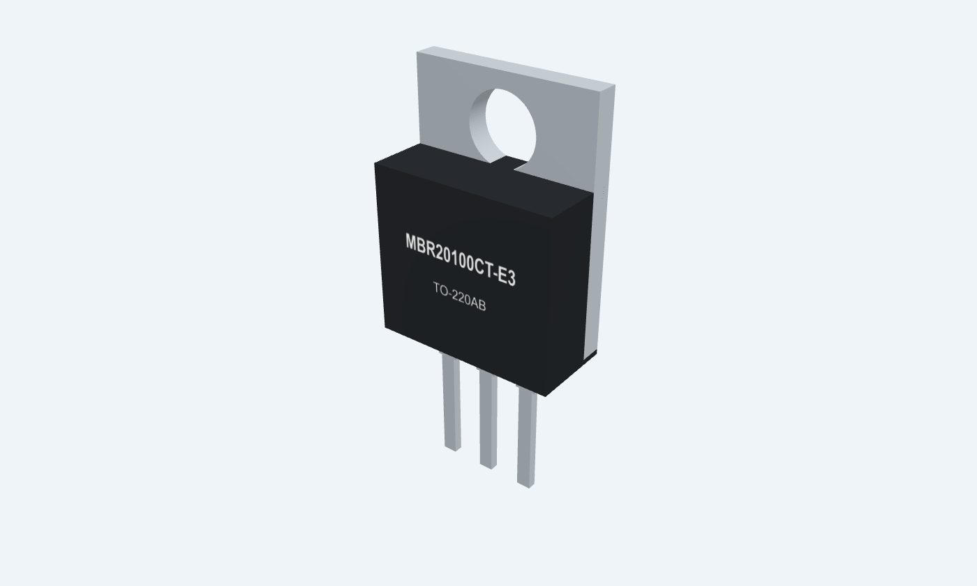
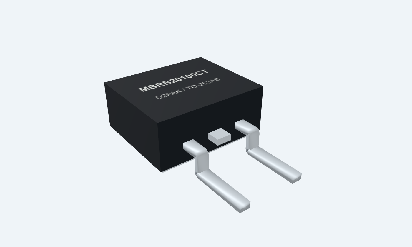
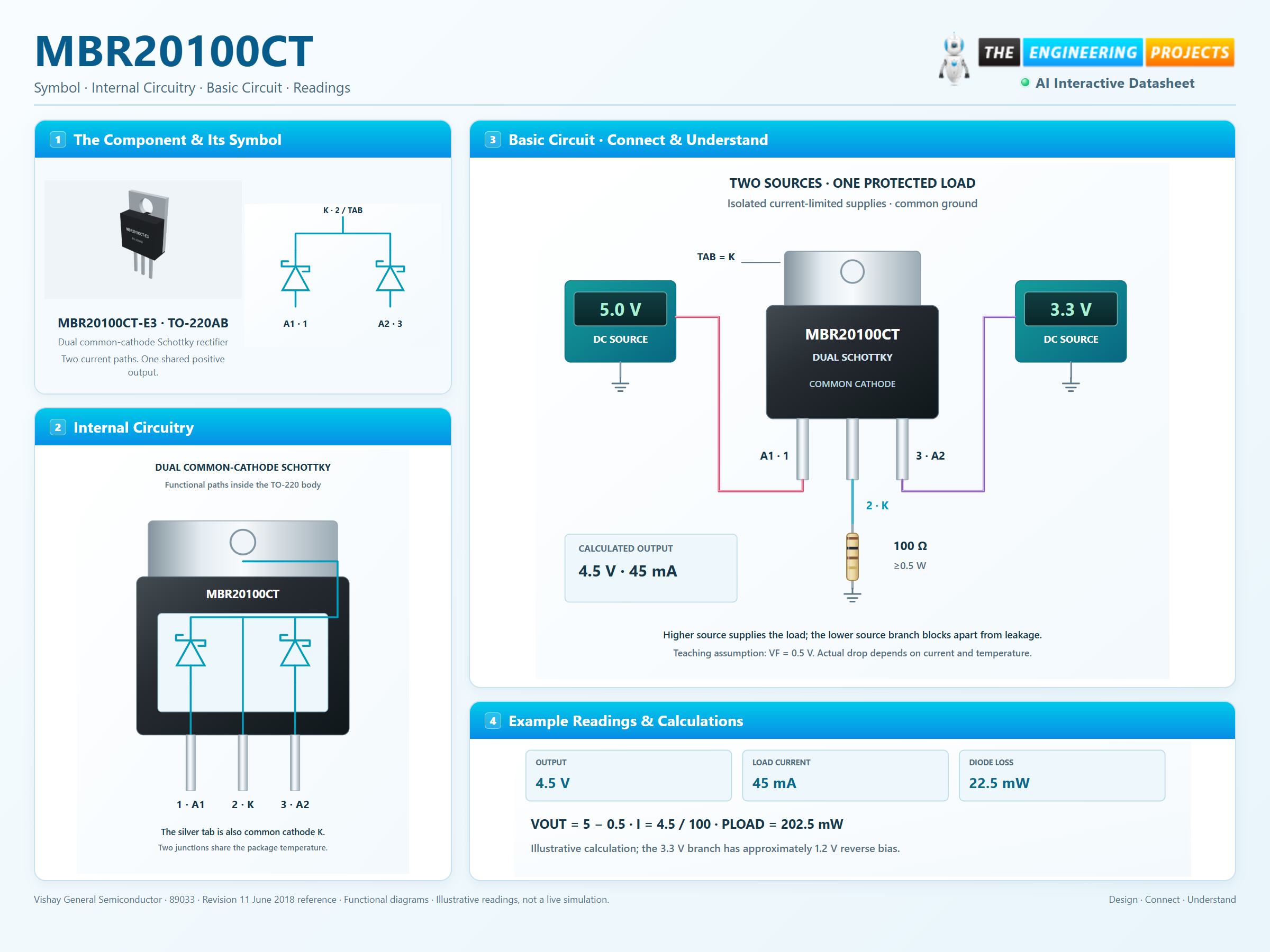
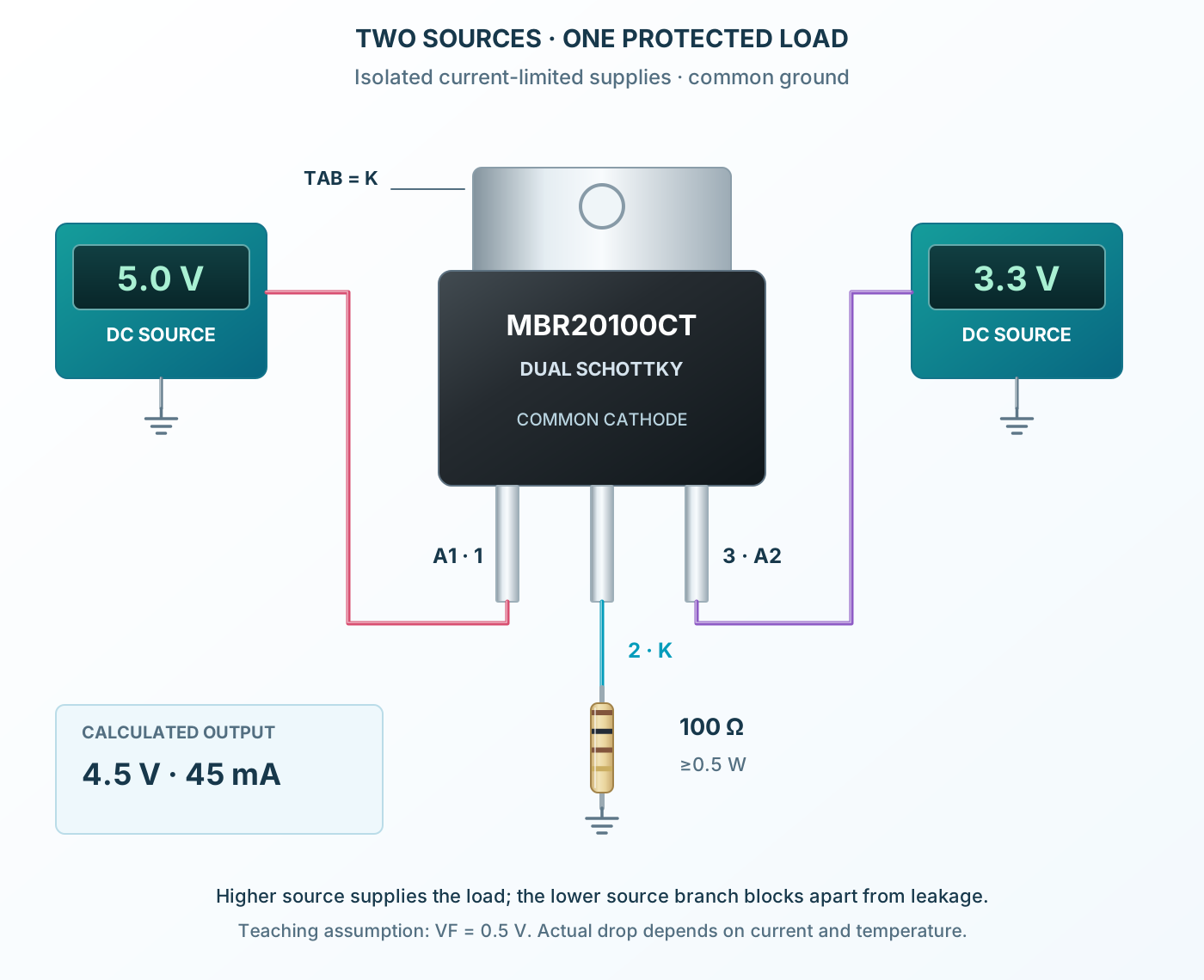
TO-220AB89033 · Revision 11 June 2018MBR20100CT contains two Schottky rectifiers with a common cathode. In the TO-220 front view, pin 1 is anode 1, pin 2 is the common cathode and pin 3 is anode 2. The exposed metal tab also connects to the cathode. The through-hole reference follows Vishay’s 100 V, 20 A total device; its 10 A per-diode rating requires the specified case temperature. The SMD switch shows Diodes Incorporated MBRB20100CT in D2PAK, a separately specified alternative with different thermal and leakage limits. The example combines current-limited 5 V and 3.3 V sources through the two anodes into a 100 Ω load. With an assumed 0.5 V conducting drop, the higher source gives about 4.5 V and 45 mA at the load. Both source negatives share ground.

3Physical pins
MBR20100CT-E3TO-220AB
Manufacturer-referencedVishay General Semiconductor
Pin diagram
Select a pin to explore its connection
Highlight
MBR20100CTTO-220ABFront view · A1, K2, A2 · tab = K2
MBR20100CTD2PAK / TO-263ABTop view · A1 left, A2 right, K2 metal pad
Click a lead or use the arrow keys. Front view · A1, K2, A2 · tab = K2
PIN 1 · Independent anodes
Anode 1A1
Function
Input to the first Schottky junction.
How to connect
Connect to the current-limited 5 V source in the example.
Electrical note
Each junction has its own current and thermal limits.
PIN 2 · Shared cathode / tab
Common cathodeK
Function
Both cathodes and the exposed metal tab share this node.
How to connect
Connect to the load positive. The load returns to the shared source ground.
Electrical note
The heatsink/tab is electrically live, not ground. Insulate it if required.
PIN 3 · Independent anodes
Anode 2A2
Function
Input to the second Schottky junction.
How to connect
Connect to the current-limited 3.3 V source in the example.
Electrical note
The higher available source normally supplies the load; equal sharing is not guaranteed.
Key specifications
Two junctions allow rectification or supply ORing. Heat, reverse leakage and the live tab still need attention.
Reverse voltage limit100 V · each diode
TO-220 total current20 A · case 133°C
Current per diode10 A · same case condition
TO-220 junction maximum150 °C · absolute limit
Package details
MBR20100CT-E3 · TO-220AB
| Property | Details |
|---|---|
| Manufacturer | Vishay General Semiconductor |
| Part number | MBR20100CT-E3 |
| Package | TO-220AB |
| Connections | 3 pins |
| Mounting | Through-hole |
| Lead pitch | 2.54 mm |
| Package code | TO220AB |
| Thermal reference | 20 A total at case 133°C; 150°C junction maximum |
Device and package selection
Two independently documented references
Manufacturer specifications 5 parameters
Scroll sideways to see all columns.
| Parameter | Value | Conditions / notes |
|---|---|---|
| Through-hole | Vishay MBR20100CT-E3 | TO-220AB |
| SMD | Diodes Incorporated MBRB20100CT | D2PAK / TO263AB |
| Pin functions | 1=A1; 2=K; 3=A2 | Both selected references |
| Metal tab | Common cathode | Not an isolated mounting surface |
| Architecture | Two Schottky junctions | Common cathode connection |
No specifications match. Try a parameter name or a unit.
Do not transfer temperature or thermal-resistance ratings between manufacturers.
TO-220 absolute maximum ratings
Vishay 89033, 100 V column
Manufacturer specifications 7 parameters
Scroll sideways to see all columns.
| Parameter | Value | Conditions / notes |
|---|---|---|
| Reverse peak / working / DC | 100 V | Each diode |
| Average current | 20 A total / 10 A per diode | Case 133°C |
| Forward surge | 150 A per diode | Single 8.3 ms half sine on rated load |
| Avalanche energy | 130 mJ per diode | TJ=25°C; L=60 mH |
| Repetitive reverse peak current | 0.5 A per diode | 2 µs; 1 kHz; TJ=38±2°C |
| Voltage slew | 10,000 V/µs | At rated reverse voltage |
| Junction / storage | −65 to +150°C | Absolute limits |
No specifications match. Try a parameter name or a unit.
The fully insulated MBRF variant is not the selected TO-220 device.
TO-220 electrical characteristics
Vishay per-diode limits
Manufacturer specifications 7 parameters
Scroll sideways to see all columns.
| Parameter | Value | Conditions / notes |
|---|---|---|
| Forward drop | 0.80 V maximum | 10 A; case 25°C |
| Hot forward drop | 0.65 V maximum | 10 A; case 125°C |
| High-current pulse drop | 0.75 V maximum | 20 A; case 125°C |
| Forward test | 300 µs; 1% duty | Avoid self-heating during measurement |
| Reverse leakage | 100 µA maximum | Rated reverse; TJ=25°C |
| Hot reverse leakage | 6 mA maximum | Rated reverse; TJ=125°C |
| Typical RθJC / RθJA | 2 / 60°C/W per diode | Manufacturer thermal reference |
No specifications match. Try a parameter name or a unit.
Check dissipation and cooling for both junctions, not only the total current label.
SMD electrical and thermal reference
Diodes DS37071, MBRB20100CT
Manufacturer specifications 8 parameters
Scroll sideways to see all columns.
| Parameter | Value | Conditions / notes |
|---|---|---|
| Reverse voltage | 100 V | Per leg |
| Average output | 10 A per leg / 20 A total | Half-wave 60 Hz resistive/inductive; derate capacitive loads 20% |
| Forward surge | 150 A | Single 8.3 ms half sine on rated load |
| Forward drop | 0.79 V typical; 0.84 V maximum | 10 A; TJ=25°C |
| Hot forward drop | 0.72 V maximum | 10 A; TJ=125°C |
| Reverse leakage | 0.1 mA / 10 mA maximum | 100 V; TJ=25 / 125°C |
| Typical RθJC / RθJA | 5 / 20°C/W | Tested with manufacturer’s 2-inch aluminum board |
| Junction / storage | −55 to +175°C | SMD reference only |
No specifications match. Try a parameter name or a unit.
Use the SMD PDF for its own derating curves and test setup.
Package and PCB geometry
Dimensions before assembly
Manufacturer specifications 7 parameters
Scroll sideways to see all columns.
| Parameter | Value | Conditions / notes |
|---|---|---|
| TO-220 lead pitch | 2.45–2.65 mm | Nominal 2.54 mm |
| TO-220 body width | 9.65–10.54 mm | Vishay outline |
| TO-220 lead width / thickness | 0.70–0.90 / 0.36–0.56 mm | Vishay outline |
| Authored through-hole pads | 2.2 mm copper; 1.2 mm holes | Engineering layout choice |
| SMD cathode land | 10.41 × 7.01 mm | Diodes suggested layout |
| SMD anode lands | 1.10 × 3.50 mm | 5.08 mm centers |
| SMD overall land span | 15.99 mm | From cathode land top to anode land bottom |
No specifications match. Try a parameter name or a unit.
Check the actual package revision, heatsink and PCB assembly process.
Supply ORing example
Isolated low-voltage teaching circuit
Manufacturer specifications 6 parameters
Scroll sideways to see all columns.
| Parameter | Value | Conditions / notes |
|---|---|---|
| Sources | 5 V and 3.3 V DC | Both current limited; shared ground |
| Load | 100 Ω; at least 0.5 W | Connected to common cathode |
| Assumed forward drop | 0.5 V | Not a guaranteed operating value |
| Output / load current | 4.5 V / 45 mA | Higher source supplies load |
| Load / diode dissipation | 202.5 / 22.5 mW | Fixed-drop calculation |
| Lower-source branch | Approximately 1.2 V reverse bias | Leakage remains; not a perfect disconnect |
No specifications match. Try a parameter name or a unit.
This is not an ideal-diode controller and does not guarantee equal current sharing.
Connections by function
Select a pin for its function, connection guidance and electrical notes.
Independent anodes2 pins
Shared cathode / tab1 pin
Independent anodes2 pins
Shared cathode / tab1 pin
MBR20100CT at a glance
Follow the labeled connections and functional stages
How it works
3 stages · Explore one step at a time
Identify the shared output
Pin 2 and the metal tab are the common cathode.
Apply the two inputs
Current-limited sources connect to anodes 1 and 3, with their negatives joined.
Follow the higher source
The higher anode voltage supplies the load through its forward-biased junction; the other branch blocks apart from leakage.
Step 1 of 3
MBR20100CT in a circuit
A physical dual diode, clear wiring and shared ground.
Connect it, step by step
Follow the component values and pin connections
Connect the inputs
5 V to pin 1 and 3.3 V to pin 3.
Connect the load
Pin 2 feeds the 100 Ω load.
Join the returns
Both source negatives and the load return share ground.
Inside MBR20100CT
Compact common-cathode topology inside the body.
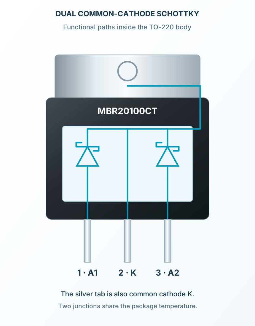
Explore the circuit
Select a stage to see its role and connections
Independent anodes
Each anode enters a separate rectifying junction.
Shared cathode
Both cathodes join the central output and metal tab.
Shared heating
Dissipation in either junction affects the package temperature.
Selected packageTO-220ABMBR20100CT-E3
Physical connections3 pinsPackage-specific numbering
Reference collection7 tables40 parameters & pin functions
Pin reference
Signal names, electrical functions and connection guidance
Physical pin numbers3 pins
Scroll within the table to see all columns and rows.
| Pin | Signal | Type | Function & connection |
|---|---|---|---|
| A1 | Anode 1 | Input to the first Schottky junction.Connection guidanceConnect to the current-limited 5 V source in the example. Each junction has its own current and thermal limits. | |
| K | Common cathode | Both cathodes and the exposed metal tab share this node.Connection guidanceConnect to the load positive. The load returns to the shared source ground. The heatsink/tab is electrically live, not ground. Insulate it if required. | |
| A2 | Anode 2 | Input to the second Schottky junction.Connection guidanceConnect to the current-limited 3.3 V source in the example. The higher available source normally supplies the load; equal sharing is not guaranteed. |
No pins match these filters. Try another signal name or reset the filters.
Device and package selection
Two independently documented references
Manufacturer-referenced values5 parameters
Scroll within the table to see all columns and rows.
| Parameter | Value | Conditions / notes |
|---|---|---|
| Through-hole | Vishay MBR20100CT-E3 | TO-220AB |
| SMD | Diodes Incorporated MBRB20100CT | D2PAK / TO263AB |
| Pin functions | 1=A1; 2=K; 3=A2 | Both selected references |
| Metal tab | Common cathode | Not an isolated mounting surface |
| Architecture | Two Schottky junctions | Common cathode connection |
No specifications match. Try a parameter name or a unit.
Do not transfer temperature or thermal-resistance ratings between manufacturers.
TO-220 absolute maximum ratings
Vishay 89033, 100 V column
Manufacturer-referenced values7 parameters
Scroll within the table to see all columns and rows.
| Parameter | Value | Conditions / notes |
|---|---|---|
| Reverse peak / working / DC | 100 V | Each diode |
| Average current | 20 A total / 10 A per diode | Case 133°C |
| Forward surge | 150 A per diode | Single 8.3 ms half sine on rated load |
| Avalanche energy | 130 mJ per diode | TJ=25°C; L=60 mH |
| Repetitive reverse peak current | 0.5 A per diode | 2 µs; 1 kHz; TJ=38±2°C |
| Voltage slew | 10,000 V/µs | At rated reverse voltage |
| Junction / storage | −65 to +150°C | Absolute limits |
No specifications match. Try a parameter name or a unit.
The fully insulated MBRF variant is not the selected TO-220 device.
TO-220 electrical characteristics
Vishay per-diode limits
Manufacturer-referenced values7 parameters
Scroll within the table to see all columns and rows.
| Parameter | Value | Conditions / notes |
|---|---|---|
| Forward drop | 0.80 V maximum | 10 A; case 25°C |
| Hot forward drop | 0.65 V maximum | 10 A; case 125°C |
| High-current pulse drop | 0.75 V maximum | 20 A; case 125°C |
| Forward test | 300 µs; 1% duty | Avoid self-heating during measurement |
| Reverse leakage | 100 µA maximum | Rated reverse; TJ=25°C |
| Hot reverse leakage | 6 mA maximum | Rated reverse; TJ=125°C |
| Typical RθJC / RθJA | 2 / 60°C/W per diode | Manufacturer thermal reference |
No specifications match. Try a parameter name or a unit.
Check dissipation and cooling for both junctions, not only the total current label.
SMD electrical and thermal reference
Diodes DS37071, MBRB20100CT
Manufacturer-referenced values8 parameters
Scroll within the table to see all columns and rows.
| Parameter | Value | Conditions / notes |
|---|---|---|
| Reverse voltage | 100 V | Per leg |
| Average output | 10 A per leg / 20 A total | Half-wave 60 Hz resistive/inductive; derate capacitive loads 20% |
| Forward surge | 150 A | Single 8.3 ms half sine on rated load |
| Forward drop | 0.79 V typical; 0.84 V maximum | 10 A; TJ=25°C |
| Hot forward drop | 0.72 V maximum | 10 A; TJ=125°C |
| Reverse leakage | 0.1 mA / 10 mA maximum | 100 V; TJ=25 / 125°C |
| Typical RθJC / RθJA | 5 / 20°C/W | Tested with manufacturer’s 2-inch aluminum board |
| Junction / storage | −55 to +175°C | SMD reference only |
No specifications match. Try a parameter name or a unit.
Use the SMD PDF for its own derating curves and test setup.
Package and PCB geometry
Dimensions before assembly
Manufacturer-referenced values7 parameters
Scroll within the table to see all columns and rows.
| Parameter | Value | Conditions / notes |
|---|---|---|
| TO-220 lead pitch | 2.45–2.65 mm | Nominal 2.54 mm |
| TO-220 body width | 9.65–10.54 mm | Vishay outline |
| TO-220 lead width / thickness | 0.70–0.90 / 0.36–0.56 mm | Vishay outline |
| Authored through-hole pads | 2.2 mm copper; 1.2 mm holes | Engineering layout choice |
| SMD cathode land | 10.41 × 7.01 mm | Diodes suggested layout |
| SMD anode lands | 1.10 × 3.50 mm | 5.08 mm centers |
| SMD overall land span | 15.99 mm | From cathode land top to anode land bottom |
No specifications match. Try a parameter name or a unit.
Check the actual package revision, heatsink and PCB assembly process.
Supply ORing example
Isolated low-voltage teaching circuit
Manufacturer-referenced values6 parameters
Scroll within the table to see all columns and rows.
| Parameter | Value | Conditions / notes |
|---|---|---|
| Sources | 5 V and 3.3 V DC | Both current limited; shared ground |
| Load | 100 Ω; at least 0.5 W | Connected to common cathode |
| Assumed forward drop | 0.5 V | Not a guaranteed operating value |
| Output / load current | 4.5 V / 45 mA | Higher source supplies load |
| Load / diode dissipation | 202.5 / 22.5 mW | Fixed-drop calculation |
| Lower-source branch | Approximately 1.2 V reverse bias | Leakage remains; not a perfect disconnect |
No specifications match. Try a parameter name or a unit.
This is not an ideal-diode controller and does not guarantee equal current sharing.
No matching rowsTry a pin name, parameter, unit or test condition, or reset the filters.
Supply ORing
Combine compatible positive sources while limiting reverse feed between them.
Manufacturer application guideRectifier circuits
Use the common-cathode topology in a suitable low-voltage converter or center-tapped rectifier.
Manufacturer application guideFreewheel paths
Select polarity, current and energy margins for the actual switching circuit.
Manufacturer application guideTake it into ProTech
Find MBR20100CT in the Components Library to place its schematic symbol and connect its pins.
Reference page · circuit simulation model not yet availableOpen ProTech