Real View
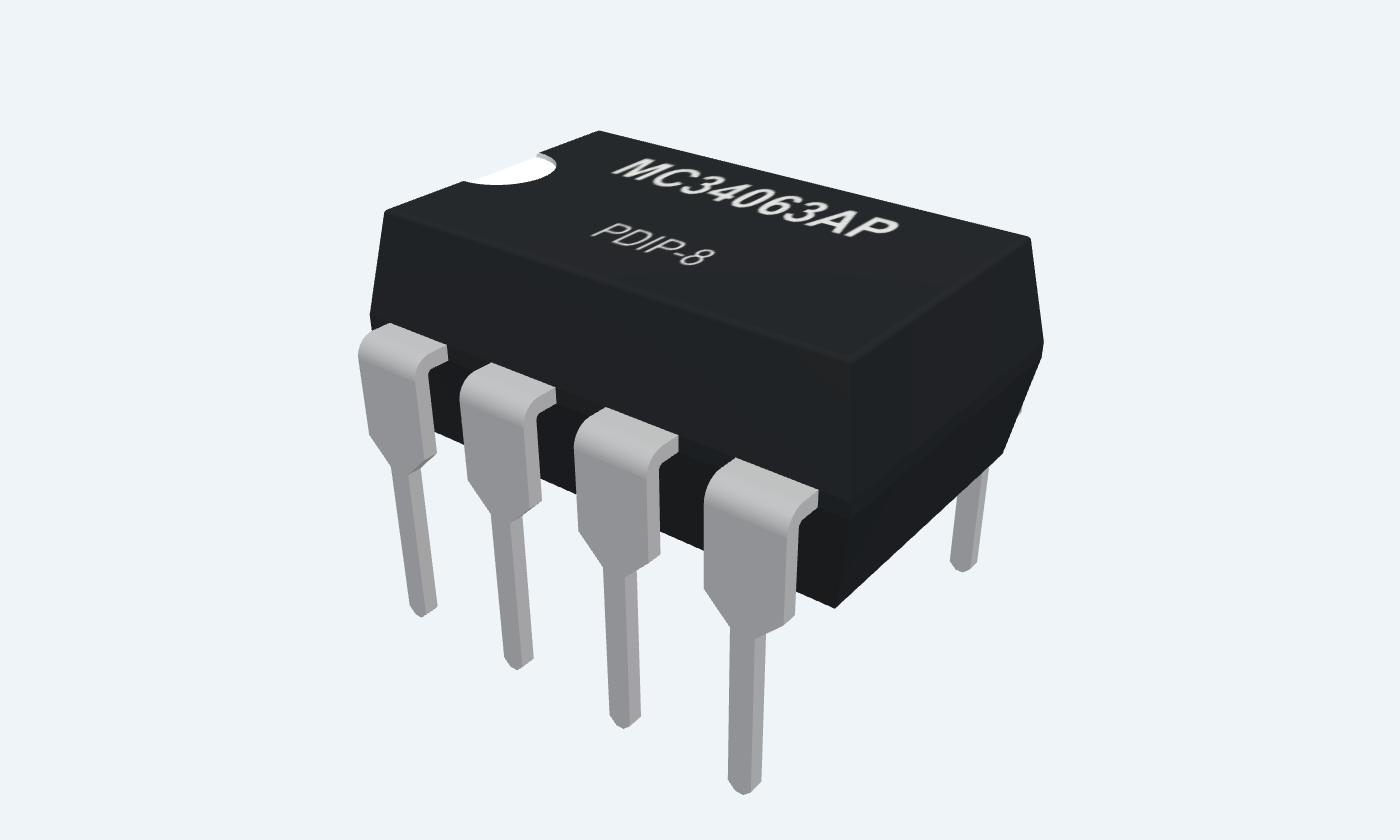
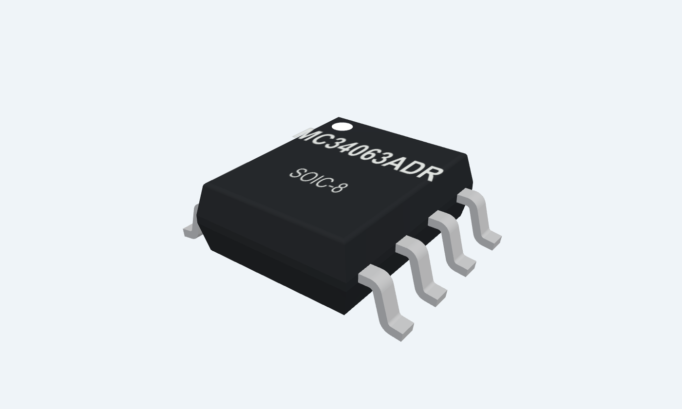
One switching controller. Three ways to change a DC rail.
MC34063A is an eight-pin switching controller with an internal NPN power switch, reference, comparator, oscillator and current-limit circuit. External connections configure it as a buck, boost or inverting converter. Its 1.5 A headline rating describes peak switch current. Available output current depends on topology, voltage ratio, inductor ripple and cooling; a boost output cannot simply deliver 1.5 A at every voltage. This reference follows TI’s commercial 0–70°C MC34063A in PDIP-8 and SOIC-8. The illustrated buck circuit follows the manufacturer’s example, with its resistor-selected output and distinct current-sense, timing and feedback nodes.
Select a pin to explore its connection
Click a lead or use the arrow keys. Top view
Collector of the internal high-current NPN switch.
In the buck example, connect to the current-sense resistor output and driver collector pin 8.
The 1.5 A rating is a peak switch limit, not a guaranteed load current.
Emitter of the internal output switch.
In the buck circuit, connect to L1 and the catch-diode cathode.
This is a switching node, not the filtered DC output.
An external capacitor sets the oscillator timing.
Connect the 470 pF example capacitor from CT to GND.
The 33 kHz typical specification is measured with CT = 1 nF; do not assign it to every timing capacitor.
Return for the reference, oscillator and comparator.
Join the input/output capacitor returns and diode anode with short power paths.
Keep the feedback return away from large switching currents.
Compares the output-divider voltage with the internal 1.25 V reference.
Connect to the junction of R2 from output and R1 to ground.
Output setting is approximately 1.25 × (1 + R2/R1).
Supplies the control circuitry.
Connect to VIN before the current-sense resistor and bypass locally.
Recommended supply range 3–40 V; the example uses 25 V.
Senses the drop between the supply and the current-sense node.
Connect after RSC, at the switch/driver collector feed.
Approximately 300 mV across RSC invokes current limiting; 250–350 mV at 25°C.
Collector supply of the internal driver transistor.
Join to pin 1 after RSC in this Darlington buck configuration.
Alternative driver configurations need the manufacturer’s base-drive design checks.
The external inductor and diode carry the energy. CT controls timing, RSC limits peak current and the output divider sets the regulated voltage.
MC34063AP · PDIP-8
| Property | Details |
|---|---|
| Manufacturer | Texas Instruments |
| Part number | MC34063AP |
| Package | PDIP-8 |
| Connections | 8 pins |
| Mounting | Through-hole |
| Lead pitch | 2.54 mm |
| Package code | dip |
| Thermal reference | Board and package dependent; see manufacturer data |
Selected commercial MC34063A
Scroll sideways to see all columns.
| Parameter | Value | Conditions / notes |
|---|---|---|
| Supply | 3–40 V | Recommended VCC range |
| Ambient temperature | 0 to +70°C | MC34063A; MC33063A is a separately specified −40 to +85°C option |
| Topologies | Buck / boost / inverting | External wiring and calculations differ |
| Maximum oscillator capability | 100 kHz | External CT and the operating conditions determine actual timing |
| Peak switch current | 1.5 A | Not a guaranteed continuous load current |
| Packages shown | PDIP-8 / SOIC-8 | TI P / D orderables |
No specifications match. Try a parameter name or a unit.
Keep voltage overshoot and thermal stress within the exact device ratings.
VCC = 5 V; TA = 25°C unless noted
Scroll sideways to see all columns.
| Parameter | Value | Conditions / notes |
|---|---|---|
| Frequency with CT = 1 nF | 24 / 33 / 42 kHz | Minimum / typical / maximum; pin 5 at 0 V |
| Capacitor charge current | 24 / 35 / 42 µA | VCC = 5–40 V |
| Capacitor discharge current | 140 / 220 / 260 µA | VCC = 5–40 V |
| Discharge / charge ratio | 5.2 / 6.5 / 7.5 | Pin 7 tied to VCC |
| Current-limit sense voltage | 250 / 300 / 350 mV | Characterized at equal charge and discharge currents |
| Nominal sense resistor | RSC ≈ 0.3 / IPEAK | Use threshold tolerance and waveform margins |
No specifications match. Try a parameter name or a unit.
The CT = 1 nF frequency is a test point, not the frequency of the illustrated 470 pF circuit.
TI electrical-characteristic conditions
Scroll sideways to see all columns.
| Parameter | Value | Conditions / notes |
|---|---|---|
| Reference at 25°C | 1.225 / 1.250 / 1.275 V | Minimum / typical / maximum |
| Reference over ambient range | 1.21–1.29 V | Commercial operating range |
| Reference line change | 1.4 mV typical; 5 mV maximum | VCC = 5–40 V |
| Darlington switch saturation | 1 V typical; 1.3 V maximum | ISW = 1 A; pins 1 and 8 joined |
| Non-Darlington saturation | 0.45 V typical; 0.7 V maximum | ISW = 1 A, 82 Ω driver feed, forced beta about 20 |
| Supply current | 4 mA maximum | VCC = 5–40 V; output-switch-off test conditions |
No specifications match. Try a parameter name or a unit.
Driver topology changes switching loss and turn-off behavior. Use the complete manufacturer conditions.
TI Figure 11 · 25 V input, approximately 5 V output
Scroll sideways to see all columns.
| Parameter | Value | Conditions / notes |
|---|---|---|
| RSC | 0.33 Ω | Between VIN and the joined SC1 / IPK7 / DC8 feed |
| CT | 470 pF | Pin 3 to ground |
| L1 | 220 µH | Pin 2 to filtered output; select suitable saturation and RMS ratings |
| Catch diode | 1N5819 | Cathode at pin 2; anode at GND |
| CIN / COUT | 100 µF / 470 µF | Choose voltage/ripple ratings and suitable ESR; illustrated 50 V / 16 V |
| R2 / R1 | 3.8 kΩ / 1.2 kΩ | R2 from output to INV5; R1 from INV5 to GND |
| Reference load | 500 mA | Manufacturer application example, not the part’s universal current rating |
No specifications match. Try a parameter name or a unit.
The optional extra LC output filter is omitted from the illustration. The nominal resistor ratio gives 5.208 V before tolerance and losses.
Calculated illustrations
Scroll sideways to see all columns.
| Parameter | Value | Conditions / notes |
|---|---|---|
| Divider output | 5.208 V | 1.25 × (1 + 3.8/1.2) |
| Nominal current limit | 0.909 A | 0.300 V / 0.33 Ω |
| Threshold-only limit interval | 0.758–1.061 A | 0.250–0.350 V / 0.33 Ω; excludes resistor tolerance and dynamic effects |
| Ideal duty at 25 V | 20.8% | 5.208 / 25; excludes switch/diode drops |
| Output power at 0.5 A | Approximately 2.60 W | 5.208 V × 0.5 A |
| Simple resistor load | About 10.4 Ω | For an illustrative 0.5 A load; rate it above the dissipated power |
No specifications match. Try a parameter name or a unit.
These calculations explain the circuit. They are not live measurements or a switching simulation.
Protect quiet nodes from switching currents
Scroll sideways to see all columns.
| Parameter | Value | Conditions / notes |
|---|---|---|
| Current-sense path | VIN6 → RSC → IPK7 / SC1 / DC8 | Use short, low-inductance paths and sense the resistor terminals |
| Switch node | SE2 → L1 and diode cathode | Keep copper compact |
| Catch path | GND → diode → SE2 → L1 | Short loop with the output capacitor |
| Feedback divider | Output → R2 → INV5 → R1 → GND | Route away from switch-node copper |
| Timing capacitor | CT3 → GND4 | Place close to the IC |
| Physical package mapping | Eight pins in both selected packages | Pin 1 indication remains visible |
No specifications match. Try a parameter name or a unit.
Changing from buck to boost or inverting operation requires a different power-stage connection.
Absolute maxima are not normal targets
Scroll sideways to see all columns.
| Parameter | Value | Conditions / notes |
|---|---|---|
| Supply / switch voltage | 40 V | Absolute limits require checking each referenced voltage |
| Driver collector current | 100 mA | Absolute maximum |
| Switch current | 1.5 A | Absolute maximum |
| Junction temperature | 150°C | Absolute maximum; thermal design must stay below it |
| Storage temperature | −65 to +150°C | Unpowered |
| Comparator input | −0.3 to +40 V | Absolute input range, not a desired feedback voltage |
No specifications match. Try a parameter name or a unit.
A headline current rating cannot replace dissipation and temperature calculations.
Select a pin for its function, connection guidance and electrical notes.
Follow the labeled connections and functional stages
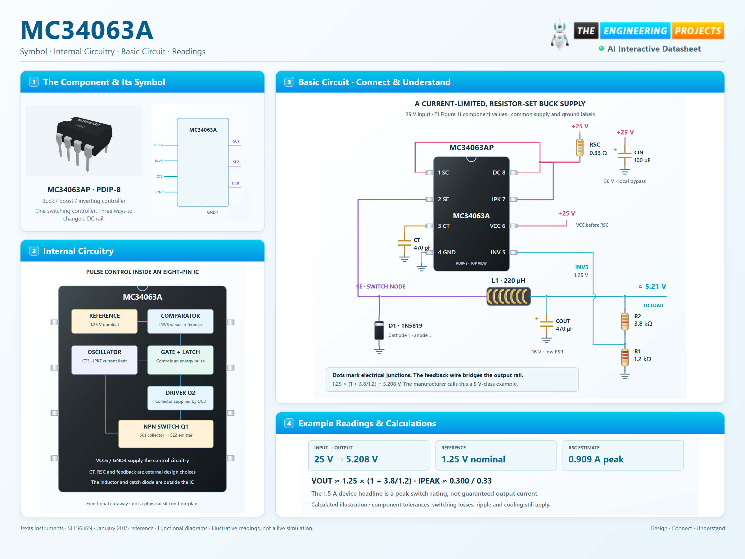
3 stages · Explore one step at a time
The timing capacitor controls the oscillator. When feedback requests energy, the driver turns the output switch on.
The drop across RSC increases with switch-path current. The sense circuit changes the timing when its threshold is reached.
Pin 5 compares the divided output against 1.25 V. The inductor and catch diode continue supplying current between switching pulses.
Physical PDIP-8 · 25 V input · resistor-set output.
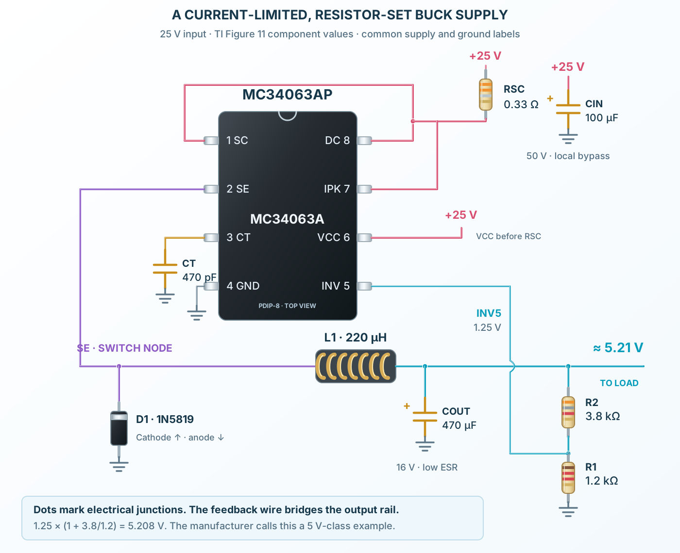
Follow the component values and pin connections
Feed VCC6 before RSC, with SC1, IPK7 and DC8 after it.
SE2 feeds the inductor. The diode carries off-state current from ground.
The R2/R1 junction drives INV5. The nominal divider predicts 5.208 V.
Timing, feedback and switch drive within the eight-pin package.
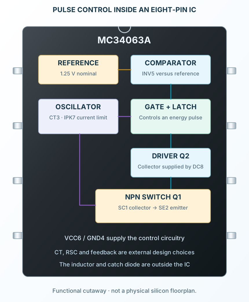
Select a stage to see its role and connections
INV5 is compared with the 1.25 V reference.
CT3 and IPK7 feed the pulse-control system.
DC8 supplies the driver; SC1 and SE2 expose the main switch terminals.
Signal names, electrical functions and connection guidance
Scroll within the table to see all columns and rows.
| Pin | Signal | Type | Function & connection |
|---|---|---|---|
| SC | Switch collector | Collector of the internal high-current NPN switch.Connection guidanceIn the buck example, connect to the current-sense resistor output and driver collector pin 8. The 1.5 A rating is a peak switch limit, not a guaranteed load current. | |
| SE | Switch emitter | Emitter of the internal output switch.Connection guidanceIn the buck circuit, connect to L1 and the catch-diode cathode. This is a switching node, not the filtered DC output. | |
| CT | Timing capacitor | An external capacitor sets the oscillator timing.Connection guidanceConnect the 470 pF example capacitor from CT to GND. The 33 kHz typical specification is measured with CT = 1 nF; do not assign it to every timing capacitor. | |
| GND | Common return | Return for the reference, oscillator and comparator.Connection guidanceJoin the input/output capacitor returns and diode anode with short power paths. Keep the feedback return away from large switching currents. | |
| INV | Comparator inverting input | Compares the output-divider voltage with the internal 1.25 V reference.Connection guidanceConnect to the junction of R2 from output and R1 to ground. Output setting is approximately 1.25 × (1 + R2/R1). | |
| VCC | Control supply | Supplies the control circuitry.Connection guidanceConnect to VIN before the current-sense resistor and bypass locally. Recommended supply range 3–40 V; the example uses 25 V. | |
| IPK | Peak current sense | Senses the drop between the supply and the current-sense node.Connection guidanceConnect after RSC, at the switch/driver collector feed. Approximately 300 mV across RSC invokes current limiting; 250–350 mV at 25°C. | |
| DC | Driver collector | Collector supply of the internal driver transistor.Connection guidanceJoin to pin 1 after RSC in this Darlington buck configuration. Alternative driver configurations need the manufacturer’s base-drive design checks. |
No pins match these filters. Try another signal name or reset the filters.
Selected commercial MC34063A
Scroll within the table to see all columns and rows.
| Parameter | Value | Conditions / notes |
|---|---|---|
| Supply | 3–40 V | Recommended VCC range |
| Ambient temperature | 0 to +70°C | MC34063A; MC33063A is a separately specified −40 to +85°C option |
| Topologies | Buck / boost / inverting | External wiring and calculations differ |
| Maximum oscillator capability | 100 kHz | External CT and the operating conditions determine actual timing |
| Peak switch current | 1.5 A | Not a guaranteed continuous load current |
| Packages shown | PDIP-8 / SOIC-8 | TI P / D orderables |
No specifications match. Try a parameter name or a unit.
Keep voltage overshoot and thermal stress within the exact device ratings.
VCC = 5 V; TA = 25°C unless noted
Scroll within the table to see all columns and rows.
| Parameter | Value | Conditions / notes |
|---|---|---|
| Frequency with CT = 1 nF | 24 / 33 / 42 kHz | Minimum / typical / maximum; pin 5 at 0 V |
| Capacitor charge current | 24 / 35 / 42 µA | VCC = 5–40 V |
| Capacitor discharge current | 140 / 220 / 260 µA | VCC = 5–40 V |
| Discharge / charge ratio | 5.2 / 6.5 / 7.5 | Pin 7 tied to VCC |
| Current-limit sense voltage | 250 / 300 / 350 mV | Characterized at equal charge and discharge currents |
| Nominal sense resistor | RSC ≈ 0.3 / IPEAK | Use threshold tolerance and waveform margins |
No specifications match. Try a parameter name or a unit.
The CT = 1 nF frequency is a test point, not the frequency of the illustrated 470 pF circuit.
TI electrical-characteristic conditions
Scroll within the table to see all columns and rows.
| Parameter | Value | Conditions / notes |
|---|---|---|
| Reference at 25°C | 1.225 / 1.250 / 1.275 V | Minimum / typical / maximum |
| Reference over ambient range | 1.21–1.29 V | Commercial operating range |
| Reference line change | 1.4 mV typical; 5 mV maximum | VCC = 5–40 V |
| Darlington switch saturation | 1 V typical; 1.3 V maximum | ISW = 1 A; pins 1 and 8 joined |
| Non-Darlington saturation | 0.45 V typical; 0.7 V maximum | ISW = 1 A, 82 Ω driver feed, forced beta about 20 |
| Supply current | 4 mA maximum | VCC = 5–40 V; output-switch-off test conditions |
No specifications match. Try a parameter name or a unit.
Driver topology changes switching loss and turn-off behavior. Use the complete manufacturer conditions.
TI Figure 11 · 25 V input, approximately 5 V output
Scroll within the table to see all columns and rows.
| Parameter | Value | Conditions / notes |
|---|---|---|
| RSC | 0.33 Ω | Between VIN and the joined SC1 / IPK7 / DC8 feed |
| CT | 470 pF | Pin 3 to ground |
| L1 | 220 µH | Pin 2 to filtered output; select suitable saturation and RMS ratings |
| Catch diode | 1N5819 | Cathode at pin 2; anode at GND |
| CIN / COUT | 100 µF / 470 µF | Choose voltage/ripple ratings and suitable ESR; illustrated 50 V / 16 V |
| R2 / R1 | 3.8 kΩ / 1.2 kΩ | R2 from output to INV5; R1 from INV5 to GND |
| Reference load | 500 mA | Manufacturer application example, not the part’s universal current rating |
No specifications match. Try a parameter name or a unit.
The optional extra LC output filter is omitted from the illustration. The nominal resistor ratio gives 5.208 V before tolerance and losses.
Calculated illustrations
Scroll within the table to see all columns and rows.
| Parameter | Value | Conditions / notes |
|---|---|---|
| Divider output | 5.208 V | 1.25 × (1 + 3.8/1.2) |
| Nominal current limit | 0.909 A | 0.300 V / 0.33 Ω |
| Threshold-only limit interval | 0.758–1.061 A | 0.250–0.350 V / 0.33 Ω; excludes resistor tolerance and dynamic effects |
| Ideal duty at 25 V | 20.8% | 5.208 / 25; excludes switch/diode drops |
| Output power at 0.5 A | Approximately 2.60 W | 5.208 V × 0.5 A |
| Simple resistor load | About 10.4 Ω | For an illustrative 0.5 A load; rate it above the dissipated power |
No specifications match. Try a parameter name or a unit.
These calculations explain the circuit. They are not live measurements or a switching simulation.
Protect quiet nodes from switching currents
Scroll within the table to see all columns and rows.
| Parameter | Value | Conditions / notes |
|---|---|---|
| Current-sense path | VIN6 → RSC → IPK7 / SC1 / DC8 | Use short, low-inductance paths and sense the resistor terminals |
| Switch node | SE2 → L1 and diode cathode | Keep copper compact |
| Catch path | GND → diode → SE2 → L1 | Short loop with the output capacitor |
| Feedback divider | Output → R2 → INV5 → R1 → GND | Route away from switch-node copper |
| Timing capacitor | CT3 → GND4 | Place close to the IC |
| Physical package mapping | Eight pins in both selected packages | Pin 1 indication remains visible |
No specifications match. Try a parameter name or a unit.
Changing from buck to boost or inverting operation requires a different power-stage connection.
Absolute maxima are not normal targets
Scroll within the table to see all columns and rows.
| Parameter | Value | Conditions / notes |
|---|---|---|
| Supply / switch voltage | 40 V | Absolute limits require checking each referenced voltage |
| Driver collector current | 100 mA | Absolute maximum |
| Switch current | 1.5 A | Absolute maximum |
| Junction temperature | 150°C | Absolute maximum; thermal design must stay below it |
| Storage temperature | −65 to +150°C | Unpowered |
| Comparator input | −0.3 to +40 V | Absolute input range, not a desired feedback voltage |
No specifications match. Try a parameter name or a unit.
A headline current rating cannot replace dissipation and temperature calculations.
No matching rowsTry a pin name, parameter, unit or test condition, or reset the filters.
Create a lower-voltage supply using the emitter switch node, inductor and catch diode.
Manufacturer application guideRewire the power stage for boost operation and calculate switch current from the higher voltage ratio.
Manufacturer application guideUse the inverting topology with appropriate grounding, component stress and feedback design.
Manufacturer application guideFind MC34063A in the Components Library to place its schematic symbol and connect its pins.
Reference page · circuit simulation model not yet availableOpen ProTech