MCP2515Stand-alone CAN controller with SPI
Add classical CAN messaging to an SPI-equipped controller.
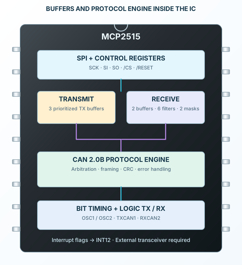
MCP2515 is a stand-alone classical CAN 2.0B controller accessed through SPI. It handles frame formatting, arbitration, error detection and message buffering, while the host prepares messages and services received data. An external transceiver is required to drive CANH and CANL. Three transmit buffers and two receive buffers separate bus activity from host transfers. Six acceptance filters and two masks can reduce unnecessary host work. Standard 11-bit identifiers and extended 29-bit identifiers are supported, with up to eight data bytes per frame; CAN FD is not supported. The example combines a 5 V controller, a 20 MHz external oscillator and an MCP2562 transceiver. A reviewed timing setup produces 125 kbit/s. Wiring alone does not start communication: firmware must reset and configure the controller, select Normal mode and communicate with another correctly configured node.
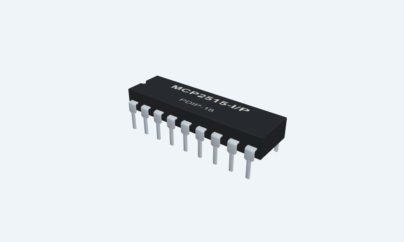
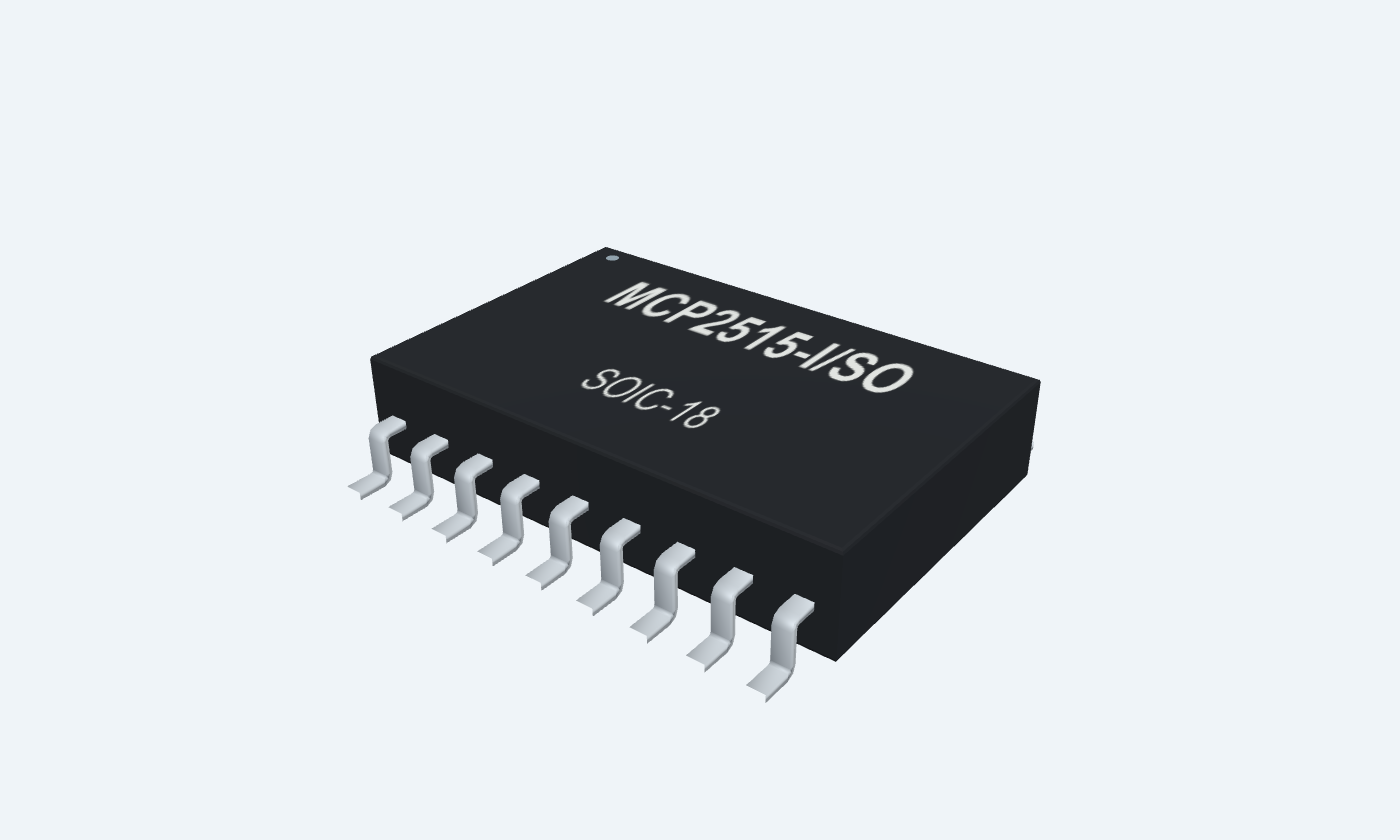

18Physical pins
MCP2515-I/PPDIP-18
Manufacturer-referencedMicrochip Technology
Pin diagram
Select a pin to explore its connection
Highlight
MCP2515PDIP-18Top view
MCP2515SOIC-18Top view
Click a lead or use the arrow keys. Top view
PIN 1 · CAN logic interface
Logic transmit outputTXCAN
Function
Sends the CAN protocol engine’s dominant/recessive logic to a transceiver.
How to connect
Connect to MCP2562 TXD pin 1.
Electrical note
This is not CANH or CANL; never connect directly to the cable.
PIN 2 · CAN logic interface
Logic receive inputRXCAN
Function
Receives the bus state from the external transceiver.
How to connect
Connect to MCP2562 RXD pin 4.
PIN 3 · Oscillator & clock
Clock or start-of-frame outputCLKOUT/SOF
Function
Outputs a divided oscillator clock or a selected start-of-frame indication.
How to connect
Leave open when unused.
Electrical note
After reset the enabled clock defaults to FOSC / 8.
PIN 4 · Reset & transmit requests
Request-to-send inputTX0RTS̅
Function
Active-LOW request for transmit buffer 0, or a general-purpose input according to TXRTSCTRL.
How to connect
Leave unconnected when unused; its internal pull-up holds it HIGH.
Electrical note
Approximately 100 kΩ internal pull-up to VDD.
PIN 5 · Reset & transmit requests
Request-to-send inputTX1RTS̅
Function
Active-LOW request for transmit buffer 1, or a general-purpose input according to TXRTSCTRL.
How to connect
Leave unconnected when unused; its internal pull-up holds it HIGH.
Electrical note
Approximately 100 kΩ internal pull-up to VDD.
PIN 6 · Reset & transmit requests
Request-to-send inputTX2RTS̅
Function
Active-LOW request for transmit buffer 2, or a general-purpose input according to TXRTSCTRL.
How to connect
Leave unconnected when unused; its internal pull-up holds it HIGH.
Electrical note
Approximately 100 kΩ internal pull-up to VDD.
PIN 7 · Oscillator & clock
Oscillator outputOSC2
Function
Feedback terminal for crystal/resonator operation.
How to connect
Leave open in the external-clock example.
PIN 8 · Oscillator & clock
Oscillator / clock inputOSC1
Function
Accepts the clock used for CAN bit timing and internal operation.
How to connect
Apply a 20 MHz, 0–5 V oscillator output with 45–55% duty cycle.
PIN 9 · Ground
Ground returnVSS
Function
Ground for logic, clock and I/O.
How to connect
Join the controller, oscillator and transceiver reference.
PIN 10 · Interrupts & flags
Receive-buffer 1 flagRX1BF̅
Function
Configurable buffer-full indication or general-purpose output.
How to connect
Leave open when using INT alone.
PIN 11 · Interrupts & flags
Receive-buffer 0 flagRX0BF̅
Function
Configurable buffer-full indication or general-purpose output.
How to connect
Leave open when using INT alone.
PIN 12 · Interrupts & flags
Active-LOW interruptINT̅
Function
Signals enabled interrupt conditions; software must inspect and service their flags.
How to connect
Connect to a compatible controller interrupt input.
PIN 13 · Host SPI
SPI clock inputSCK
Function
Clocks commands and register data; SPI modes 0 and 3 are supported.
How to connect
Connect controller SCK; use 1 MHz for the example.
PIN 14 · Host SPI
SPI data inputSI
Function
Receives instruction, address and data from the controller.
How to connect
Connect MOSI.
PIN 15 · Host SPI
SPI data outputSO
Function
Returns register and buffer data; high impedance when CS is HIGH.
How to connect
Connect MISO.
PIN 16 · Host SPI
Active-LOW chip selectCS̅
Function
LOW starts an SPI instruction; return HIGH before the next instruction.
How to connect
Connect a dedicated controller select and 10 kΩ pull-up to +5 V.
PIN 17 · Reset & transmit requests
Active-LOW resetRESET̅
Function
Initializes registers and enters Configuration mode.
How to connect
Use a 10 kΩ pull-up and controller reset output; hold LOW at least 2 µs.
Electrical note
Allow oscillator startup before SPI access.
PIN 18 · Supply
Positive supplyVDD
Function
Powers the CAN controller and its I/O.
How to connect
Use +5 V with 100 nF directly to VSS9.
Electrical note
Operating range 2.7–5.5 V; logic thresholds scale with supply.
Key specifications
The SPI host configures buffers, filters and timing. The CAN engine performs bus arbitration and error handling through TXCAN and RXCAN. A separate transceiver provides the electrical bus interface.
Classical CANUp to 1 Mbit/s
Operating supply2.7–5.5 V
Message buffers3 TX / 2 RX Six filters · two masks
Selected I-grade−40–85 °C
Package details
MCP2515-I/P · PDIP-18
| Property | Details |
|---|---|
| Manufacturer | Microchip Technology |
| Part number | MCP2515-I/P |
| Package | PDIP-18 |
| Connections | 18 pins |
| Mounting | Through-hole |
| Lead pitch | 2.54 mm |
| Package code | dip |
| Thermal reference | Board and package dependent; see manufacturer data |
Protocol and storage
Classical CAN 2.0B
Manufacturer specifications 7 parameters
Scroll sideways to see all columns.
| Parameter | Value | Conditions / notes |
|---|---|---|
| Bus rate | Up to 1 Mbit/s | Subject to oscillator and network timing |
| Identifiers | 11-bit standard / 29-bit extended | Data and remote frames |
| Data field | 0–8 bytes | No CAN FD or bit-rate switching |
| Transmit storage | Three prioritized buffers | Abort and one-shot options |
| Receive storage | Two buffers | Priority and optional rollover |
| Acceptance | Six filters and two masks | Configure before Normal mode |
| External line interface | Required CAN transceiver | TXCAN / RXCAN are logic signals |
No specifications match. Try a parameter name or a unit.
A controller and a transceiver solve different parts of the CAN interface.
Useful SPI instructions
Most significant bit first · separate CS cycle per command
Manufacturer specifications 8 parameters
Scroll sideways to see all columns.
| Parameter | Value | Conditions / notes |
|---|---|---|
| RESET | 0xC0 | Initialize and enter Configuration mode |
| READ | 0x03, address, dummy clocks | Consecutive register bytes may follow |
| WRITE | 0x02, address, data… | Sequential register write |
| BIT MODIFY | 0x05, address, mask, data | Only supported registers; mask 1 permits change |
| READ STATUS | 0xA0 | Frequently used RX/TX status |
| RX STATUS | 0xB0 | Received-frame type and matching filter |
| RTS buffer 0 | 0x81 | Request already-loaded TXB0 transmission |
| SPI timing | 10 MHz maximum; 50 ns CS setup/hold | Modes 0 and 3 |
No specifications match. Try a parameter name or a unit.
The controller expects an instruction immediately after CS falls. Raise CS before issuing another instruction.
Operating modes
Request via CANCTRL; confirm via CANSTAT
Manufacturer specifications 6 parameters
Scroll sideways to see all columns.
| Parameter | Value | Conditions / notes |
|---|---|---|
| Configuration | REQOP 100 | Required for bit timing, filters, masks and TXRTSCTRL |
| Normal | REQOP 000 | Transmit, receive and acknowledge CAN frames |
| Sleep | REQOP 001 | Oscillator stopped; wake-up conditions apply |
| Loopback | REQOP 010 | Internal communications test without bus transmission |
| Listen-only | REQOP 011 | Observe bus without transmitting or acknowledging |
| Mode confirmation | Read OPMOD bits | A request may wait for pending transmissions |
No specifications match. Try a parameter name or a unit.
Listen-only nodes do not supply the acknowledgment required for a transmitting node’s normal successful frame.
125 kbit/s configuration example
20 MHz external clock · single sample
Manufacturer specifications 8 parameters
Scroll sideways to see all columns.
| Parameter | Value | Conditions / notes |
|---|---|---|
| Oscillator period | 50 ns | 1 / 20 MHz |
| BRP register field | 4 | TQ = 2 × (BRP + 1) / FOSC |
| Time quantum | 500 ns | Prescaler division by 10 |
| Segments | Sync 1; Prop 2; PS1 7; PS2 6 | 16 TQ per bit |
| Sample point | (1 + 2 + 7) / 16 = 62.5% | At the end of Phase Segment 1 |
| Synchronization jump width | 1 TQ | Must not exceed PS2 |
| CNF1 / CNF2 / CNF3 | 0x04 / 0xB1 / 0x05 | BTLMODE=1, SAM=0; wake filter/SOF disabled |
| Result | 16 × 500 ns = 8 µs per bit | 125000 bits/s |
No specifications match. Try a parameter name or a unit.
This is the manufacturer’s illustrative timing split, not a universal network prescription. Review propagation, oscillator tolerance and the other nodes.
Supply, clock and logic
MCP2515-I/P and MCP2515-I/SO
Manufacturer specifications 10 parameters
Scroll sideways to see all columns.
| Parameter | Value | Conditions / notes |
|---|---|---|
| Operating supply / temperature | 2.7–5.5 V / −40 to +85°C | I grade |
| SPI input HIGH | ≥ 0.7 × VDD | SCK, SI and CS |
| SPI input LOW | ≤ 0.4 × VDD | SCK, SI and CS |
| RXCAN HIGH / LOW | ≥ 2.0 V / ≤ 0.15 × VDD | Different input thresholds from SPI |
| Reset HIGH / LOW | ≥ 0.85 × VDD / ≤ 0.15 × VDD | Schmitt reset input |
| External clock range | 1–25 MHz over 2.7–5.5 V | Up to 40 MHz at 4.5–5.5 V |
| Clock duty cycle | 45–55% | External clock input |
| Active current | 10 mA maximum | 5.5 V, oscillator25 MHz, SPI1 MHz, SO open |
| Sleep current, I grade | 5 µA maximum | Defined inputs and CS / TXnRTS HIGH |
| Hardware reset LOW | 2 µs minimum | Then allow 128 oscillator cycles for startup |
No specifications match. Try a parameter name or a unit.
At 5 V, a 3.3 V HIGH does not meet the SPI 0.7 VDD threshold. Use compatible levels or translation.
Controller-to-CAN connection
5 V logic · 20 MHz · 125 kbit/s
Manufacturer specifications 8 parameters
Scroll sideways to see all columns.
| Parameter | Value | Conditions / notes |
|---|---|---|
| Host SPI | SCK13, MOSI→SI14, SO15→MISO, CS16 | Start with mode0 at1 MHz |
| Host control | INT12→interrupt; RESET17→reset output | 10 kΩ pull-ups on CS and RESET |
| External oscillator | 20 MHz output→OSC1 pin8 | OSC2 pin7 open; oscillator bypass per its data |
| CAN controller/transceiver | TXCAN1→MCP2562 TXD1; RXD4→RXCAN2 | Logic connections, not bus pins |
| MCP2562 supplies | VDD3 and VIO5 to5 V; VSS2 GND | 100 nF local supply bypass; STBY8 LOW |
| Bus | MCP2562 CANH7 and CANL6 | Twisted pair; two120 Ω end terminators |
| Unused outputs | CLKOUT3, RX1BF10, RX0BF11 open | Unused TXnRTS inputs have internal pull-ups |
| Firmware | Reset, configure timing and filters, enter Normal mode | Another matching normal node must acknowledge |
No specifications match. Try a parameter name or a unit.
All ground references are common in this teaching circuit. Protection, isolation and cable length require a system-specific design.
Packages and stress limits
MCP2515-I/P · PDIP-18
Manufacturer specifications 6 parameters
Scroll sideways to see all columns.
| Parameter | Value | Conditions / notes |
|---|---|---|
| PDIP-18 P | 2.54 mm pitch; 7.62 mm rows | Narrow through-hole package |
| SOIC-18 SO | 1.27 mm pitch; 7.50 mm body width | Wide SOIC, not a narrow 3.9 mm body |
| Other packages | 20-lead TSSOP / QFN | Different contact maps; not interchangeable with18-pin views |
| Supply absolute maximum | 7.0 V | Normal operation ends at5.5 V |
| I/O absolute range | −0.6 to VDD + 1.0 V | Stress limits, not recommended input levels |
| Storage temperature | −65 to +150°C | Unpowered |
No specifications match. Try a parameter name or a unit.
Review the exact orderable and fabrication allowances before using the downloadable original footprints.
Connections by function
Select a pin for its function, connection guidance and electrical notes.
CAN logic interface2 pins
Oscillator & clock3 pins
Reset & transmit requests4 pins
Ground1 pin
Interrupts & flags3 pins
Host SPI4 pins
Supply1 pin
CAN logic interface2 pins
Oscillator & clock3 pins
Reset & transmit requests4 pins
Ground1 pin
Interrupts & flags3 pins
Host SPI4 pins
Supply1 pin
MCP2515 at a glance
Follow the labeled connections and functional stages
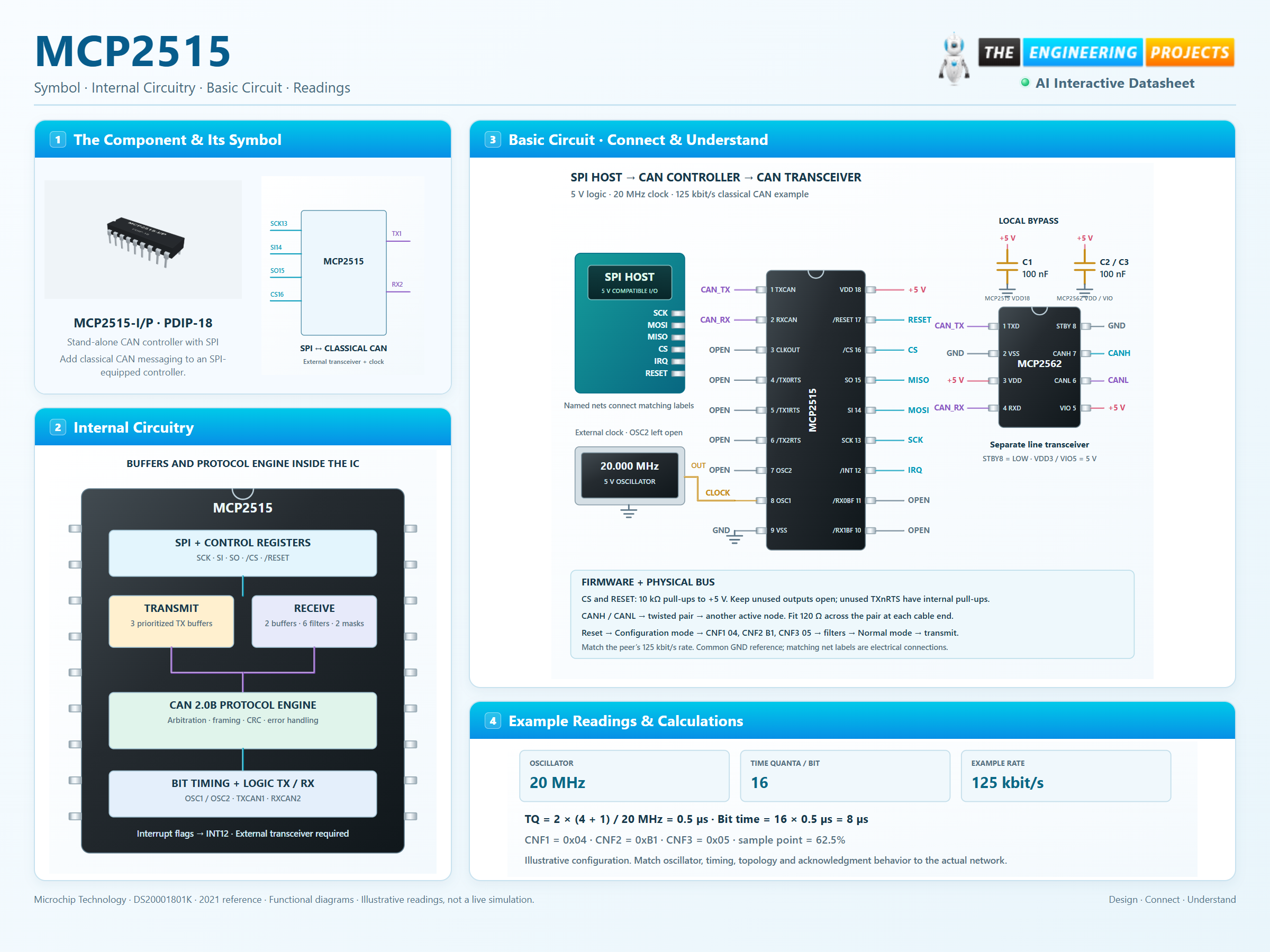
How it works
3 stages · Explore one step at a time
Configure through SPI
Reset, wait for oscillator startup and confirm Configuration mode before programming timing, masks and filters.
Buffer and arbitrate
Load an identifier and up to eight bytes into a transmit buffer, then request transmission. The engine handles arbitration and protocol errors.
Receive and service
Accepted frames enter receive buffers. Enabled flags assert INT; firmware reads the message and clears or services the cause.
Step 1 of 3
MCP2515 in a circuit
MCP2515 plus the separate MCP2562 bus transceiver.
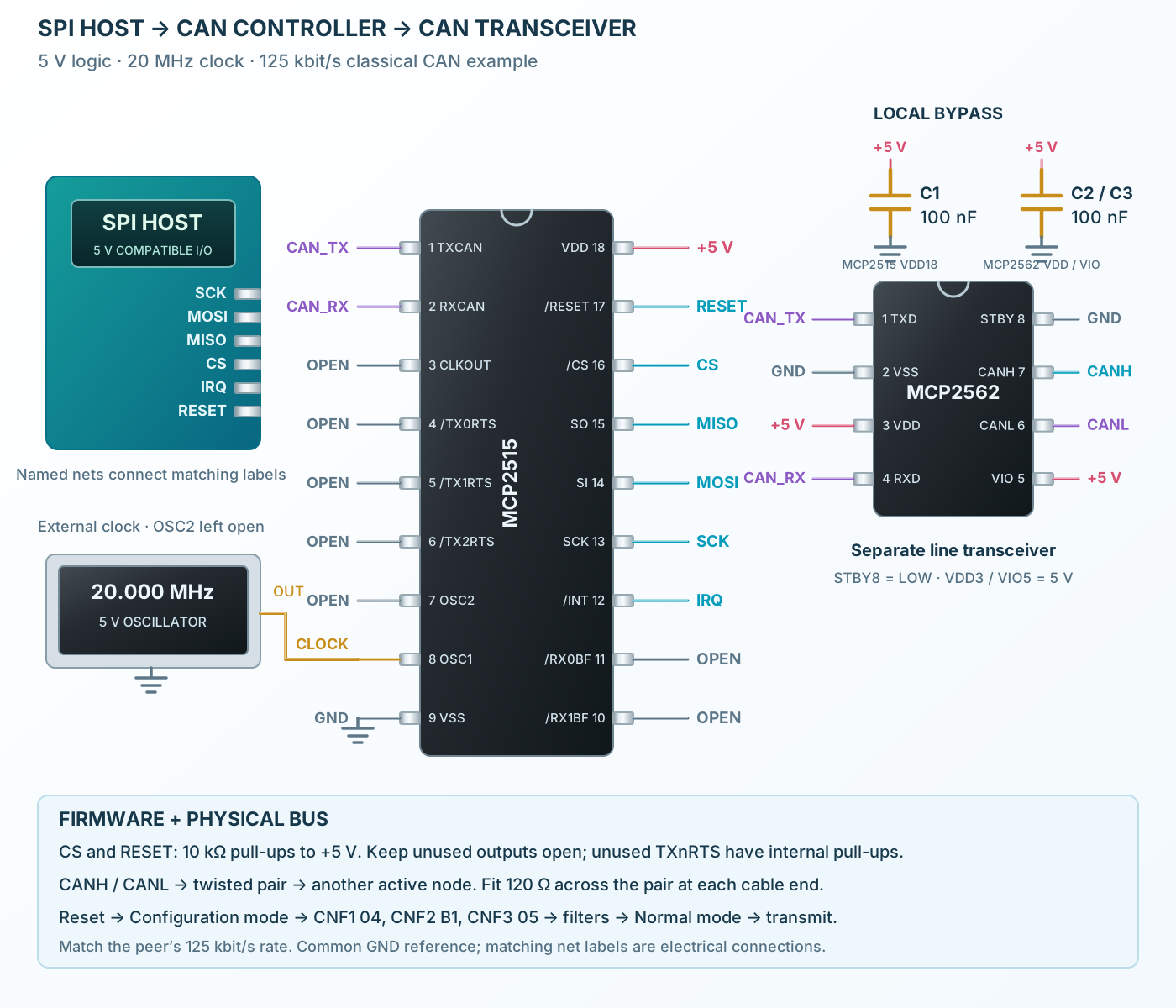
Connect it, step by step
Follow the component values and pin connections
Power and clock
Use compatible5 V logic, local bypassing and a valid20 MHz clock.
Configure the controller
Reset and program the125 kbit/s timing in Configuration mode before requesting Normal mode.
Connect the physical bus
The external transceiver drives CANH/CANL. Terminate both cable ends and provide a matching active peer.
Inside MCP2515
SPI control, buffers and a CAN engine inside the package.
Explore the circuit
Select a stage to see its role and connections
Host interface
SPI reads and writes configuration, message buffers and status.
Filter and buffer
Separate storage and acceptance logic reduce host involvement for unwanted traffic.
Time the bus
Oscillator-derived bit timing drives arbitration, framing, error detection and logic TX/RX.
Selected packagePDIP-18MCP2515-I/P
Physical connections18 pinsPackage-specific numbering
Reference collection8 tables53 parameters & pin functions
Pin reference
Signal names, electrical functions and connection guidance
Physical pin numbers18 pins
Scroll within the table to see all columns and rows.
| Pin | Signal | Type | Function & connection |
|---|---|---|---|
| TXCAN | Logic transmit output | Sends the CAN protocol engine’s dominant/recessive logic to a transceiver.Connection guidanceConnect to MCP2562 TXD pin 1. This is not CANH or CANL; never connect directly to the cable. | |
| RXCAN | Logic receive input | Receives the bus state from the external transceiver.Connection guidanceConnect to MCP2562 RXD pin 4. | |
| CLKOUT/SOF | Clock or start-of-frame output | Outputs a divided oscillator clock or a selected start-of-frame indication.Connection guidanceLeave open when unused. After reset the enabled clock defaults to FOSC / 8. | |
| TX0RTS̅ | Request-to-send input | Active-LOW request for transmit buffer 0, or a general-purpose input according to TXRTSCTRL.Connection guidanceLeave unconnected when unused; its internal pull-up holds it HIGH. Approximately 100 kΩ internal pull-up to VDD. | |
| TX1RTS̅ | Request-to-send input | Active-LOW request for transmit buffer 1, or a general-purpose input according to TXRTSCTRL.Connection guidanceLeave unconnected when unused; its internal pull-up holds it HIGH. Approximately 100 kΩ internal pull-up to VDD. | |
| TX2RTS̅ | Request-to-send input | Active-LOW request for transmit buffer 2, or a general-purpose input according to TXRTSCTRL.Connection guidanceLeave unconnected when unused; its internal pull-up holds it HIGH. Approximately 100 kΩ internal pull-up to VDD. | |
| OSC2 | Oscillator output | Feedback terminal for crystal/resonator operation.Connection guidanceLeave open in the external-clock example. | |
| OSC1 | Oscillator / clock input | Accepts the clock used for CAN bit timing and internal operation.Connection guidanceApply a 20 MHz, 0–5 V oscillator output with 45–55% duty cycle. | |
| VSS | Ground return | Ground for logic, clock and I/O.Connection guidanceJoin the controller, oscillator and transceiver reference. | |
| RX1BF̅ | Receive-buffer 1 flag | Configurable buffer-full indication or general-purpose output.Connection guidanceLeave open when using INT alone. | |
| RX0BF̅ | Receive-buffer 0 flag | Configurable buffer-full indication or general-purpose output.Connection guidanceLeave open when using INT alone. | |
| INT̅ | Active-LOW interrupt | Signals enabled interrupt conditions; software must inspect and service their flags.Connection guidanceConnect to a compatible controller interrupt input. | |
| SCK | SPI clock input | Clocks commands and register data; SPI modes 0 and 3 are supported.Connection guidanceConnect controller SCK; use 1 MHz for the example. | |
| SI | SPI data input | Receives instruction, address and data from the controller.Connection guidanceConnect MOSI. | |
| SO | SPI data output | Returns register and buffer data; high impedance when CS is HIGH.Connection guidanceConnect MISO. | |
| CS̅ | Active-LOW chip select | LOW starts an SPI instruction; return HIGH before the next instruction.Connection guidanceConnect a dedicated controller select and 10 kΩ pull-up to +5 V. | |
| RESET̅ | Active-LOW reset | Initializes registers and enters Configuration mode.Connection guidanceUse a 10 kΩ pull-up and controller reset output; hold LOW at least 2 µs. Allow oscillator startup before SPI access. | |
| VDD | Positive supply | Powers the CAN controller and its I/O.Connection guidanceUse +5 V with 100 nF directly to VSS9. Operating range 2.7–5.5 V; logic thresholds scale with supply. |
No pins match these filters. Try another signal name or reset the filters.
Protocol and storage
Classical CAN 2.0B
Manufacturer-referenced values7 parameters
Scroll within the table to see all columns and rows.
| Parameter | Value | Conditions / notes |
|---|---|---|
| Bus rate | Up to 1 Mbit/s | Subject to oscillator and network timing |
| Identifiers | 11-bit standard / 29-bit extended | Data and remote frames |
| Data field | 0–8 bytes | No CAN FD or bit-rate switching |
| Transmit storage | Three prioritized buffers | Abort and one-shot options |
| Receive storage | Two buffers | Priority and optional rollover |
| Acceptance | Six filters and two masks | Configure before Normal mode |
| External line interface | Required CAN transceiver | TXCAN / RXCAN are logic signals |
No specifications match. Try a parameter name or a unit.
A controller and a transceiver solve different parts of the CAN interface.
Useful SPI instructions
Most significant bit first · separate CS cycle per command
Manufacturer-referenced values8 parameters
Scroll within the table to see all columns and rows.
| Parameter | Value | Conditions / notes |
|---|---|---|
| RESET | 0xC0 | Initialize and enter Configuration mode |
| READ | 0x03, address, dummy clocks | Consecutive register bytes may follow |
| WRITE | 0x02, address, data… | Sequential register write |
| BIT MODIFY | 0x05, address, mask, data | Only supported registers; mask 1 permits change |
| READ STATUS | 0xA0 | Frequently used RX/TX status |
| RX STATUS | 0xB0 | Received-frame type and matching filter |
| RTS buffer 0 | 0x81 | Request already-loaded TXB0 transmission |
| SPI timing | 10 MHz maximum; 50 ns CS setup/hold | Modes 0 and 3 |
No specifications match. Try a parameter name or a unit.
The controller expects an instruction immediately after CS falls. Raise CS before issuing another instruction.
Operating modes
Request via CANCTRL; confirm via CANSTAT
Manufacturer-referenced values6 parameters
Scroll within the table to see all columns and rows.
| Parameter | Value | Conditions / notes |
|---|---|---|
| Configuration | REQOP 100 | Required for bit timing, filters, masks and TXRTSCTRL |
| Normal | REQOP 000 | Transmit, receive and acknowledge CAN frames |
| Sleep | REQOP 001 | Oscillator stopped; wake-up conditions apply |
| Loopback | REQOP 010 | Internal communications test without bus transmission |
| Listen-only | REQOP 011 | Observe bus without transmitting or acknowledging |
| Mode confirmation | Read OPMOD bits | A request may wait for pending transmissions |
No specifications match. Try a parameter name or a unit.
Listen-only nodes do not supply the acknowledgment required for a transmitting node’s normal successful frame.
125 kbit/s configuration example
20 MHz external clock · single sample
Manufacturer-referenced values8 parameters
Scroll within the table to see all columns and rows.
| Parameter | Value | Conditions / notes |
|---|---|---|
| Oscillator period | 50 ns | 1 / 20 MHz |
| BRP register field | 4 | TQ = 2 × (BRP + 1) / FOSC |
| Time quantum | 500 ns | Prescaler division by 10 |
| Segments | Sync 1; Prop 2; PS1 7; PS2 6 | 16 TQ per bit |
| Sample point | (1 + 2 + 7) / 16 = 62.5% | At the end of Phase Segment 1 |
| Synchronization jump width | 1 TQ | Must not exceed PS2 |
| CNF1 / CNF2 / CNF3 | 0x04 / 0xB1 / 0x05 | BTLMODE=1, SAM=0; wake filter/SOF disabled |
| Result | 16 × 500 ns = 8 µs per bit | 125000 bits/s |
No specifications match. Try a parameter name or a unit.
This is the manufacturer’s illustrative timing split, not a universal network prescription. Review propagation, oscillator tolerance and the other nodes.
Supply, clock and logic
MCP2515-I/P and MCP2515-I/SO
Manufacturer-referenced values10 parameters
Scroll within the table to see all columns and rows.
| Parameter | Value | Conditions / notes |
|---|---|---|
| Operating supply / temperature | 2.7–5.5 V / −40 to +85°C | I grade |
| SPI input HIGH | ≥ 0.7 × VDD | SCK, SI and CS |
| SPI input LOW | ≤ 0.4 × VDD | SCK, SI and CS |
| RXCAN HIGH / LOW | ≥ 2.0 V / ≤ 0.15 × VDD | Different input thresholds from SPI |
| Reset HIGH / LOW | ≥ 0.85 × VDD / ≤ 0.15 × VDD | Schmitt reset input |
| External clock range | 1–25 MHz over 2.7–5.5 V | Up to 40 MHz at 4.5–5.5 V |
| Clock duty cycle | 45–55% | External clock input |
| Active current | 10 mA maximum | 5.5 V, oscillator25 MHz, SPI1 MHz, SO open |
| Sleep current, I grade | 5 µA maximum | Defined inputs and CS / TXnRTS HIGH |
| Hardware reset LOW | 2 µs minimum | Then allow 128 oscillator cycles for startup |
No specifications match. Try a parameter name or a unit.
At 5 V, a 3.3 V HIGH does not meet the SPI 0.7 VDD threshold. Use compatible levels or translation.
Controller-to-CAN connection
5 V logic · 20 MHz · 125 kbit/s
Manufacturer-referenced values8 parameters
Scroll within the table to see all columns and rows.
| Parameter | Value | Conditions / notes |
|---|---|---|
| Host SPI | SCK13, MOSI→SI14, SO15→MISO, CS16 | Start with mode0 at1 MHz |
| Host control | INT12→interrupt; RESET17→reset output | 10 kΩ pull-ups on CS and RESET |
| External oscillator | 20 MHz output→OSC1 pin8 | OSC2 pin7 open; oscillator bypass per its data |
| CAN controller/transceiver | TXCAN1→MCP2562 TXD1; RXD4→RXCAN2 | Logic connections, not bus pins |
| MCP2562 supplies | VDD3 and VIO5 to5 V; VSS2 GND | 100 nF local supply bypass; STBY8 LOW |
| Bus | MCP2562 CANH7 and CANL6 | Twisted pair; two120 Ω end terminators |
| Unused outputs | CLKOUT3, RX1BF10, RX0BF11 open | Unused TXnRTS inputs have internal pull-ups |
| Firmware | Reset, configure timing and filters, enter Normal mode | Another matching normal node must acknowledge |
No specifications match. Try a parameter name or a unit.
All ground references are common in this teaching circuit. Protection, isolation and cable length require a system-specific design.
Packages and stress limits
MCP2515-I/P · PDIP-18
Manufacturer-referenced values6 parameters
Scroll within the table to see all columns and rows.
| Parameter | Value | Conditions / notes |
|---|---|---|
| PDIP-18 P | 2.54 mm pitch; 7.62 mm rows | Narrow through-hole package |
| SOIC-18 SO | 1.27 mm pitch; 7.50 mm body width | Wide SOIC, not a narrow 3.9 mm body |
| Other packages | 20-lead TSSOP / QFN | Different contact maps; not interchangeable with18-pin views |
| Supply absolute maximum | 7.0 V | Normal operation ends at5.5 V |
| I/O absolute range | −0.6 to VDD + 1.0 V | Stress limits, not recommended input levels |
| Storage temperature | −65 to +150°C | Unpowered |
No specifications match. Try a parameter name or a unit.
Review the exact orderable and fabrication allowances before using the downloadable original footprints.
No matching rowsTry a pin name, parameter, unit or test condition, or reset the filters.
SPI host expansion
Add classical CAN to a microcontroller that lacks an integrated CAN controller.
Manufacturer application guideNetwork diagnostics
Use listen-only mode and filtered reception to observe compatible CAN traffic.
Manufacturer application guideDistributed control
Exchange prioritized frames with suitable transceivers, cable topology and firmware.
Manufacturer application guideTake it into ProTech
Find MCP2515 in the Components Library to place its schematic symbol and connect its pins.
Reference page · circuit simulation model not yet availableOpen ProTech