Real View
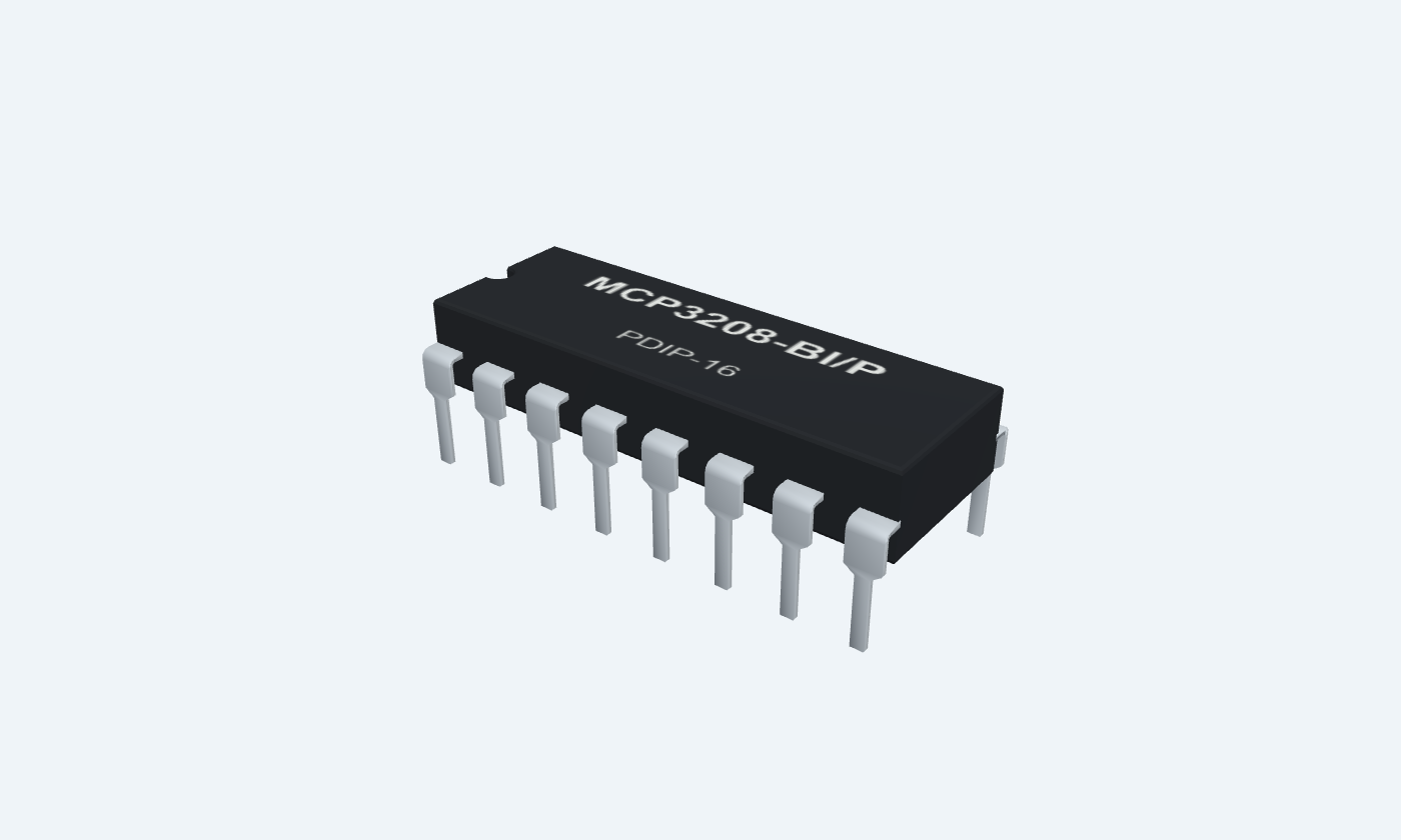
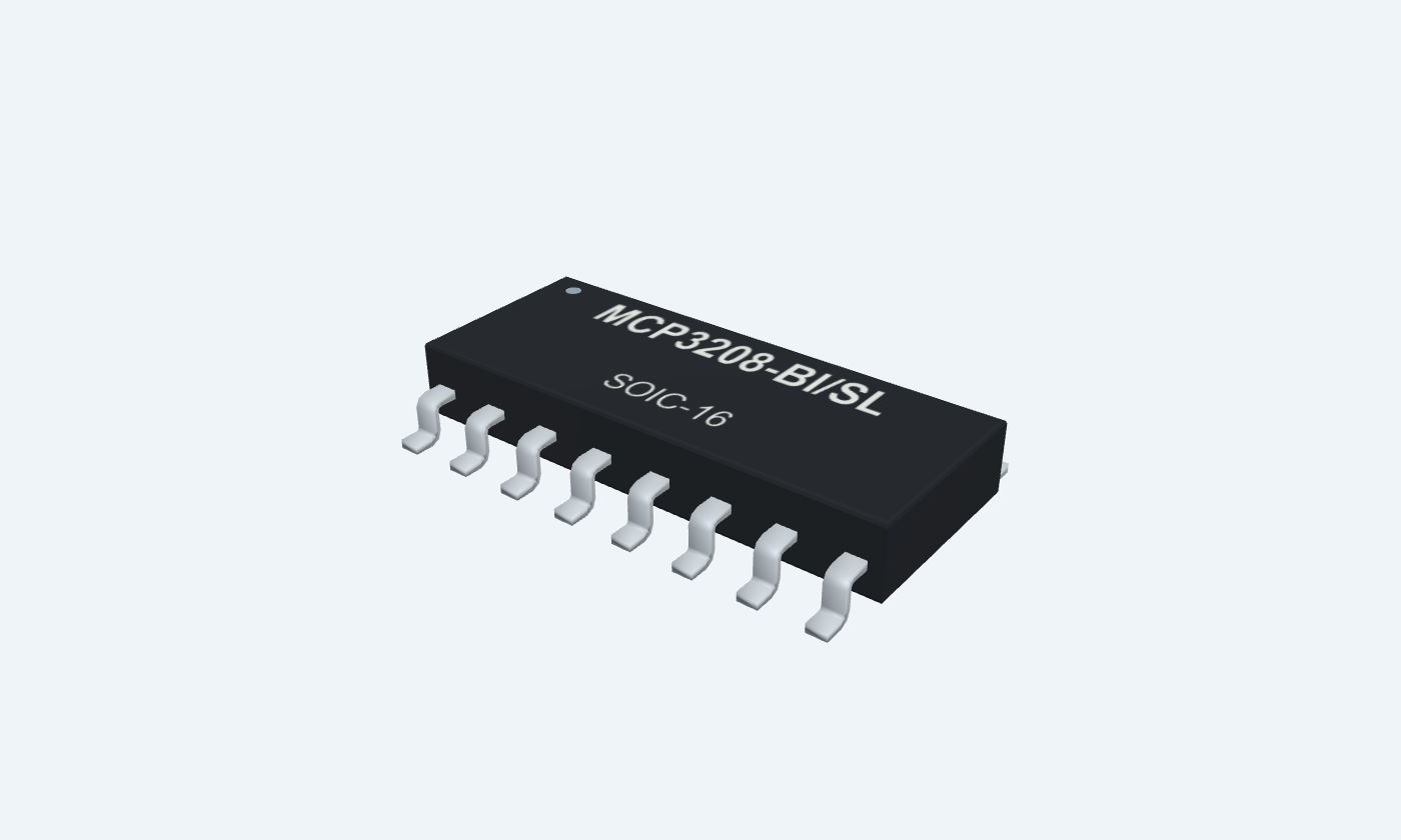
Eight analog inputs. Four thousand and ninety-six code levels.
MCP3208 is a 12-bit successive-approximation ADC with eight multiplexed analog inputs. Its SPI-compatible interface selects one channel and returns a straight-binary result from 0 to 4095. A sample-and-hold captures the selected voltage; channels are measured sequentially, not simultaneously. Single-ended inputs span ground to VREF. Four adjacent input pairs can also be used in pseudo-differential mode, with the negative input restricted to within 100 mV of ground. At a 3.3 V reference, one ideal code step is approximately 0.806 mV. The views show industrial B-grade PDIP-16 and SOIC-16 packages with ±1 LSB maximum integral nonlinearity. C-grade parts allow ±2 LSB. The example uses a compatible 3.3 V controller and a 1 MHz serial clock, with a quiet reference and local supply bypass.
Select a pin to explore its connection
Click a lead or use the arrow keys. Top view
Channel 0; selected by the three channel bits in the SPI command.
Connect a low-impedance signal within the selected reference range.
Single-ended: 0 to VREF. Pseudo-differential pairs are adjacent channels; IN− must stay within ±100 mV of ground.
Channel 1; selected by the three channel bits in the SPI command.
Connect a low-impedance signal within the selected reference range.
Single-ended: 0 to VREF. Pseudo-differential pairs are adjacent channels; IN− must stay within ±100 mV of ground.
Channel 2; selected by the three channel bits in the SPI command.
Connect a low-impedance signal within the selected reference range.
Single-ended: 0 to VREF. Pseudo-differential pairs are adjacent channels; IN− must stay within ±100 mV of ground.
Channel 3; selected by the three channel bits in the SPI command.
Connect a low-impedance signal within the selected reference range.
Single-ended: 0 to VREF. Pseudo-differential pairs are adjacent channels; IN− must stay within ±100 mV of ground.
Channel 4; selected by the three channel bits in the SPI command.
Connect a low-impedance signal within the selected reference range.
Single-ended: 0 to VREF. Pseudo-differential pairs are adjacent channels; IN− must stay within ±100 mV of ground.
Channel 5; selected by the three channel bits in the SPI command.
Connect a low-impedance signal within the selected reference range.
Single-ended: 0 to VREF. Pseudo-differential pairs are adjacent channels; IN− must stay within ±100 mV of ground.
Channel 6; selected by the three channel bits in the SPI command.
Connect a low-impedance signal within the selected reference range.
Single-ended: 0 to VREF. Pseudo-differential pairs are adjacent channels; IN− must stay within ±100 mV of ground.
Channel 7; selected by the three channel bits in the SPI command.
Connect a low-impedance signal within the selected reference range.
Single-ended: 0 to VREF. Pseudo-differential pairs are adjacent channels; IN− must stay within ±100 mV of ground.
Return for the SPI interface.
Join to the common ground plane.
LOW starts a serial transaction; HIGH ends it and enters standby.
Controller chip-select output with a defined HIGH idle state.
Return HIGH between conversions. A device powered up with CS LOW needs a HIGH-to-LOW sequence.
Receives the start bit, single/differential flag and channel address.
Controller MOSI; data is accepted on rising SCLK edges.
Returns a null bit followed by twelve conversion bits, most significant first.
Controller MISO.
Data changes on falling SCLK edges. DOUT is high impedance when CS is HIGH.
Clocks command entry, acquisition and successive approximation.
Controller SPI clock; use mode 0 or mode 3.
Meet the minimum effective conversion clock as well as the voltage-dependent maximum.
Reference return for the analog conversion.
Join to DGND using a quiet common ground layout.
Defines the input span and the ideal step size VREF / 4096.
A stable low-impedance reference, 0.25 V to VDD.
Reference quality and loading affect accuracy; do not leave this pin floating.
Powers the converter over 2.7–5.5 V.
Regulated supply with a nearby 1 µF bypass.
Match the SPI controller logic levels to this supply.
A multiplexer feeds the sample capacitor. The comparator, reference DAC and successive-approximation register resolve the input voltage before the serial port shifts out twelve bits.
MCP3208-BI/P · PDIP-16
| Property | Details |
|---|---|
| Manufacturer | Microchip Technology |
| Part number | MCP3208-BI/P |
| Package | PDIP-16 |
| Connections | 16 pins |
| Mounting | Through-hole |
| Lead pitch | 2.54 mm |
| Package code | PDIP-16 |
| Thermal reference | θJA 70°C/W · manufacturer package reference |
Industrial MCP3208-BI reference packages
Scroll sideways to see all columns.
| Parameter | Value | Conditions / notes |
|---|---|---|
| VDD | 2.7–5.5 V | Match controller I/O levels to this supply |
| VREF | 0.25 V to VDD | Stable, low-impedance reference; low values affect linearity |
| Single-ended input | 0 to VREF | Relative to AGND |
| Pseudo-differential IN− | −100 to +100 mV | Near ground, not arbitrary common-mode voltage |
| Pseudo-differential IN+ | IN− to IN− + VREF | Also observe physical pin voltage limits |
| Selected ambient range | −40 to +85°C | Industrial I grade |
| Conversions | One channel at a time | Not simultaneous sampling |
No specifications match. Try a parameter name or a unit.
Operating limits are distinct from absolute maximum stress ratings.
Manufacturer electrical conditions: VDD=VREF=5 V
Scroll sideways to see all columns.
| Parameter | Value | Conditions / notes |
|---|---|---|
| Resolution | 12 bits | 4096 codes; 0…4095 |
| Ideal LSB at 3.3 V | 0.8056640625 mV | VREF / 4096 |
| B-grade INL | ±1 LSB maximum | ±0.75 LSB typical |
| C-grade INL | ±2 LSB maximum | ±1 LSB typical; not the selected B-grade |
| DNL | ±1 LSB maximum | ±0.5 LSB typical; no missing codes |
| Offset error | ±3 LSB maximum | ±1.25 LSB typical |
| Gain error | ±5 LSB maximum | ±1.25 LSB typical |
| SINAD | 72 dB typical | 1 kHz, 0.1–4.9 V input |
No specifications match. Try a parameter name or a unit.
The calculator excludes these errors and external reference uncertainty.
Supply-dependent rate and loading
Scroll sideways to see all columns.
| Parameter | Value | Conditions / notes |
|---|---|---|
| Acquisition interval | 1.5 clock periods | Source must settle to twelve-bit accuracy |
| Conversion interval | 12 clocks | Additional command/framing clocks are required |
| Maximum rate at 5 V | 100 ksps | 2 MHz serial clock, 20-clock conversion framing |
| Maximum rate at 2.7 V | 50 ksps | 1 MHz serial clock |
| CS HIGH interval | 500 ns minimum | Between conversions |
| CS LOW to first rising clock | 100 ns minimum | Serial setup |
| DIN setup / hold | 50 ns / 50 ns minimum | Around rising clock edge |
| Output valid after falling clock | 200 ns maximum | Manufacturer timing test |
| Minimum effective clock | 10 kHz | Finish the conversion within 1.2 ms after acquisition |
No specifications match. Try a parameter name or a unit.
Three-byte transfers add clocks and CS overhead, so a 1 MHz example remains below 41.7 k conversions per second.
MCP3208 mode 0 or mode 3
Scroll sideways to see all columns.
| Parameter | Value | Conditions / notes |
|---|---|---|
| TX0, single-ended | 0x06 | (channel >> 2) | Five leading zeros, START, SGL and D2 |
| TX1 | (channel & 3) << 6 | D1 and D0, followed by zeros |
| TX2 | 0x00 | Clocks out the remaining result |
| Pseudo-differential TX0 | 0x04 | (channel >> 2) | Clears SGL; adjacent channel is IN− |
| RX0 | Discard | No result bits |
| RX1 | Keep low nibble | B11…B8; discard upper four bits |
| RX2 | Keep all eight bits | B7…B0 |
| Result | ((RX1 & 0x0F) << 8) | RX2 | RX indices are zero-based |
| CH0 example | 06 00 00 → XX X8 00 | Ideal half-scale result 2048 |
No specifications match. Try a parameter name or a unit.
Raise CS between transfers. DOUT becomes high impedance while CS is HIGH.
Use specified test conditions
Scroll sideways to see all columns.
| Parameter | Value | Conditions / notes |
|---|---|---|
| Digital input HIGH / LOW | ≥0.7×VDD / ≤0.3×VDD | Do not assume 3.3 V HIGH is valid at a 5 V ADC |
| Active supply current at 5 V | 320 µA typical; 400 µA maximum | VDD=VREF=5 V, DOUT unloaded |
| Active current at 2.7 V | 225 µA typical | VDD=VREF=2.7 V |
| Standby current | 0.5 µA typical; 2 µA maximum | CS=VDD=5 V |
| Reference current while converting | 100 µA typical; 150 µA maximum | Reference must handle dynamic load |
| Analog leakage | ±1 µA maximum | 0.001 µA typical |
| Sampling capacitor / switch | 20 pF / 1 kΩ typical | Source resistance adds acquisition error |
| Package thermal reference | θJA 70°C/W · manufacturer package reference | Board construction changes actual thermal performance |
No specifications match. Try a parameter name or a unit.
Use low-impedance analog sources and separate quiet analog returns from clock current paths.
Color-coded SPI circuit and ideal readings
Scroll sideways to see all columns.
| Parameter | Value | Conditions / notes |
|---|---|---|
| VDD16 and VREF15 | Regulated 3.3 V | Both connected, reference not floating |
| Grounds | AGND14 and DGND9 | Common ground, quiet layout |
| Supply bypass | 1 µF close to VDD | Manufacturer application guidance |
| Signal input | 1.650 V on CH0 pin1 | Low-impedance source; unused inputs grounded in example |
| Serial connection | CS10, DIN11, DOUT12, CLK13 | CS, MOSI, MISO and SCLK |
| Serial clock | 1 MHz, mode 0 | 24 clocks per example transfer, plus CS HIGH interval |
| Ideal output | 2048 · 0x800 | Nominal half scale |
| Decode voltage | code × VREF / 4096 | A nominal reconstruction, not sub-LSB accuracy |
No specifications match. Try a parameter name or a unit.
The sample is analog; fast or high-impedance sensors may require buffering and filtering.
Select a pin for its function, connection guidance and electrical notes.
Follow the labeled connections and functional stages
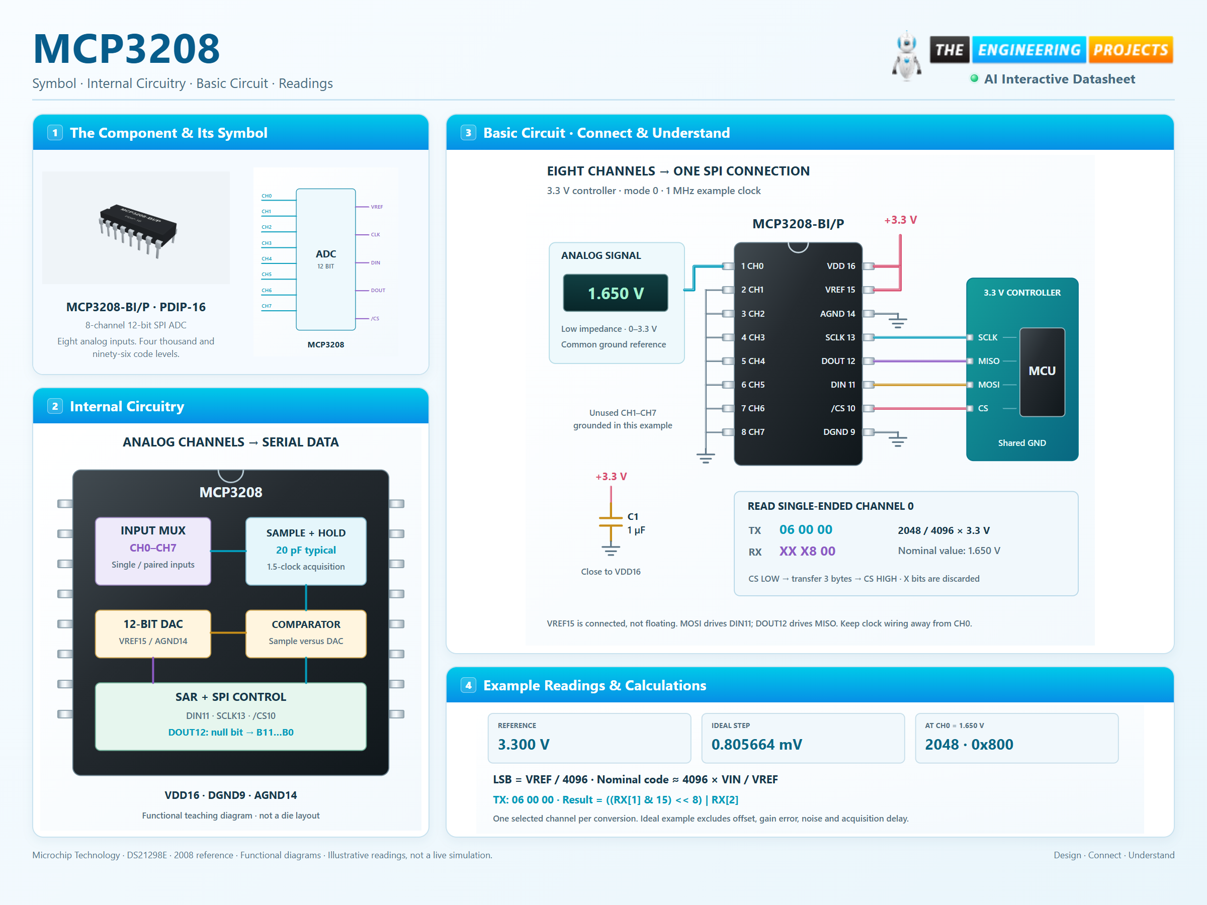
3 stages · Explore one step at a time
CS LOW starts the transaction. Send START, SGL/DIFF and channel bits D2–D0.
The source charges the sample capacitor over 1.5 clocks. Twelve successive approximation steps resolve the held voltage.
Discard the null/framing bits, combine the last four bits of RX1 with RX2, then raise CS.
Explore 12-bit conversion and single-ended or pseudo-differential inputs.
Channel selection is part of every conversion command. Differential results remain unsigned; a negative difference clips to zero.
06 00 00Three transmit bytes · hexadecimalXX X8 00X = discard · retain 12 result bitsCS pin 10 stays LOW for the transaction. Use SCLK pin 13, mode 0 or 3. Read ((RX[1] & 15) << 8) | RX[2], then raise CS. Ideal MCP3208 code and SPI framing explorer. Rounds to the nearest nominal code and clamps to 0–4095; excludes noise, acquisition delay and offset/gain error. IN− must stay within ±100 mV of ground.
A physical MCP3208 and a 3.3 V controller share a quiet supply.
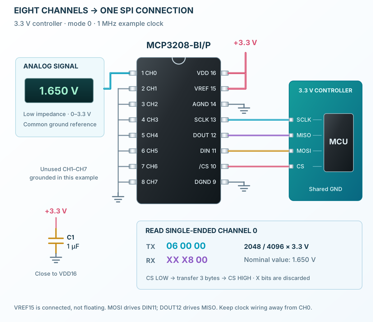
Follow the component values and pin connections
Connect both VDD and VREF to 3.3 V, join the grounds and place the 1 µF bypass nearby.
Use MOSI→DIN, DOUT→MISO, SCLK→SCLK and a separate chip-select line.
Send 06 00 00 to select single-ended CH0. Combine the twelve returned data bits; raise CS between measurements.
Eight inputs share a sample-and-hold and twelve-bit SAR core.
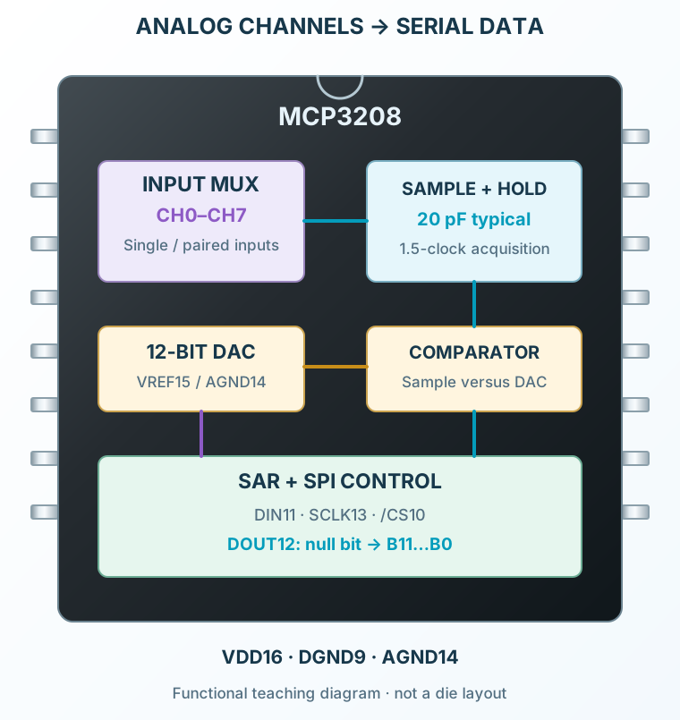
Select a stage to see its role and connections
The command selects a single input or adjacent pseudo-differential pair.
A sample capacitor stores the voltage while the SAR tests successive DAC levels.
The result is shifted out MSB first; CS HIGH releases DOUT and ends the conversion.
Signal names, electrical functions and connection guidance
Scroll within the table to see all columns and rows.
| Pin | Signal | Type | Function & connection |
|---|---|---|---|
| CH0 | Multiplexed analog input | Channel 0; selected by the three channel bits in the SPI command.Connection guidanceConnect a low-impedance signal within the selected reference range. Single-ended: 0 to VREF. Pseudo-differential pairs are adjacent channels; IN− must stay within ±100 mV of ground. | |
| CH1 | Multiplexed analog input | Channel 1; selected by the three channel bits in the SPI command.Connection guidanceConnect a low-impedance signal within the selected reference range. Single-ended: 0 to VREF. Pseudo-differential pairs are adjacent channels; IN− must stay within ±100 mV of ground. | |
| CH2 | Multiplexed analog input | Channel 2; selected by the three channel bits in the SPI command.Connection guidanceConnect a low-impedance signal within the selected reference range. Single-ended: 0 to VREF. Pseudo-differential pairs are adjacent channels; IN− must stay within ±100 mV of ground. | |
| CH3 | Multiplexed analog input | Channel 3; selected by the three channel bits in the SPI command.Connection guidanceConnect a low-impedance signal within the selected reference range. Single-ended: 0 to VREF. Pseudo-differential pairs are adjacent channels; IN− must stay within ±100 mV of ground. | |
| CH4 | Multiplexed analog input | Channel 4; selected by the three channel bits in the SPI command.Connection guidanceConnect a low-impedance signal within the selected reference range. Single-ended: 0 to VREF. Pseudo-differential pairs are adjacent channels; IN− must stay within ±100 mV of ground. | |
| CH5 | Multiplexed analog input | Channel 5; selected by the three channel bits in the SPI command.Connection guidanceConnect a low-impedance signal within the selected reference range. Single-ended: 0 to VREF. Pseudo-differential pairs are adjacent channels; IN− must stay within ±100 mV of ground. | |
| CH6 | Multiplexed analog input | Channel 6; selected by the three channel bits in the SPI command.Connection guidanceConnect a low-impedance signal within the selected reference range. Single-ended: 0 to VREF. Pseudo-differential pairs are adjacent channels; IN− must stay within ±100 mV of ground. | |
| CH7 | Multiplexed analog input | Channel 7; selected by the three channel bits in the SPI command.Connection guidanceConnect a low-impedance signal within the selected reference range. Single-ended: 0 to VREF. Pseudo-differential pairs are adjacent channels; IN− must stay within ±100 mV of ground. | |
| DGND | Digital ground | Return for the SPI interface.Connection guidanceJoin to the common ground plane. | |
| /CS/SHDN | Active-LOW chip select | LOW starts a serial transaction; HIGH ends it and enters standby.Connection guidanceController chip-select output with a defined HIGH idle state. Return HIGH between conversions. A device powered up with CS LOW needs a HIGH-to-LOW sequence. | |
| DIN | Serial command input | Receives the start bit, single/differential flag and channel address.Connection guidanceController MOSI; data is accepted on rising SCLK edges. | |
| DOUT | Serial conversion output | Returns a null bit followed by twelve conversion bits, most significant first.Connection guidanceController MISO. Data changes on falling SCLK edges. DOUT is high impedance when CS is HIGH. | |
| SCLK | Serial clock | Clocks command entry, acquisition and successive approximation.Connection guidanceController SPI clock; use mode 0 or mode 3. Meet the minimum effective conversion clock as well as the voltage-dependent maximum. | |
| AGND | Analog ground | Reference return for the analog conversion.Connection guidanceJoin to DGND using a quiet common ground layout. | |
| VREF | Conversion reference | Defines the input span and the ideal step size VREF / 4096.Connection guidanceA stable low-impedance reference, 0.25 V to VDD. Reference quality and loading affect accuracy; do not leave this pin floating. | |
| VDD | Supply | Powers the converter over 2.7–5.5 V.Connection guidanceRegulated supply with a nearby 1 µF bypass. Match the SPI controller logic levels to this supply. |
No pins match these filters. Try another signal name or reset the filters.
Industrial MCP3208-BI reference packages
Scroll within the table to see all columns and rows.
| Parameter | Value | Conditions / notes |
|---|---|---|
| VDD | 2.7–5.5 V | Match controller I/O levels to this supply |
| VREF | 0.25 V to VDD | Stable, low-impedance reference; low values affect linearity |
| Single-ended input | 0 to VREF | Relative to AGND |
| Pseudo-differential IN− | −100 to +100 mV | Near ground, not arbitrary common-mode voltage |
| Pseudo-differential IN+ | IN− to IN− + VREF | Also observe physical pin voltage limits |
| Selected ambient range | −40 to +85°C | Industrial I grade |
| Conversions | One channel at a time | Not simultaneous sampling |
No specifications match. Try a parameter name or a unit.
Operating limits are distinct from absolute maximum stress ratings.
Manufacturer electrical conditions: VDD=VREF=5 V
Scroll within the table to see all columns and rows.
| Parameter | Value | Conditions / notes |
|---|---|---|
| Resolution | 12 bits | 4096 codes; 0…4095 |
| Ideal LSB at 3.3 V | 0.8056640625 mV | VREF / 4096 |
| B-grade INL | ±1 LSB maximum | ±0.75 LSB typical |
| C-grade INL | ±2 LSB maximum | ±1 LSB typical; not the selected B-grade |
| DNL | ±1 LSB maximum | ±0.5 LSB typical; no missing codes |
| Offset error | ±3 LSB maximum | ±1.25 LSB typical |
| Gain error | ±5 LSB maximum | ±1.25 LSB typical |
| SINAD | 72 dB typical | 1 kHz, 0.1–4.9 V input |
No specifications match. Try a parameter name or a unit.
The calculator excludes these errors and external reference uncertainty.
Supply-dependent rate and loading
Scroll within the table to see all columns and rows.
| Parameter | Value | Conditions / notes |
|---|---|---|
| Acquisition interval | 1.5 clock periods | Source must settle to twelve-bit accuracy |
| Conversion interval | 12 clocks | Additional command/framing clocks are required |
| Maximum rate at 5 V | 100 ksps | 2 MHz serial clock, 20-clock conversion framing |
| Maximum rate at 2.7 V | 50 ksps | 1 MHz serial clock |
| CS HIGH interval | 500 ns minimum | Between conversions |
| CS LOW to first rising clock | 100 ns minimum | Serial setup |
| DIN setup / hold | 50 ns / 50 ns minimum | Around rising clock edge |
| Output valid after falling clock | 200 ns maximum | Manufacturer timing test |
| Minimum effective clock | 10 kHz | Finish the conversion within 1.2 ms after acquisition |
No specifications match. Try a parameter name or a unit.
Three-byte transfers add clocks and CS overhead, so a 1 MHz example remains below 41.7 k conversions per second.
MCP3208 mode 0 or mode 3
Scroll within the table to see all columns and rows.
| Parameter | Value | Conditions / notes |
|---|---|---|
| TX0, single-ended | 0x06 | (channel >> 2) | Five leading zeros, START, SGL and D2 |
| TX1 | (channel & 3) << 6 | D1 and D0, followed by zeros |
| TX2 | 0x00 | Clocks out the remaining result |
| Pseudo-differential TX0 | 0x04 | (channel >> 2) | Clears SGL; adjacent channel is IN− |
| RX0 | Discard | No result bits |
| RX1 | Keep low nibble | B11…B8; discard upper four bits |
| RX2 | Keep all eight bits | B7…B0 |
| Result | ((RX1 & 0x0F) << 8) | RX2 | RX indices are zero-based |
| CH0 example | 06 00 00 → XX X8 00 | Ideal half-scale result 2048 |
No specifications match. Try a parameter name or a unit.
Raise CS between transfers. DOUT becomes high impedance while CS is HIGH.
Use specified test conditions
Scroll within the table to see all columns and rows.
| Parameter | Value | Conditions / notes |
|---|---|---|
| Digital input HIGH / LOW | ≥0.7×VDD / ≤0.3×VDD | Do not assume 3.3 V HIGH is valid at a 5 V ADC |
| Active supply current at 5 V | 320 µA typical; 400 µA maximum | VDD=VREF=5 V, DOUT unloaded |
| Active current at 2.7 V | 225 µA typical | VDD=VREF=2.7 V |
| Standby current | 0.5 µA typical; 2 µA maximum | CS=VDD=5 V |
| Reference current while converting | 100 µA typical; 150 µA maximum | Reference must handle dynamic load |
| Analog leakage | ±1 µA maximum | 0.001 µA typical |
| Sampling capacitor / switch | 20 pF / 1 kΩ typical | Source resistance adds acquisition error |
| Package thermal reference | θJA 70°C/W · manufacturer package reference | Board construction changes actual thermal performance |
No specifications match. Try a parameter name or a unit.
Use low-impedance analog sources and separate quiet analog returns from clock current paths.
Color-coded SPI circuit and ideal readings
Scroll within the table to see all columns and rows.
| Parameter | Value | Conditions / notes |
|---|---|---|
| VDD16 and VREF15 | Regulated 3.3 V | Both connected, reference not floating |
| Grounds | AGND14 and DGND9 | Common ground, quiet layout |
| Supply bypass | 1 µF close to VDD | Manufacturer application guidance |
| Signal input | 1.650 V on CH0 pin1 | Low-impedance source; unused inputs grounded in example |
| Serial connection | CS10, DIN11, DOUT12, CLK13 | CS, MOSI, MISO and SCLK |
| Serial clock | 1 MHz, mode 0 | 24 clocks per example transfer, plus CS HIGH interval |
| Ideal output | 2048 · 0x800 | Nominal half scale |
| Decode voltage | code × VREF / 4096 | A nominal reconstruction, not sub-LSB accuracy |
No specifications match. Try a parameter name or a unit.
The sample is analog; fast or high-impedance sensors may require buffering and filtering.
No matching rowsTry a pin name, parameter, unit or test condition, or reset the filters.
Acquire eight conditioned voltages with a shared reference and SPI link.
Manufacturer application guideAdd external analog channels to a controller or processor.
Manufacturer application guideReturn CS HIGH between measurements to reduce standby consumption.
Manufacturer application guideFind MCP3208 in the Components Library to place its schematic symbol and connect its pins.
Reference page · circuit simulation model not yet availableOpen ProTech