MCP472512-bit I²C DAC with EEPROM
Turn a digital setpoint into a steady analog voltage.
MCP4725 is a single-channel 12-bit digital-to-analog converter with a buffered voltage output and nonvolatile EEPROM. A controller sends a code over I²C, and the IC produces the corresponding analog level. It uses its supply voltage as the DAC reference, so a clean and accurate supply is part of the measurement chain. The output code ranges from zero to 4095. Ideally, VOUT equals VDD multiplied by the code and divided by 4096; the highest code is one step below the supply. With 3.3 V at VDD, code 2048 produces 1.650 V before real offset, gain and loading errors. Ordinary DAC writes change the output without wearing the EEPROM. A separate command stores the chosen startup value and power-down state for the next power cycle. The example uses the MCP4725A0T-E/CH six-pin package at address 0x60 and updates only the volatile DAC register.
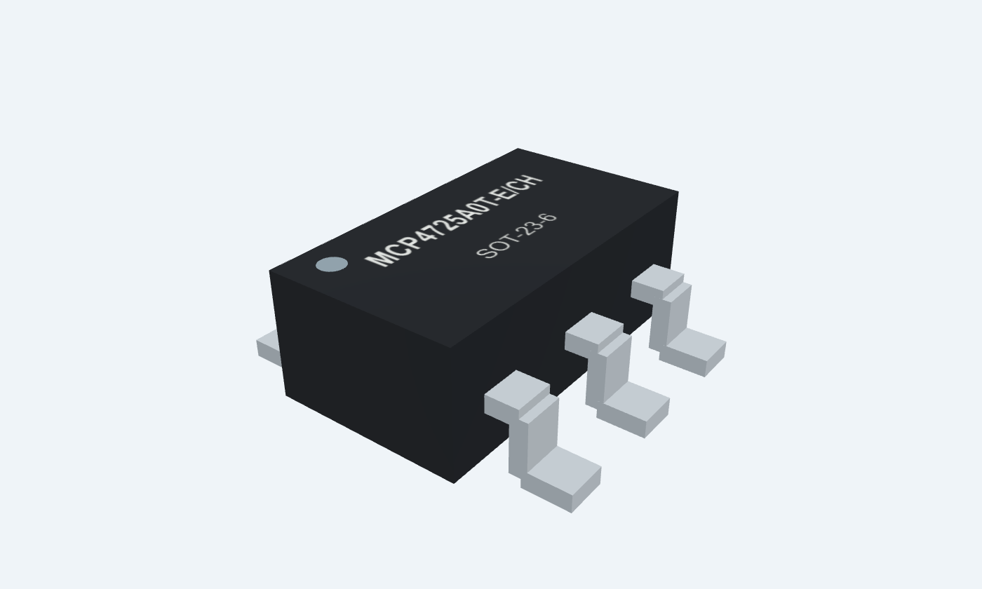

6Physical pins
MCP4725A0T-E/CHSOT-23-6
Manufacturer-referencedMicrochip Technology
Pin diagram
Select a pin to explore its connection
Highlight
MCP4725SOT-23-6Top view
Click a lead or use the arrow keys. Top view
PIN 1 · Analog voltage output
Buffered analog outputVOUT
Function
Outputs the voltage selected by the 12-bit DAC code.
How to connect
Connect a high-impedance meter or suitable analog load.
Electrical note
The ideal scale uses VDD / 4096. Loading, offset, gain error and output headroom affect real results.
PIN 2 · Ground
GroundVSS
Function
Supply and analog-output reference.
How to connect
Join controller ground and measurement return.
PIN 3 · Supply
Supply and DAC referenceVDD
Function
The supply also determines the output conversion scale.
How to connect
Use a clean 3.3 V rail, with 100 nF and local bulk bypass to VSS.
Electrical note
Supply noise and supply error directly affect the analog output.
PIN 4 · I²C interface
I²C serial dataSDA
Function
Bidirectional open-drain data connection.
How to connect
Connect to controller SDA and a pull-up to VDD.
PIN 5 · I²C interface
I²C serial clockSCL
Function
Clock connection for the I²C controller.
How to connect
Connect to controller SCL and a pull-up to VDD.
PIN 6 · Address selection
Address selectionA0
Function
Sets the least-significant address bit; two upper address bits are factory options.
How to connect
Tie LOW for 0x60 on the selected A0 orderable, or HIGH for 0x61.
Electrical note
Do not confuse the external A0 pin with the A0 suffix in the ordering code.
Key specifications
The I²C register selects a resistive-string DAC level. A buffer drives VOUT; EEPROM optionally remembers a startup setting. VDD is both power and reference.
Resolution12 bits · 4096 codes
Supply / reference2.7–5.5 V
Typical settling6 µs · specified step/load
Operating ambient−40–125 °C
Package details
MCP4725A0T-E/CH · SOT-23-6
| Property | Details |
|---|---|
| Manufacturer | Microchip Technology |
| Part number | MCP4725A0T-E/CH |
| Package | SOT-23-6 |
| Connections | 6 pins |
| Mounting | SMD |
| Lead pitch | 0.95 mm |
| Package code | smd |
| Thermal reference | θJA 190.5°C/W · manufacturer reference |
Operating and interface limits
Extended-temperature grade
Manufacturer specifications 7 parameters
Scroll sideways to see all columns.
| Parameter | Value | Conditions / notes |
|---|---|---|
| Supply / DAC reference | 2.7–5.5 V | Same VDD pin for power and conversion scale |
| Operating ambient | −40 to +125°C | Selected E grade |
| Code range | 0–4095 | Unsigned 12-bit code |
| I²C modes | 100 kHz, 400 kHz, 3.4 MHz | High-speed mode requires its specified protocol |
| SDA/SCL input HIGH / LOW | ≥ 0.7 VDD / ≤ 0.3 VDD | Use compatible logic levels |
| A0 input HIGH / LOW | ≥ 0.8 VDD / ≤ 0.2 VDD | Different from SDA/SCL thresholds |
| Supply current | 210 µA typical / 400 µA maximum | Code zero; digital inputs grounded; VOUT unloaded |
No specifications match. Try a parameter name or a unit.
Absolute maximum supply is a stress rating and must not replace the recommended operating range.
Ideal transfer at 3.3 V
VOUT = VDD × code / 4096
Manufacturer specifications 6 parameters
Scroll sideways to see all columns.
| Parameter | Value | Conditions / notes |
|---|---|---|
| Code 0 / 0x000 | 0 V ideal | Real zero-scale offset remains |
| Code 1 / 0x001 | 0.000805664 V | One ideal LSB |
| Code 1024 / 0x400 | 0.825 V | Quarter-scale |
| Code 2048 / 0x800 | 1.650 V | Midscale example |
| Code 3072 / 0xC00 | 2.475 V | Three-quarter scale |
| Code 4095 / 0xFFF | 3.299194 V | One ideal LSB below VDD |
No specifications match. Try a parameter name or a unit.
A rail-to-rail amplifier is still affected by load and headroom near either supply.
I²C command examples
Selected A0 factory option; external A0 LOW
Manufacturer specifications 7 parameters
Scroll sideways to see all columns.
| Parameter | Value | Conditions / notes |
|---|---|---|
| Seven-bit address | 0x60 | 0xC0 write / 0xC1 read are address bytes, not seven-bit addresses |
| External A0 HIGH | 0x61 | Other factory options provide the remaining address pairs |
| Fast write, midpoint | Data bytes 0x08 0x00 | PD=00; code=0x800; EEPROM unchanged |
| DAC-register write | Data bytes 0x40 0x80 0x00 | Same code via three-byte command format |
| DAC + EEPROM write | Data bytes 0x60 0x80 0x00 | Intentional persistent startup setting |
| Read sequence | Five data bytes after the address | Current status, DAC code and EEPROM content |
| RDY/BSY status | 1 ready; 0 EEPROM write in progress | Returned status bit; no separate ready pin |
No specifications match. Try a parameter name or a unit.
Do not send new write commands during an EEPROM write. Check the returned ready status first.
EEPROM and power modes
Preserve endurance by choosing the correct command
Manufacturer specifications 6 parameters
Scroll sideways to see all columns.
| Parameter | Value | Conditions / notes |
|---|---|---|
| EEPROM write duration | 25 ms typical / 50 ms maximum | Poll RDY/BSY rather than assuming immediate completion |
| EEPROM endurance | 1 million cycles minimum at +25°C | Design-assured parameter, not 100% tested |
| Data retention | 200 years typical at +25°C | Temperature and conditions matter |
| Startup | Loads stored code and mode | Observe the specified VDD ramp conditions |
| PD 00 | Normal output buffer | DAC output enabled |
| PD 01 / 10 / 11 | 1 kΩ / 100 kΩ / 500 kΩ to ground | Typical output resistance with amplifier powered down |
No specifications match. Try a parameter name or a unit.
Nonvolatile memory is for remembered settings, not continuous waveform updates.
Accuracy and dynamic behavior
Datasheet test conditions apply
Manufacturer specifications 6 parameters
Scroll sideways to see all columns.
| Parameter | Value | Conditions / notes |
|---|---|---|
| INL | ±2 LSB typical / ±14.5 LSB maximum | Test codes 100–4000 |
| DNL | ±0.2 LSB typical / ±0.75 LSB limits | Test codes 100–4000 |
| Offset error | 0.02% typical / 0.75% maximum FSR | Code zero |
| Gain error | −0.1% typical / ±2% limits FSR | Code 4095; excludes offset |
| Settling time | 6 µs typical | 0x400→0xC00; within half LSB; RL 5 kΩ, CL 100 pF |
| Supply dependence | VDD is the reference | Supply changes scale every nonzero code |
No specifications match. Try a parameter name or a unit.
Typical values are not guarantees. Resolution and absolute accuracy are different properties.
Midscale voltage-output circuit
3.3 V logic and a high-impedance measurement
Manufacturer specifications 6 parameters
Scroll sideways to see all columns.
| Parameter | Value | Conditions / notes |
|---|---|---|
| VDD3 / VSS2 | 3.3 V / GND | 100 nF plus 10 µF local bypass |
| A0 pin 6 | GND | Address 0x60 for the selected factory option |
| SDA4 / SCL5 | Controller bus | Example 4.7 kΩ pull-ups to 3.3 V; 100 kHz |
| VOUT1 | High-impedance meter | Meter return joins VSS |
| Write | 0x08, 0x00 after address + W | Fast volatile update, Normal mode |
| Expected output | 1.650 V ideal | Measure actual VDD when checking the result |
No specifications match. Try a parameter name or a unit.
Use a suitable external buffer for loads beyond the DAC output’s intended capability.
Package and layout
MCP4725A0T-E/CH · SOT-23-6
Manufacturer specifications 6 parameters
Scroll sideways to see all columns.
| Parameter | Value | Conditions / notes |
|---|---|---|
| Lead pitch | 0.95 mm | Six gullwing leads; three on each side |
| Nominal visual body | 1.6 × 2.9 mm | Manufacturer tolerance range applies |
| Original footprint | 1.10 × 0.60 mm lands | 2.70 mm pad-row centers; engineering starting point |
| Top marking | AJ plus trace code for A0 option | Illustration labels identify the device; actual marking is abbreviated |
| Supply bypass | Close to pins 3 and 2 | Keep output and ground paths quiet |
| Load connection | Low leakage, suitable impedance | Avoid long capacitive output wiring |
No specifications match. Try a parameter name or a unit.
Verify the selected package, pad dimensions and assembly process before PCB manufacture.
Connections by function
Select a pin for its function, connection guidance and electrical notes.
Analog voltage output1 pin
Ground1 pin
Supply1 pin
I²C interface2 pins
Address selection1 pin
MCP4725 at a glance
Follow the labeled connections and functional stages
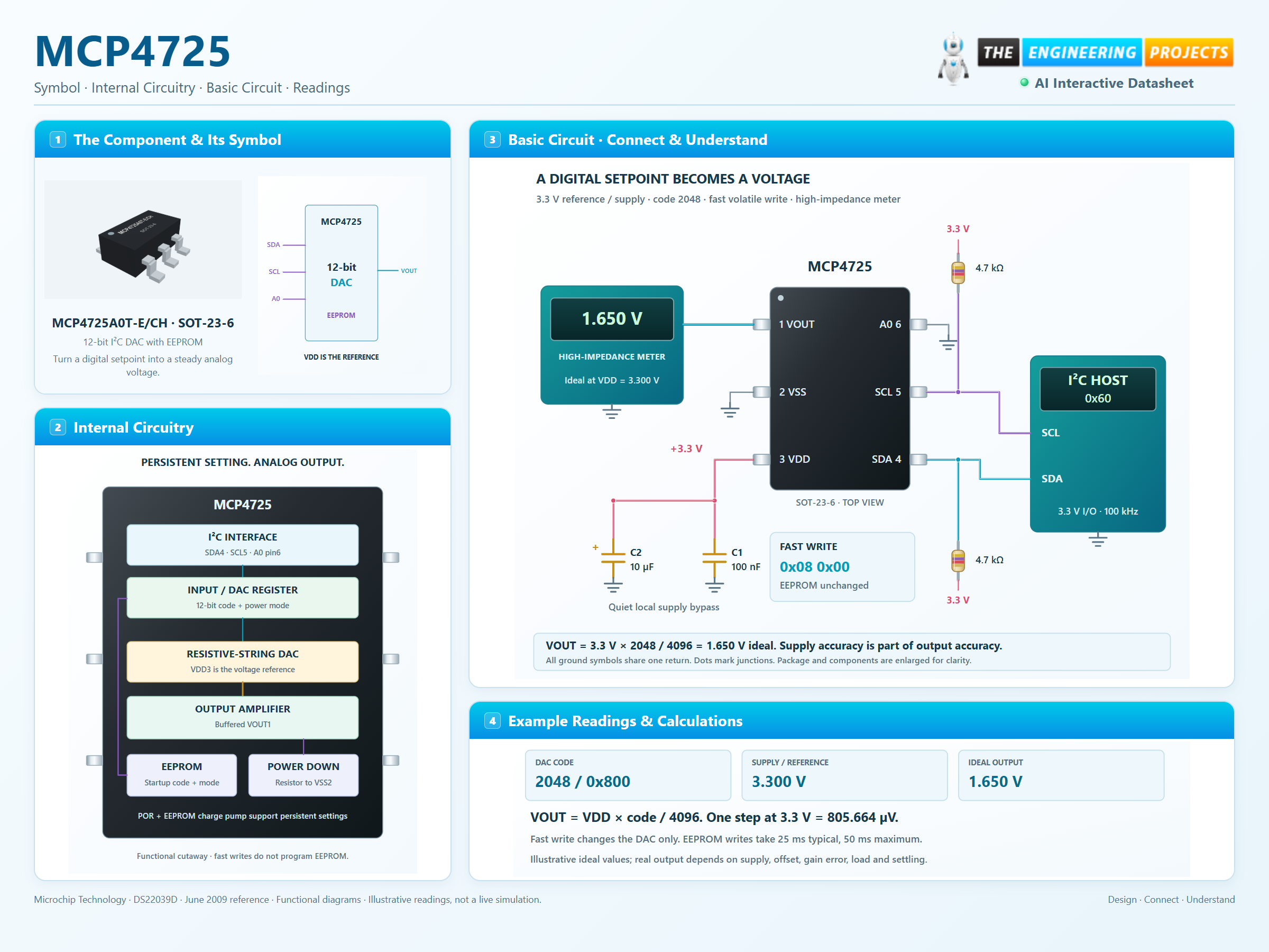
How it works
3 stages · Explore one step at a time
Power a clean reference
Use 3.3 V at VDD and a common ground. Local 100 nF and 10 µF bypass capacitors reduce supply disturbance.
Write the midpoint
At seven-bit address 0x60, the fast-write data bytes 0x08 and 0x00 load code 2048 in Normal mode without writing EEPROM.
Measure the output
An ideal 3.3 V × 2048 / 4096 gives 1.650 V at VOUT. A high-impedance meter avoids excessive loading.
Step 1 of 3
MCP4725 in a circuit
A six-pin IC, quiet supply and an I²C controller.
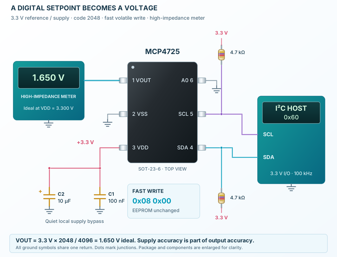
Connect it, step by step
Follow the component values and pin connections
Power and bypass
Connect VDD and VSS to a clean 3.3 V rail and ground with local bypassing.
Send a volatile command
Write fast-mode bytes 0x08 and 0x00 to address 0x60.
Check the analog output
Use a high-impedance meter at VOUT; account for the actual supply and DAC errors.
Inside MCP4725
Serial control, persistent startup data and one buffered analog output.
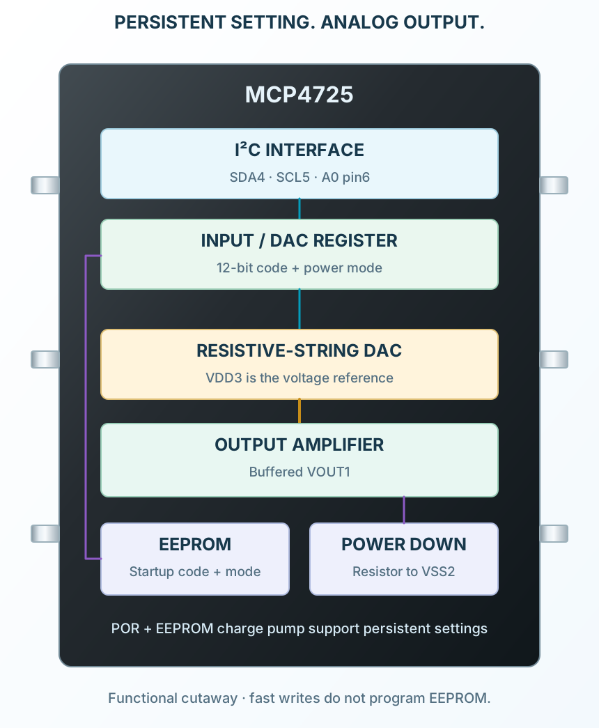
Explore the circuit
Select a stage to see its role and connections
Receive the code
The serial interface accepts the command and twelve-bit output setting.
Select the voltage
A resistive-string DAC uses VDD as its reference.
Buffer or power down
The output amplifier drives VOUT in Normal mode; power-down selects a resistor to ground.
Selected packageSOT-23-6MCP4725A0T-E/CH
Physical connections6 pinsPackage-specific numbering
Reference collection8 tables44 parameters & pin functions
Pin reference
Signal names, electrical functions and connection guidance
Physical pin numbers6 pins
Scroll within the table to see all columns and rows.
| Pin | Signal | Type | Function & connection |
|---|---|---|---|
| VOUT | Buffered analog output | Outputs the voltage selected by the 12-bit DAC code.Connection guidanceConnect a high-impedance meter or suitable analog load. The ideal scale uses VDD / 4096. Loading, offset, gain error and output headroom affect real results. | |
| VSS | Ground | Supply and analog-output reference.Connection guidanceJoin controller ground and measurement return. | |
| VDD | Supply and DAC reference | The supply also determines the output conversion scale.Connection guidanceUse a clean 3.3 V rail, with 100 nF and local bulk bypass to VSS. Supply noise and supply error directly affect the analog output. | |
| SDA | I²C serial data | Bidirectional open-drain data connection.Connection guidanceConnect to controller SDA and a pull-up to VDD. | |
| SCL | I²C serial clock | Clock connection for the I²C controller.Connection guidanceConnect to controller SCL and a pull-up to VDD. | |
| A0 | Address selection | Sets the least-significant address bit; two upper address bits are factory options.Connection guidanceTie LOW for 0x60 on the selected A0 orderable, or HIGH for 0x61. Do not confuse the external A0 pin with the A0 suffix in the ordering code. |
No pins match these filters. Try another signal name or reset the filters.
Operating and interface limits
Extended-temperature grade
Manufacturer-referenced values7 parameters
Scroll within the table to see all columns and rows.
| Parameter | Value | Conditions / notes |
|---|---|---|
| Supply / DAC reference | 2.7–5.5 V | Same VDD pin for power and conversion scale |
| Operating ambient | −40 to +125°C | Selected E grade |
| Code range | 0–4095 | Unsigned 12-bit code |
| I²C modes | 100 kHz, 400 kHz, 3.4 MHz | High-speed mode requires its specified protocol |
| SDA/SCL input HIGH / LOW | ≥ 0.7 VDD / ≤ 0.3 VDD | Use compatible logic levels |
| A0 input HIGH / LOW | ≥ 0.8 VDD / ≤ 0.2 VDD | Different from SDA/SCL thresholds |
| Supply current | 210 µA typical / 400 µA maximum | Code zero; digital inputs grounded; VOUT unloaded |
No specifications match. Try a parameter name or a unit.
Absolute maximum supply is a stress rating and must not replace the recommended operating range.
Ideal transfer at 3.3 V
VOUT = VDD × code / 4096
Manufacturer-referenced values6 parameters
Scroll within the table to see all columns and rows.
| Parameter | Value | Conditions / notes |
|---|---|---|
| Code 0 / 0x000 | 0 V ideal | Real zero-scale offset remains |
| Code 1 / 0x001 | 0.000805664 V | One ideal LSB |
| Code 1024 / 0x400 | 0.825 V | Quarter-scale |
| Code 2048 / 0x800 | 1.650 V | Midscale example |
| Code 3072 / 0xC00 | 2.475 V | Three-quarter scale |
| Code 4095 / 0xFFF | 3.299194 V | One ideal LSB below VDD |
No specifications match. Try a parameter name or a unit.
A rail-to-rail amplifier is still affected by load and headroom near either supply.
I²C command examples
Selected A0 factory option; external A0 LOW
Manufacturer-referenced values7 parameters
Scroll within the table to see all columns and rows.
| Parameter | Value | Conditions / notes |
|---|---|---|
| Seven-bit address | 0x60 | 0xC0 write / 0xC1 read are address bytes, not seven-bit addresses |
| External A0 HIGH | 0x61 | Other factory options provide the remaining address pairs |
| Fast write, midpoint | Data bytes 0x08 0x00 | PD=00; code=0x800; EEPROM unchanged |
| DAC-register write | Data bytes 0x40 0x80 0x00 | Same code via three-byte command format |
| DAC + EEPROM write | Data bytes 0x60 0x80 0x00 | Intentional persistent startup setting |
| Read sequence | Five data bytes after the address | Current status, DAC code and EEPROM content |
| RDY/BSY status | 1 ready; 0 EEPROM write in progress | Returned status bit; no separate ready pin |
No specifications match. Try a parameter name or a unit.
Do not send new write commands during an EEPROM write. Check the returned ready status first.
EEPROM and power modes
Preserve endurance by choosing the correct command
Manufacturer-referenced values6 parameters
Scroll within the table to see all columns and rows.
| Parameter | Value | Conditions / notes |
|---|---|---|
| EEPROM write duration | 25 ms typical / 50 ms maximum | Poll RDY/BSY rather than assuming immediate completion |
| EEPROM endurance | 1 million cycles minimum at +25°C | Design-assured parameter, not 100% tested |
| Data retention | 200 years typical at +25°C | Temperature and conditions matter |
| Startup | Loads stored code and mode | Observe the specified VDD ramp conditions |
| PD 00 | Normal output buffer | DAC output enabled |
| PD 01 / 10 / 11 | 1 kΩ / 100 kΩ / 500 kΩ to ground | Typical output resistance with amplifier powered down |
No specifications match. Try a parameter name or a unit.
Nonvolatile memory is for remembered settings, not continuous waveform updates.
Accuracy and dynamic behavior
Datasheet test conditions apply
Manufacturer-referenced values6 parameters
Scroll within the table to see all columns and rows.
| Parameter | Value | Conditions / notes |
|---|---|---|
| INL | ±2 LSB typical / ±14.5 LSB maximum | Test codes 100–4000 |
| DNL | ±0.2 LSB typical / ±0.75 LSB limits | Test codes 100–4000 |
| Offset error | 0.02% typical / 0.75% maximum FSR | Code zero |
| Gain error | −0.1% typical / ±2% limits FSR | Code 4095; excludes offset |
| Settling time | 6 µs typical | 0x400→0xC00; within half LSB; RL 5 kΩ, CL 100 pF |
| Supply dependence | VDD is the reference | Supply changes scale every nonzero code |
No specifications match. Try a parameter name or a unit.
Typical values are not guarantees. Resolution and absolute accuracy are different properties.
Midscale voltage-output circuit
3.3 V logic and a high-impedance measurement
Manufacturer-referenced values6 parameters
Scroll within the table to see all columns and rows.
| Parameter | Value | Conditions / notes |
|---|---|---|
| VDD3 / VSS2 | 3.3 V / GND | 100 nF plus 10 µF local bypass |
| A0 pin 6 | GND | Address 0x60 for the selected factory option |
| SDA4 / SCL5 | Controller bus | Example 4.7 kΩ pull-ups to 3.3 V; 100 kHz |
| VOUT1 | High-impedance meter | Meter return joins VSS |
| Write | 0x08, 0x00 after address + W | Fast volatile update, Normal mode |
| Expected output | 1.650 V ideal | Measure actual VDD when checking the result |
No specifications match. Try a parameter name or a unit.
Use a suitable external buffer for loads beyond the DAC output’s intended capability.
Package and layout
MCP4725A0T-E/CH · SOT-23-6
Manufacturer-referenced values6 parameters
Scroll within the table to see all columns and rows.
| Parameter | Value | Conditions / notes |
|---|---|---|
| Lead pitch | 0.95 mm | Six gullwing leads; three on each side |
| Nominal visual body | 1.6 × 2.9 mm | Manufacturer tolerance range applies |
| Original footprint | 1.10 × 0.60 mm lands | 2.70 mm pad-row centers; engineering starting point |
| Top marking | AJ plus trace code for A0 option | Illustration labels identify the device; actual marking is abbreviated |
| Supply bypass | Close to pins 3 and 2 | Keep output and ground paths quiet |
| Load connection | Low leakage, suitable impedance | Avoid long capacitive output wiring |
No specifications match. Try a parameter name or a unit.
Verify the selected package, pad dimensions and assembly process before PCB manufacture.
No matching rowsTry a pin name, parameter, unit or test condition, or reset the filters.
Analog setpoints
Set a reference voltage for a compatible control input.
Manufacturer application guideCalibration offsets
Provide an adjustable voltage within a calibrated measurement system.
Manufacturer application guideRemembered startup levels
Store a deliberate startup output while using volatile writes for normal adjustments.
Manufacturer application guideTake it into ProTech
Find MCP4725 in the Components Library to place its schematic symbol and connect its pins.
Reference page · circuit simulation model not yet availableOpen ProTech