Real View
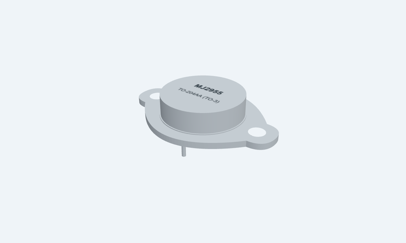
A controlled current path, with every terminal identified.
MJ2955 is a PNP power transistor in a metal TO-204AA (TO-3) package. The two insulated leads are base 1 and emitter 2; the metal case itself is collector. Both mounting contacts share that collector connection. The 15 A collector rating is an absolute limit. Usable current also depends on base drive, safe operating area and heat removal. The pin diagram explicitly shows the bottom view, while the authored PCB pattern uses the top view. The example switches a modest 12 V, 100 Ω load with a buffered driver. Calculated readings assume 0.8 V base-emitter and 0.2 V collector-emitter magnitudes, not guaranteed voltage drops. Only the verified metal package is offered.
Select a pin to explore its connection
Click a lead or use the arrow keys. Bottom view · B1, E2 · case C3
Current-driven control junction.
Use the example’s 330 Ω series drive and 10 kΩ base-emitter return.
Bottom view of CASE 1-07: base 1 below emitter 2, offset toward the left mounting hole.
Reference terminal for base drive.
Connect to +12 V.
Bottom view of CASE 1-07: base 1 below emitter 2, offset toward the left mounting hole.
The metal case is the collector; there is no third wire lead.
Connect to the 100 Ω load above ground.
Both mounting contacts belong to collector. Insulate the heatsink when required.
The mounting case is electrically live. The two silver leads are base and emitter; do not assume the case is ground.
MJ2955 · TO-204AA (TO-3)
| Property | Details |
|---|---|
| Manufacturer | onsemi |
| Part number | MJ2955 |
| Package | TO-204AA (TO-3) |
| Connections | 3 pins |
| Mounting | Through-hole |
| Lead pitch | 10.92 mm lead spacing |
| Package code | CASE 1-07 |
| Thermal reference | 115 W at case 25°C; heatsink required |
Selected manufacturer reference
Scroll sideways to see all columns.
| Parameter | Value | Conditions / notes |
|---|---|---|
| Device | MJ2955 | onsemi complementary power transistor family |
| Polarity | PNP | Voltages and currents below use magnitudes |
| Physical connection | B1 · E2 · case C3 | Two insulated TO-3 leads; case is collector |
| Package | TO-204AA (TO-3) | CASE 1-07, style 1 |
No specifications match. Try a parameter name or a unit.
No unverified SMD substitute is selected.
Do not combine maxima into one operating point
Scroll sideways to see all columns.
| Parameter | Value | Conditions / notes |
|---|---|---|
| Collector-emitter VCEO | 60 V | Open base |
| Collector-emitter VCER | 70 V | 100 Ω base-emitter resistor |
| Collector-base voltage | 100 V | Absolute maximum |
| Emitter-base reverse voltage | 7 V | Absolute maximum |
| Collector / base current | 15 A / 7 A | Absolute maximum |
| Dissipation | 115 W at case 25°C | Derate 0.657 W/°C |
| Junction / storage | −65 to +200°C | Absolute limits |
No specifications match. Try a parameter name or a unit.
Apply the manufacturer safe operating area.
25°C and stated manufacturer conditions
Scroll sideways to see all columns.
| Parameter | Value | Conditions / notes |
|---|---|---|
| DC gain at 4 A | 20–70 | VCE magnitude 4 V |
| DC gain at 10 A | 5 minimum | VCE magnitude 4 V |
| Saturation at 4 A / 400 mA base | 1.1 V maximum | Case 25°C |
| Saturation at 10 A / 3.3 A base | 3 V maximum | Case 25°C |
| Base-emitter on voltage | 1.5 V maximum | IC magnitude 4 A; VCE magnitude 4 V |
No specifications match. Try a parameter name or a unit.
PNP test currents and voltages are negative in the source; magnitudes are shown.
Case and ambient conditions differ
Scroll sideways to see all columns.
| Parameter | Value | Conditions / notes |
|---|---|---|
| Junction-to-case | 1.52°C/W maximum | Controlled case |
| Mounting centres | 30.15 mm | Collector case |
| Base/emitter spacing | 10.92 mm | CASE 1-07 |
| Lead diameter | 0.97–1.09 mm | Two insulated leads |
No specifications match. Try a parameter name or a unit.
The authored footprint is a starting pattern, not a manufacturer land recommendation.
Explicit low-current teaching assumptions
Scroll sideways to see all columns.
| Parameter | Value | Conditions / notes |
|---|---|---|
| Supply and load | 12 V / 100 Ω ≥3 W | Resistive load |
| Buffered driver | 12 V off / 7 V on | 330 Ω base resistor |
| Base-emitter return | 10 kΩ | Defined off state |
| Assumed junction drops | |VBE| 0.8 V / |VCE| 0.2 V | Illustrative only |
| Collector / base current | 118 mA / 12.65 mA | Includes base-return current |
| Device / load power | 33.7 mW / 1.392 W | Includes base-emitter input power |
No specifications match. Try a parameter name or a unit.
Do not infer high-current capability from this small example.
Select a pin for its function, connection guidance and electrical notes.
Follow the labeled connections and functional stages
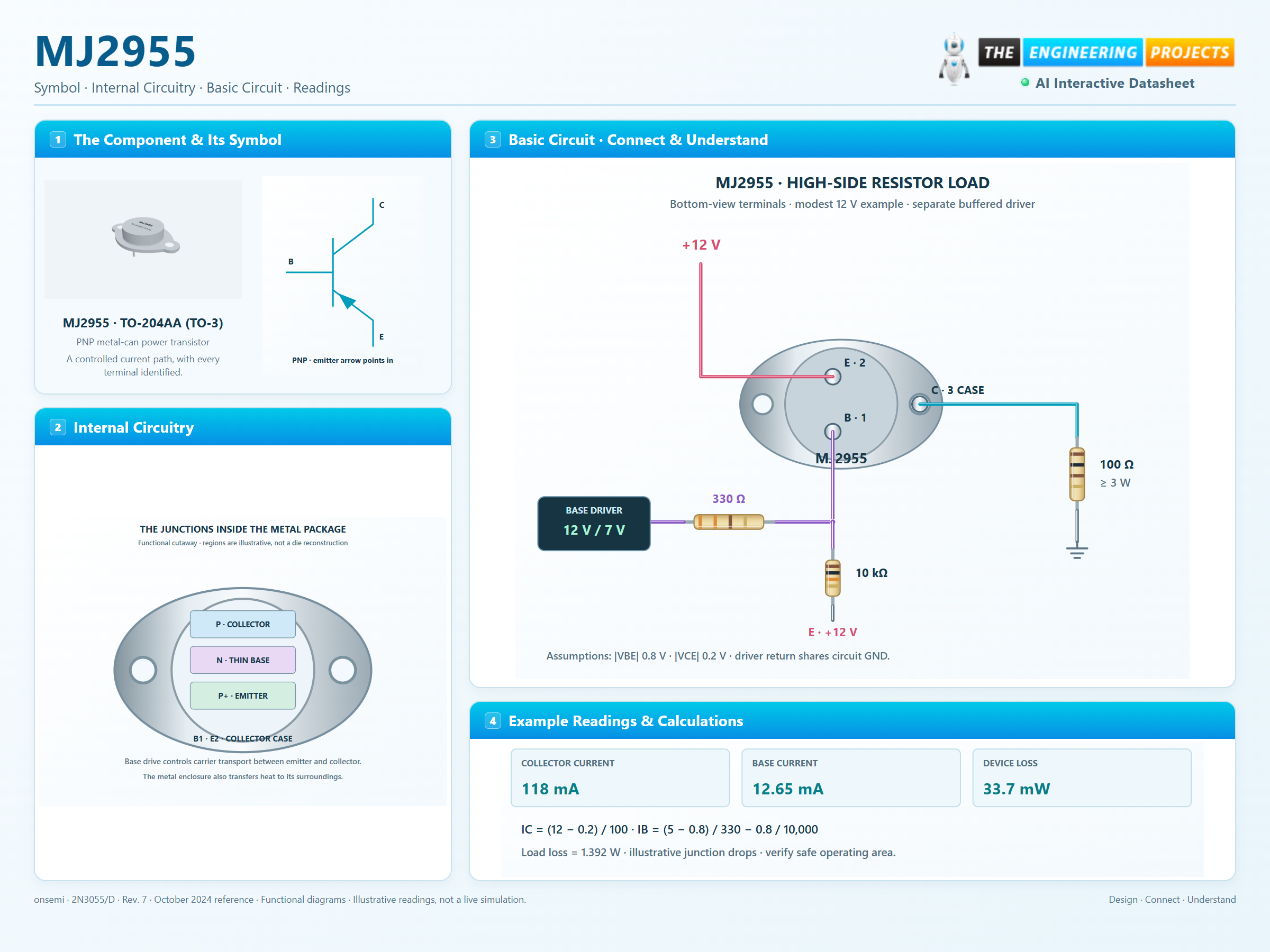
3 stages · Explore one step at a time
Pull base below emitter through the resistor. The driver must return to +12 V to turn off.
Conventional current enters emitter and leaves collector.
Check safe operating area, drive current and cooling together; a current rating is not a guaranteed operating point.
A modest resistor load with explicit buffered base drive.
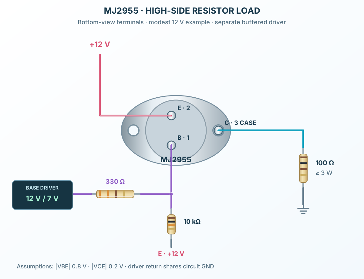
Follow the component values and pin connections
Pull base below emitter through the resistor. The driver must return to +12 V to turn off.
Conventional current enters emitter and leaves collector.
Check safe operating area, drive current and cooling together; a current rating is not a guaranteed operating point.
Compact functional cutaway inside the metal package.
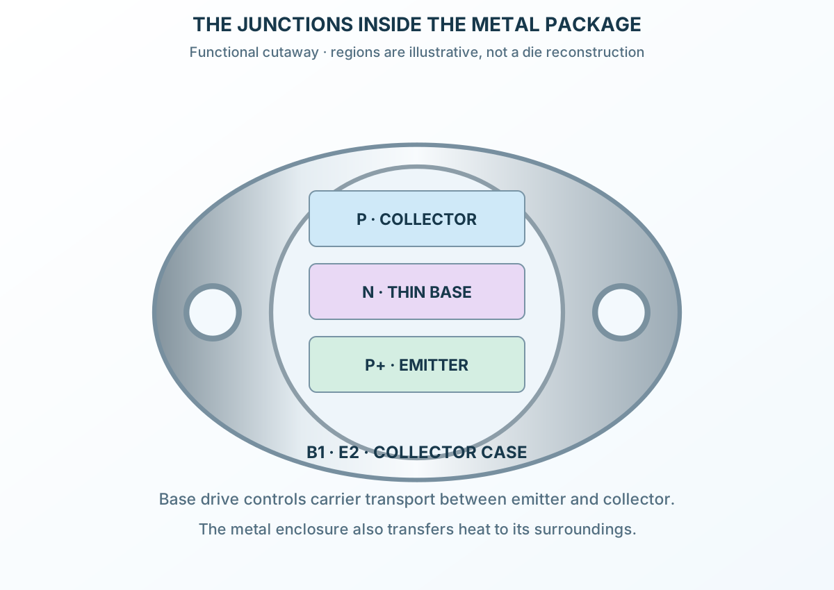
Select a stage to see its role and connections
Pull base below emitter through the resistor. The driver must return to +12 V to turn off.
Conventional current enters emitter and leaves collector.
Check safe operating area, drive current and cooling together; a current rating is not a guaranteed operating point.
Signal names, electrical functions and connection guidance
Scroll within the table to see all columns and rows.
| Pin | Signal | Type | Function & connection |
|---|---|---|---|
| B | Base | Current-driven control junction.Connection guidanceUse the example’s 330 Ω series drive and 10 kΩ base-emitter return. Bottom view of CASE 1-07: base 1 below emitter 2, offset toward the left mounting hole. | |
| E | Emitter | Reference terminal for base drive.Connection guidanceConnect to +12 V. Bottom view of CASE 1-07: base 1 below emitter 2, offset toward the left mounting hole. | |
| C | Collector | The metal case is the collector; there is no third wire lead.Connection guidanceConnect to the 100 Ω load above ground. Both mounting contacts belong to collector. Insulate the heatsink when required. |
No pins match these filters. Try another signal name or reset the filters.
Selected manufacturer reference
Scroll within the table to see all columns and rows.
| Parameter | Value | Conditions / notes |
|---|---|---|
| Device | MJ2955 | onsemi complementary power transistor family |
| Polarity | PNP | Voltages and currents below use magnitudes |
| Physical connection | B1 · E2 · case C3 | Two insulated TO-3 leads; case is collector |
| Package | TO-204AA (TO-3) | CASE 1-07, style 1 |
No specifications match. Try a parameter name or a unit.
No unverified SMD substitute is selected.
Do not combine maxima into one operating point
Scroll within the table to see all columns and rows.
| Parameter | Value | Conditions / notes |
|---|---|---|
| Collector-emitter VCEO | 60 V | Open base |
| Collector-emitter VCER | 70 V | 100 Ω base-emitter resistor |
| Collector-base voltage | 100 V | Absolute maximum |
| Emitter-base reverse voltage | 7 V | Absolute maximum |
| Collector / base current | 15 A / 7 A | Absolute maximum |
| Dissipation | 115 W at case 25°C | Derate 0.657 W/°C |
| Junction / storage | −65 to +200°C | Absolute limits |
No specifications match. Try a parameter name or a unit.
Apply the manufacturer safe operating area.
25°C and stated manufacturer conditions
Scroll within the table to see all columns and rows.
| Parameter | Value | Conditions / notes |
|---|---|---|
| DC gain at 4 A | 20–70 | VCE magnitude 4 V |
| DC gain at 10 A | 5 minimum | VCE magnitude 4 V |
| Saturation at 4 A / 400 mA base | 1.1 V maximum | Case 25°C |
| Saturation at 10 A / 3.3 A base | 3 V maximum | Case 25°C |
| Base-emitter on voltage | 1.5 V maximum | IC magnitude 4 A; VCE magnitude 4 V |
No specifications match. Try a parameter name or a unit.
PNP test currents and voltages are negative in the source; magnitudes are shown.
Case and ambient conditions differ
Scroll within the table to see all columns and rows.
| Parameter | Value | Conditions / notes |
|---|---|---|
| Junction-to-case | 1.52°C/W maximum | Controlled case |
| Mounting centres | 30.15 mm | Collector case |
| Base/emitter spacing | 10.92 mm | CASE 1-07 |
| Lead diameter | 0.97–1.09 mm | Two insulated leads |
No specifications match. Try a parameter name or a unit.
The authored footprint is a starting pattern, not a manufacturer land recommendation.
Explicit low-current teaching assumptions
Scroll within the table to see all columns and rows.
| Parameter | Value | Conditions / notes |
|---|---|---|
| Supply and load | 12 V / 100 Ω ≥3 W | Resistive load |
| Buffered driver | 12 V off / 7 V on | 330 Ω base resistor |
| Base-emitter return | 10 kΩ | Defined off state |
| Assumed junction drops | |VBE| 0.8 V / |VCE| 0.2 V | Illustrative only |
| Collector / base current | 118 mA / 12.65 mA | Includes base-return current |
| Device / load power | 33.7 mW / 1.392 W | Includes base-emitter input power |
No specifications match. Try a parameter name or a unit.
Do not infer high-current capability from this small example.
No matching rowsTry a pin name, parameter, unit or test condition, or reset the filters.
Control loads within the electrical and thermal ratings.
Manufacturer application guideChoose bias and a safe operating point rather than assuming saturation behavior.
Manufacturer application guideMatch the exact voltage grade, polarity, lead order and case connection before substituting a part.
Manufacturer application guideFind MJ2955 in the Components Library to place its schematic symbol and connect its pins.
Reference page · circuit simulation model not yet availableOpen ProTech