MOC3063Zero-cross optotriac driver
Light transfers the command. Zero-cross logic chooses the turn-on window.
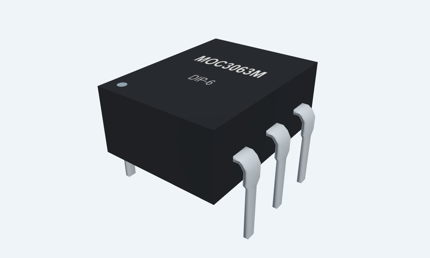
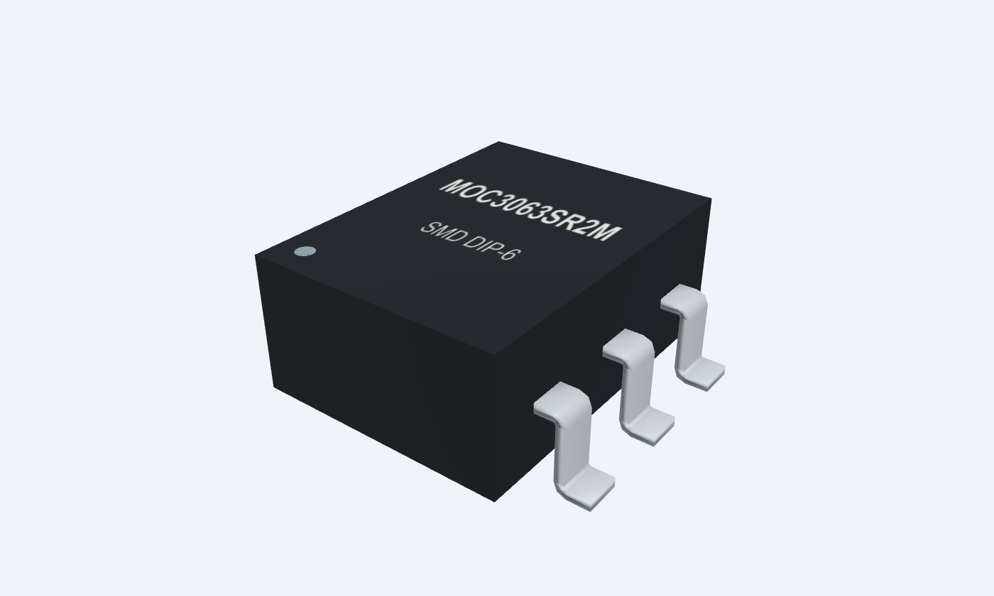
MOC3063 is an optically isolated triac-driver family. An infrared LED transfers a command to a bilateral output switch without a conductive signal connection between the two sides. The selected onsemi MOC3063M has a 600 V peak off-state output rating. Its zero-cross circuit inhibits triggering while the output voltage is too large. This suits whole-cycle AC switching, but it is not a random-phase dimmer driver. The 5 mA maximum trigger-current test is specified at 3 V across the main terminals and 25°C. Both DIP MOC3063M and gullwing MOC3063SR2M SMD versions retain all six physical pins. Pin 3 is unused and pin 5 is a substrate connection that must remain open. The example uses a small isolated AC source and resistor load to explain optical switching without a mains connection.

6Physical pins
MOC3063MDIP-6
Manufacturer-referencedonsemi
Pin diagram
Select a pin to explore its connection
Highlight
MOC3063MDIP-6Top view · dot marks LED anode pin 1
MOC3063SMD DIP-6Top view · dot marks LED anode pin 1
Click a lead or use the arrow keys. Top view · dot marks LED anode pin 1
PIN 1 · Infrared input
Infrared LED anodeA
Function
Positive terminal of the optical input emitter.
How to connect
Use a buffered 5 V source through 560 Ω.
Electrical note
Drive above the required trigger current with temperature and tolerance margin.
PIN 2 · Infrared input
Infrared LED cathodeK
Function
Input-side return for the emitter current.
How to connect
Return to GND_A.
Electrical note
Do not join the input return to the isolated output domain.
PIN 3 · Not connected
Not connectedNC
Function
No intended internal connection.
How to connect
Leave unconnected.
PIN 4 · Isolated bilateral output
Main output terminalMT
Function
One terminal of the light-triggered bilateral switch.
How to connect
Connect to the isolated AC source return in the example.
Electrical note
This is a triac driver, not a high-power load switch.
PIN 5 · Leave open
Do not connectDNC
Function
Internal triac substrate lead.
How to connect
Leave open; do not route a signal through this pin.
Electrical note
NC in the manufacturer symbol does not authorize connecting this substrate lead.
PIN 6 · Isolated bilateral output
Main output terminalMT
Function
Other terminal of the light-triggered bilateral switch.
How to connect
Connect through the pulse/load resistor to the isolated AC source.
Electrical note
The zero-cross inhibit circuit delays triggering until a sufficiently small output voltage.
Key specifications
The detector requires both sufficient optical drive and a low enough output-terminal voltage. Removing LED current does not force an already-conducting triac path off.
Output blocking600 V peak · absolute
LED trigger max.5 mA · specified conditions
Ambient range−40–85 °C
Isolation test4.17 kVrms · one minute
Package details
MOC3063M · DIP-6
| Property | Details |
|---|---|
| Manufacturer | onsemi |
| Part number | MOC3063M |
| Package | DIP-6 |
| Connections | 6 pins |
| Mounting | Through-hole |
| Lead pitch | 2.54 mm |
| Package code | 646BX |
| Thermal reference | Apply separate input, detector and total package power limits. |
Device and pin connections
Selected onsemi family
Manufacturer specifications 5 parameters
Scroll sideways to see all columns.
| Parameter | Value | Conditions / notes |
|---|---|---|
| Through-hole / surface-mount | MOC3063M / MOC3063SR2M | 646BX / formed 646BY |
| Input | 1 anode · 2 cathode | Current limiting required |
| Output | Main terminals 4 and 6 | Bilateral triac-driver output |
| Leave open | Pin 3 NC · pin 5 substrate | Never use pin 5 as a wiring junction |
| Trigger type | Zero-cross | Not suitable for arbitrary phase-angle turn-on |
No specifications match. Try a parameter name or a unit.
Read the selected manufacturer’s variant rather than assuming all similar part names match.
Absolute maximum ratings
Ambient 25°C unless noted
Manufacturer specifications 7 parameters
Scroll sideways to see all columns.
| Parameter | Value | Conditions / notes |
|---|---|---|
| Emitter continuous / reverse | 60 mA / 6 V | Separate stress limits |
| Output blocking | 600 V peak | Either direction |
| Output surge | 1 A single 60 Hz cycle | Not continuous load current |
| Repetitive output peak | 100 mA | Separate from surge rating |
| Input / detector dissipation | 120 / 150 mW | Derate above 25°C |
| Total dissipation | 250 mW | Combined input and detector limit |
| Ambient / junction max. | −40 to +85°C / +100°C | Storage −40 to +125°C |
No specifications match. Try a parameter name or a unit.
A driver output must not be used as a mains power switch.
Electrical characteristics
TA 25°C; selected device
Manufacturer specifications 6 parameters
Scroll sideways to see all columns.
| Parameter | Value | Conditions / notes |
|---|---|---|
| LED forward voltage | 1.3 V typical; 1.5 V maximum | IF 30 mA |
| LED trigger current | 5 mA maximum | Main-terminal voltage 3 V |
| Peak on-state voltage | 1.8 V typical; 3 V maximum | ITM 100 mA; IF at rated trigger |
| Holding current | 500 µA typical | Either direction |
| Off-state leakage | 10 nA typical; 500 nA maximum | Rated blocking voltage; input off |
| Static dV/dt | 600 V/µs minimum; 1500 typical | Input off; specified rated-voltage test |
No specifications match. Try a parameter name or a unit.
The low-current demonstration uses an explicit drop assumption.
Zero-cross inhibition
MOC3063M, not the lower-threshold MOC3163M
Manufacturer specifications 4 parameters
Scroll sideways to see all columns.
| Parameter | Value | Conditions / notes |
|---|---|---|
| Inhibit voltage | 12 V typical; 20 V maximum | Above this output voltage the device will not trigger; IF rated |
| Inhibited leakage | 2 mA maximum | 600 V output; IF rated |
| Optical command already on | Wait for eligible low-voltage window | No immediate arbitrary-phase turn-on |
| Turn-off | Load current must fall below holding level | Input off prevents retrigger after commutation |
No specifications match. Try a parameter name or a unit.
These voltage thresholds do not specify an exact time delay.
Isolation and mounting
Device certification does not certify the assembled board
Manufacturer specifications 6 parameters
Scroll sideways to see all columns.
| Parameter | Value | Conditions / notes |
|---|---|---|
| Input-output dielectric test | 4170 Vrms · 1 minute | Test condition, not continuous working voltage |
| External creepage / clearance | ≥7 mm / ≥7 mm | Selected standard package; check installed board |
| Body | 8.51 × 6.35 mm nominal | 2.54 mm pitch; 3.40 mm nominal mould height |
| DIP footprint | 7.62 mm rows | Original 1 mm holes, 1.8 mm pads |
| SMD recommended lands | 1.525 × 1.78 mm | 9.015 mm rows; 10.54 mm outer span |
| Isolation layout | Keep both domains separate | Slots, copper, contamination and enclosure affect the system |
No specifications match. Try a parameter name or a unit.
Use the relevant safety approval option and complete system insulation design.
Isolated low-current AC demonstration
Buffered input and separate isolated output source
Manufacturer specifications 7 parameters
Scroll sideways to see all columns.
| Parameter | Value | Conditions / notes |
|---|---|---|
| Input source / resistor | 5 V_A / 560 Ω | Input switch or buffer must source the LED current |
| Nominal LED current | 6.61 mA | Assumed VF 1.3 V |
| At 1.5 V LED drop | 6.25 mA | Nominal supply/resistor only; temperature and tolerance remain |
| Output source / load | 12 V RMS isolated / 2.2 kΩ | Resistor ≥0.25 W |
| Approximate peak load | 6.90 mA | (12√2−1.8)/2200; assumed output drop |
| Resistor power upper bound | 65.5 mW | 12²/2200; neglects device drop |
| Returns | GND_A isolated from AC_B | No wire crosses the barrier |
No specifications match. Try a parameter name or a unit.
Calculated teaching values, not a measured switching waveform.
Connections by function
Select a pin for its function, connection guidance and electrical notes.
Infrared input2 pins
Not connected1 pin
Isolated bilateral output2 pins
Leave open1 pin
Infrared input2 pins
Not connected1 pin
Isolated bilateral output2 pins
Leave open1 pin
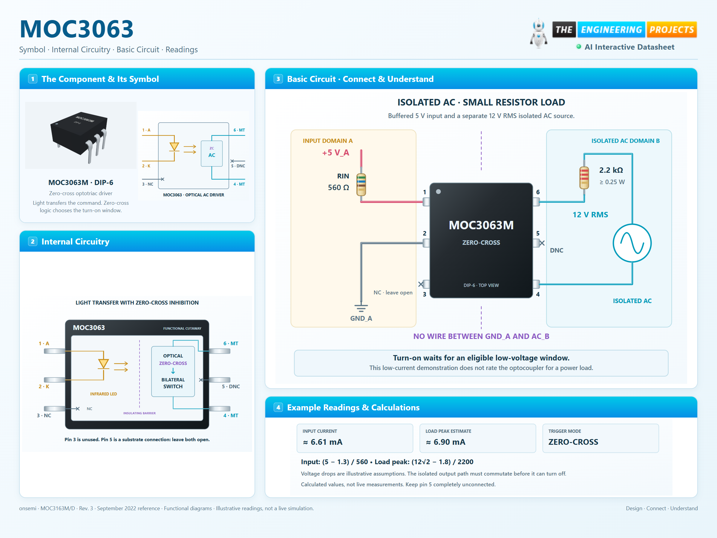
MOC3063 at a glance
Follow the labeled connections and functional stages
How it works
3 stages · Explore one step at a time
Drive the emitter
The buffered source and resistor set infrared LED current.
Wait near the crossing
The optical detector permits triggering only inside the low-output-voltage window.
Allow current commutation
The output remains conducting until current falls sufficiently; removing LED drive prevents later retriggering.
Step 1 of 3
MOC3063 in a circuit
Physical six-pin package with both no-connect leads marked.
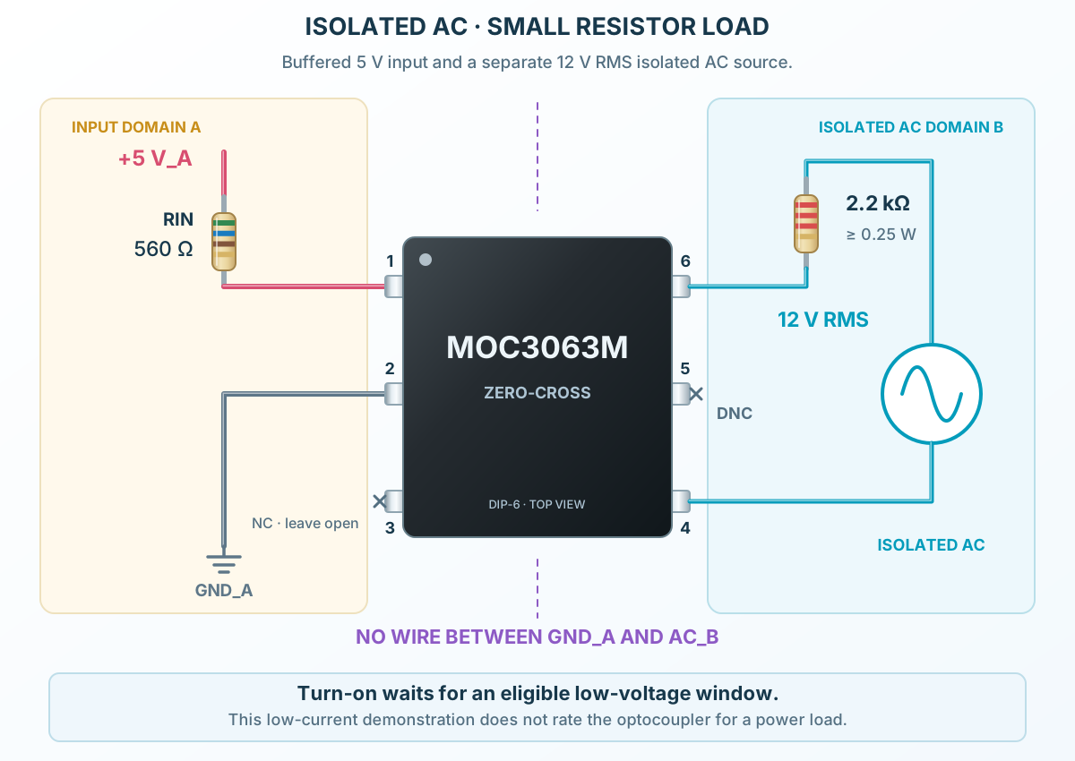
Connect it, step by step
Follow the component values and pin connections
Set input current
Use 560 Ω from the buffered 5 V source to pin 1.
Keep returns separate
Input cathode goes only to GND_A; the AC source stays isolated.
Observe output
A 2.2 kΩ resistor limits the output current to a few milliamps.
Inside MOC3063
Infrared emitter, zero-cross detector and bilateral switch.
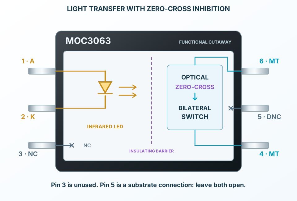
Explore the circuit
Select a stage to see its role and connections
Optical input
The LED converts current into infrared light.
Insulating barrier
Only the optical signal crosses the package barrier.
Bilateral output
Zero-cross inhibition qualifies turn-on; output current controls turn-off.
Selected packageDIP-6MOC3063M
Physical connections6 pinsPackage-specific numbering
Reference collection7 tables35 parameters & pin functions
Pin reference
Signal names, electrical functions and connection guidance
Physical pin numbers6 pins
Scroll within the table to see all columns and rows.
| Pin | Signal | Type | Function & connection |
|---|---|---|---|
| A | Infrared LED anode | Positive terminal of the optical input emitter.Connection guidanceUse a buffered 5 V source through 560 Ω. Drive above the required trigger current with temperature and tolerance margin. | |
| K | Infrared LED cathode | Input-side return for the emitter current.Connection guidanceReturn to GND_A. Do not join the input return to the isolated output domain. | |
| NC | Not connected | No intended internal connection.Connection guidanceLeave unconnected. | |
| MT | Main output terminal | One terminal of the light-triggered bilateral switch.Connection guidanceConnect to the isolated AC source return in the example. This is a triac driver, not a high-power load switch. | |
| DNC | Do not connect | Internal triac substrate lead.Connection guidanceLeave open; do not route a signal through this pin. NC in the manufacturer symbol does not authorize connecting this substrate lead. | |
| MT | Main output terminal | Other terminal of the light-triggered bilateral switch.Connection guidanceConnect through the pulse/load resistor to the isolated AC source. The zero-cross inhibit circuit delays triggering until a sufficiently small output voltage. |
No pins match these filters. Try another signal name or reset the filters.
Device and pin connections
Selected onsemi family
Manufacturer-referenced values5 parameters
Scroll within the table to see all columns and rows.
| Parameter | Value | Conditions / notes |
|---|---|---|
| Through-hole / surface-mount | MOC3063M / MOC3063SR2M | 646BX / formed 646BY |
| Input | 1 anode · 2 cathode | Current limiting required |
| Output | Main terminals 4 and 6 | Bilateral triac-driver output |
| Leave open | Pin 3 NC · pin 5 substrate | Never use pin 5 as a wiring junction |
| Trigger type | Zero-cross | Not suitable for arbitrary phase-angle turn-on |
No specifications match. Try a parameter name or a unit.
Read the selected manufacturer’s variant rather than assuming all similar part names match.
Absolute maximum ratings
Ambient 25°C unless noted
Manufacturer-referenced values7 parameters
Scroll within the table to see all columns and rows.
| Parameter | Value | Conditions / notes |
|---|---|---|
| Emitter continuous / reverse | 60 mA / 6 V | Separate stress limits |
| Output blocking | 600 V peak | Either direction |
| Output surge | 1 A single 60 Hz cycle | Not continuous load current |
| Repetitive output peak | 100 mA | Separate from surge rating |
| Input / detector dissipation | 120 / 150 mW | Derate above 25°C |
| Total dissipation | 250 mW | Combined input and detector limit |
| Ambient / junction max. | −40 to +85°C / +100°C | Storage −40 to +125°C |
No specifications match. Try a parameter name or a unit.
A driver output must not be used as a mains power switch.
Electrical characteristics
TA 25°C; selected device
Manufacturer-referenced values6 parameters
Scroll within the table to see all columns and rows.
| Parameter | Value | Conditions / notes |
|---|---|---|
| LED forward voltage | 1.3 V typical; 1.5 V maximum | IF 30 mA |
| LED trigger current | 5 mA maximum | Main-terminal voltage 3 V |
| Peak on-state voltage | 1.8 V typical; 3 V maximum | ITM 100 mA; IF at rated trigger |
| Holding current | 500 µA typical | Either direction |
| Off-state leakage | 10 nA typical; 500 nA maximum | Rated blocking voltage; input off |
| Static dV/dt | 600 V/µs minimum; 1500 typical | Input off; specified rated-voltage test |
No specifications match. Try a parameter name or a unit.
The low-current demonstration uses an explicit drop assumption.
Zero-cross inhibition
MOC3063M, not the lower-threshold MOC3163M
Manufacturer-referenced values4 parameters
Scroll within the table to see all columns and rows.
| Parameter | Value | Conditions / notes |
|---|---|---|
| Inhibit voltage | 12 V typical; 20 V maximum | Above this output voltage the device will not trigger; IF rated |
| Inhibited leakage | 2 mA maximum | 600 V output; IF rated |
| Optical command already on | Wait for eligible low-voltage window | No immediate arbitrary-phase turn-on |
| Turn-off | Load current must fall below holding level | Input off prevents retrigger after commutation |
No specifications match. Try a parameter name or a unit.
These voltage thresholds do not specify an exact time delay.
Isolation and mounting
Device certification does not certify the assembled board
Manufacturer-referenced values6 parameters
Scroll within the table to see all columns and rows.
| Parameter | Value | Conditions / notes |
|---|---|---|
| Input-output dielectric test | 4170 Vrms · 1 minute | Test condition, not continuous working voltage |
| External creepage / clearance | ≥7 mm / ≥7 mm | Selected standard package; check installed board |
| Body | 8.51 × 6.35 mm nominal | 2.54 mm pitch; 3.40 mm nominal mould height |
| DIP footprint | 7.62 mm rows | Original 1 mm holes, 1.8 mm pads |
| SMD recommended lands | 1.525 × 1.78 mm | 9.015 mm rows; 10.54 mm outer span |
| Isolation layout | Keep both domains separate | Slots, copper, contamination and enclosure affect the system |
No specifications match. Try a parameter name or a unit.
Use the relevant safety approval option and complete system insulation design.
Isolated low-current AC demonstration
Buffered input and separate isolated output source
Manufacturer-referenced values7 parameters
Scroll within the table to see all columns and rows.
| Parameter | Value | Conditions / notes |
|---|---|---|
| Input source / resistor | 5 V_A / 560 Ω | Input switch or buffer must source the LED current |
| Nominal LED current | 6.61 mA | Assumed VF 1.3 V |
| At 1.5 V LED drop | 6.25 mA | Nominal supply/resistor only; temperature and tolerance remain |
| Output source / load | 12 V RMS isolated / 2.2 kΩ | Resistor ≥0.25 W |
| Approximate peak load | 6.90 mA | (12√2−1.8)/2200; assumed output drop |
| Resistor power upper bound | 65.5 mW | 12²/2200; neglects device drop |
| Returns | GND_A isolated from AC_B | No wire crosses the barrier |
No specifications match. Try a parameter name or a unit.
Calculated teaching values, not a measured switching waveform.
No matching rowsTry a pin name, parameter, unit or test condition, or reset the filters.
Whole-cycle AC control
Choose complete cycles for compatible resistive heating loads with a separately rated power stage.
Manufacturer application guideIsolated triac gates
Separate the low-voltage controller from the power-side trigger network.
Manufacturer application guideTeaching optical isolation
Observe a small isolated AC load while keeping both return domains separate.
Manufacturer application guideTake it into ProTech
Find MOC3063 in the Components Library to place its schematic symbol and connect its pins.
Reference page · circuit simulation model not yet availableOpen ProTech