Real View
Follow the switching path from input energy to a regulated output.
MP1584 is a non-synchronous buck converter with an internal high-side MOSFET. An external inductor, Schottky catch diode and capacitors turn its switching waveform into a lower DC voltage; a resistor divider sets the output around a 0.8 V feedback reference. The eight-lead SOIC-8E package has an exposed ground pad underneath. Its current class is 3 A, subject to component selection, board cooling and operating conditions. This reference is for the IC, rather than a particular adjustable module sold around it. The example uses a regulated 12 V input and a nominal 5 V output, with explicit bootstrap, frequency and compensation connections. MPS marks MP1584 as not recommended for new designs and points to MP2338 as an alternative; this page supports understanding and maintaining existing MP1584 designs.
Select a pin to explore its connection
Click a lead or use the arrow keys. Top view · 8 leads; underside exposed pad = GND5
The internal high-side MOSFET drives this node. The inductor and external catch diode complete the buck power stage.
Connect the inductor to the output and the Schottky cathode to SW; its anode returns to ground.
SW is a noisy switching node, not the regulated DC output.
A high level enables operation; a low level disables it. An open pin also enables the device.
Leave open for the fixed 12 V example, or drive within the specified pin limits.
Typical rising threshold 1.5 V. Do not tie EN directly to a 12 V input; its absolute maximum is 6 V.
Error-amplifier output used to shape the converter feedback loop.
Fit the reviewed series RC network from COMP to ground.
Compensation depends on the inductor, output capacitance, ESR and operating conditions.
The control loop compares the divided output to a nominal 0.8 V reference.
Connect the midpoint of the output-to-ground divider.
Route away from SW and the high-current loop.
Return for control and power circuitry. The exposed underside pad also connects to ground.
Join pin 5 and the exposed pad to a suitable ground plane.
The footprint repeats electrical pad number 5 on the exposed pad; it does not invent a separate signal pin.
A resistor from FREQ to ground sets the switching frequency.
Use 200 kΩ in the approximately 500 kHz example.
The frequency setting is nominal; light-load pulse skipping changes the observed switching activity.
Supplies the internal control and high-side switching stage.
Place a low-ESR input bypass close to VIN and the power return.
Operating input is 4.5–28 V; 30 V is an absolute stress limit, not a working target.
Provides gate-drive supply above the SW node.
Connect 100 nF between BST and SW, with short traces.
Observe the 6 V absolute BST-to-SW limit; this capacitor does not connect to ground.
When the high-side switch turns off, the external Schottky diode provides a path for the inductor current. The output capacitor smooths the voltage while feedback adjusts the switching action.
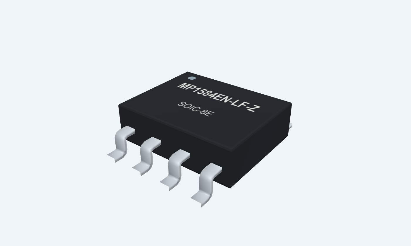
MP1584EN-LF-Z · SOIC-8E
| Property | Details |
|---|---|
| Manufacturer | Monolithic Power Systems |
| Part number | MP1584EN-LF-Z |
| Package | SOIC-8E |
| Connections | 8 pins |
| Mounting | SMD |
| Lead pitch | 1.27 mm |
| Package code | SOIC-8E |
| Thermal reference | −20–85°C ambient; −20–125°C operating junction |
MP1584EN · limits and test conditions
Scroll sideways to see all columns.
| Parameter | Value | Conditions / notes |
|---|---|---|
| Input supply | 4.5–28 V | Recommended operating range |
| Output adjustment | 0.8–25 V | Must remain below input with adequate headroom |
| Output-current class | 3 A | Limited by power components, temperature and layout |
| Operating junction | −20 to +125°C | Do not use shutdown temperature as an operating target |
| Ambient ordering range | −20 to +85°C | MP1584EN package reference |
| Package | SOIC-8E | Eight leads plus a grounded exposed pad |
| Lifecycle note | Not recommended for new designs | MPS identifies MP2338 as an alternative; it is not pin-compatible by assumption |
No specifications match. Try a parameter name or a unit.
Electrical table baseline is VIN = 12 V, VEN = 2.5 V, VCOMP = 1.4 V and TA = 25°C unless stated.
Separate nominal behavior from guaranteed limits
Scroll sideways to see all columns.
| Parameter | Value | Conditions / notes |
|---|---|---|
| Feedback voltage | 0.776 / 0.800 / 0.824 V | Minimum / typical / maximum; 4.5 V < VIN < 28 V |
| High-side on resistance | 150 mΩ typical | BST − SW = 5 V |
| Current-limit threshold | 4.0 A minimum; 4.7 A typical | No maximum is stated here; not a 3 A output guarantee |
| UVLO rising threshold | 2.7 / 3.0 / 3.3 V | Internal threshold; operation still requires the specified input range |
| UVLO hysteresis | 0.35 V typical | Input undervoltage control |
| EN rising threshold | 1.35 / 1.50 / 1.65 V | EN hysteresis 0.30 V typical |
| No-load quiescent current | 100 µA typical; 125 µA maximum | FB = 0.9 V |
| Shutdown current | 12 µA typical; 20 µA maximum | EN = 0 V |
| Soft start | 1.5 ms | Design-guaranteed source value; FB from 0 to 0.8 V |
No specifications match. Try a parameter name or a unit.
Typical values do not establish worst-case performance.
The example follows the 5 V compensation row
Scroll sideways to see all columns.
| Parameter | Value | Conditions / notes |
|---|---|---|
| Programmable frequency | 100 kHz–1.5 MHz | External resistor at FREQ |
| RFREQ relationship | RFREQ[kΩ] = 180000 / f[kHz]^1.1 | Approximate design equation |
| Example RFREQ | 200 kΩ | Approximately 485 kHz by the equation; nominal 500 kHz class |
| Example output inductor | 15 µH | Source table lists 15–22 µH for 5 V / 22 µF output |
| Example output capacitor | 22 µF low-ESR ceramic | Account for capacitance loss under DC bias |
| COMP series network | 100 kΩ and 150 pF to ground | Source 5 V compensation row |
| Extra COMP capacitor | Not fitted in this example | Evaluate separately for high-ESR output capacitors |
No specifications match. Try a parameter name or a unit.
Changing power-stage components can require a new loop-stability review.
Illustrative 1 A load · regulated bench input
Scroll sideways to see all columns.
| Parameter | Value | Conditions / notes |
|---|---|---|
| Input / output | 12 V / 4.984 V nominal | Before reference, resistor and regulation errors |
| Feedback divider | 52.3 kΩ upper; 10 kΩ lower | Use 1% resistors; nominal divider current 80 µA |
| Bootstrap capacitor | 100 nF | Between BST8 and SW1 |
| Input bypass | 10 µF, 50 V ceramic | Place close to VIN7 and the power return |
| Catch diode | 40 V Schottky, at least 3 A class | Cathode at SW; anode at GND; check losses and surge ratings |
| Output inductor | 15 µH, ≥4 A saturation rating for normal operation | Check RMS current and fault behavior separately |
| Output capacitor | 22 µF, 10 V ceramic | Effective capacitance and ESR matter |
| Example load | 5 Ω, at least 10 W | About 1 A and 5 W; resistor will dissipate heat |
| EN connection | Open | Fixed 12 V input example; do not tie EN to VIN |
| Ideal inductor ripple | About 0.39 A peak-to-peak at 500 kHz | 12 V input, 5 V output, 15 µH; continuous-conduction approximation |
No specifications match. Try a parameter name or a unit.
This is an engineering starting circuit, not a claim of tested converter hardware.
Short power paths; quiet feedback
Scroll sideways to see all columns.
| Parameter | Value | Conditions / notes |
|---|---|---|
| Hot loop | Input bypass → VIN / switch → catch diode → return | Keep the switching-current loop compact |
| SW copper | Short connection to inductor and diode | Keep clear of FB and compensation traces |
| Exposed pad | Connect to ground copper | Thermal vias and solder stencil need assembly-specific review |
| Bootstrap loop | BST capacitor close to BST and SW | Do not connect this capacitor to ground |
| Light-load headroom | VIN − VOUT greater than 3 V | Source guidance for refreshing the floating bootstrap supply |
| High duty ratio / low input | Review external bootstrap diode guidance | Source recommends it when VOUT/VIN >65% or VIN <5 V |
| Feedback pickup | Sense the regulated output after the inductor | Keep the divider and COMP components close to the IC |
No specifications match. Try a parameter name or a unit.
The fixed 12 V-to-5 V example provides generous bootstrap headroom.
Stress ratings are not normal operating conditions
Scroll sideways to see all columns.
| Parameter | Value | Conditions / notes |
|---|---|---|
| Junction-to-ambient reference | 50°C/W | JESD51-7 four-layer test board |
| Junction-to-case reference | 10°C/W | Source package metric |
| Thermal shutdown | 150°C typical | 15°C typical hysteresis |
| Input absolute maximum | 30 V | Normal operation limited to 28 V |
| BST relative to SW | −0.3 to +6 V | Absolute stress limits |
| Other control pins | −0.3 to +6 V | Includes EN; do not connect directly to a high input rail |
| Absolute junction / storage | 150°C / −65 to +150°C | Stress / storage ratings |
No specifications match. Try a parameter name or a unit.
Actual temperature depends on switching losses, diode and inductor losses, copper and airflow.
MP1584EN-LF-Z · top-view numbering
Scroll sideways to see all columns.
| Parameter | Value | Conditions / notes |
|---|---|---|
| Nominal molded body | 3.9 × 4.9 mm | SOIC-8E; 1.27 mm lead pitch |
| Body height | 1.30–1.70 mm | Manufacturer mechanical drawing |
| Lead span | 5.80–6.20 mm | Across the two banks |
| Exposed pad | 2.26–2.56 × 3.15–3.45 mm | Underside metal; electrically GND |
| Outer lands | 1.60 × 0.61 mm | 5.40 mm row centers; 1.27 mm pitch |
| Exposed land | 2.62 × 3.51 mm | Same electrical pad number 5 as the GND lead |
| Surface mounting only | SOIC-8E | No through-hole version is presented |
No specifications match. Try a parameter name or a unit.
The original footprint is a starting land pattern; review mask, stencil, vias and assembly clearances.
Select a pin for its function, connection guidance and electrical notes.
Follow the labeled connections and functional stages
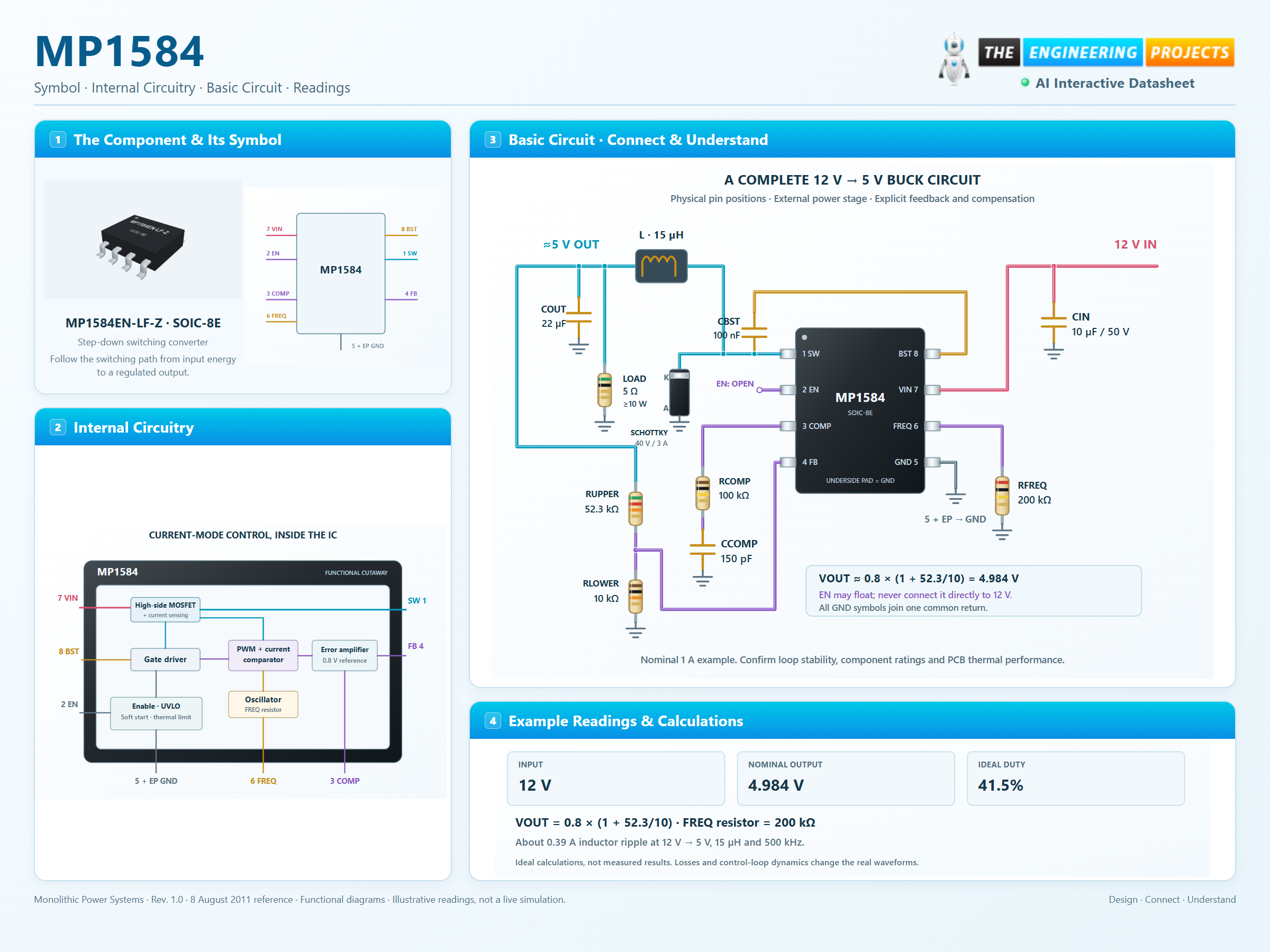
3 stages · Explore one step at a time
During the on interval, current flows from VIN through the MOSFET and inductor into the output.
During the off interval, the Schottky diode conducts from ground into SW, completing the inductor-current path.
FB senses the output divider. COMP and the FREQ resistor shape the response and nominal switching rate.
Physical SOIC-8E pin positions with the external power and control networks.
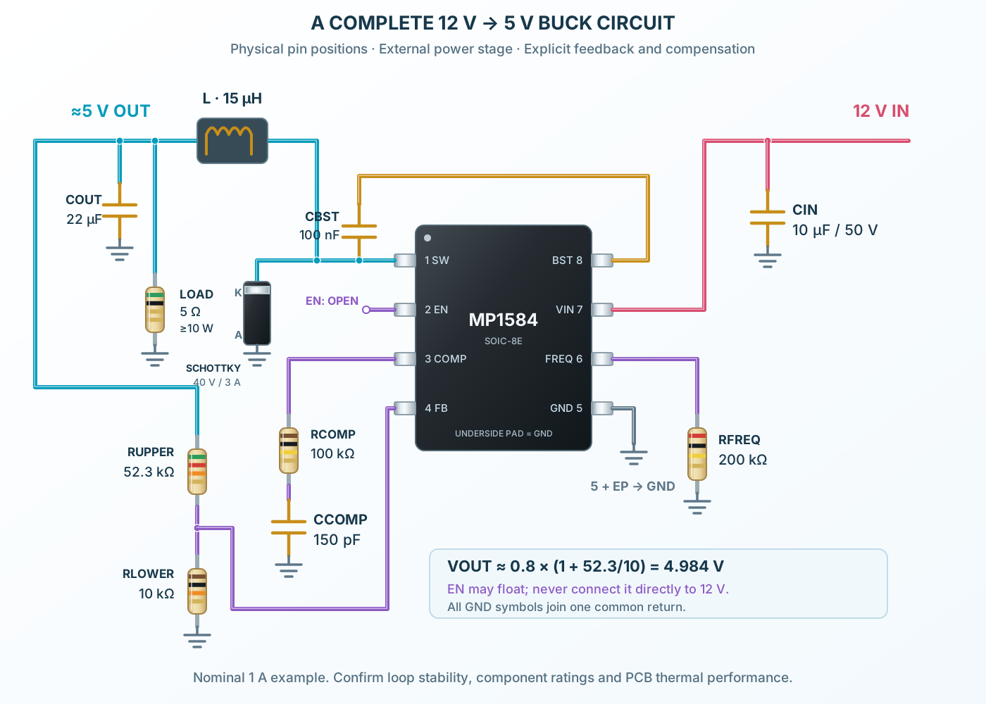
Follow the component values and pin connections
VIN takes the bypassed 12 V input; SW feeds the inductor and diode cathode.
Connect the output divider, FREQ resistor and COMP series RC.
Ground pin 5 and the underside exposed pad; keep the physical switching loop short.
A compact functional cutaway of the current-mode buck controller.
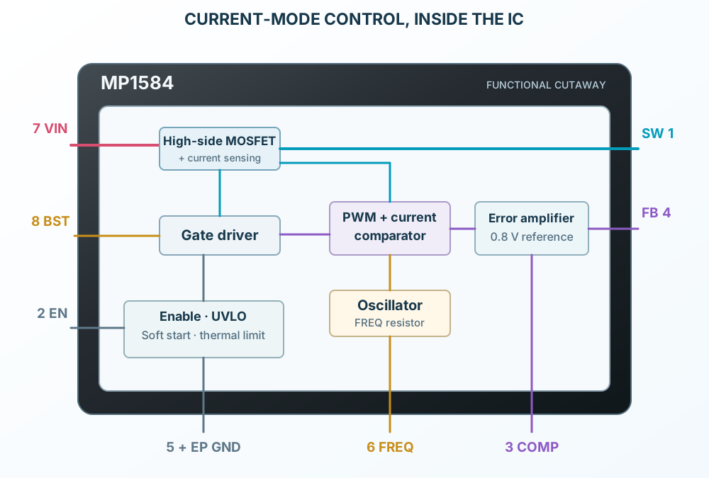
Select a stage to see its role and connections
The 0.8 V reference and error amplifier process the FB voltage.
A bootstrap-powered driver operates the integrated MOSFET.
Current limiting, UVLO, soft start and thermal control constrain the power stage.
Signal names, electrical functions and connection guidance
Scroll within the table to see all columns and rows.
| Pin | Signal | Type | Function & connection |
|---|---|---|---|
| SW | Switching power node | The internal high-side MOSFET drives this node. The inductor and external catch diode complete the buck power stage.Connection guidanceConnect the inductor to the output and the Schottky cathode to SW; its anode returns to ground. SW is a noisy switching node, not the regulated DC output. | |
| EN | Enable input | A high level enables operation; a low level disables it. An open pin also enables the device.Connection guidanceLeave open for the fixed 12 V example, or drive within the specified pin limits. Typical rising threshold 1.5 V. Do not tie EN directly to a 12 V input; its absolute maximum is 6 V. | |
| COMP | Loop compensation | Error-amplifier output used to shape the converter feedback loop.Connection guidanceFit the reviewed series RC network from COMP to ground. Compensation depends on the inductor, output capacitance, ESR and operating conditions. | |
| FB | Output-voltage feedback | The control loop compares the divided output to a nominal 0.8 V reference.Connection guidanceConnect the midpoint of the output-to-ground divider. Route away from SW and the high-current loop. | |
| GND | Ground and exposed pad | Return for control and power circuitry. The exposed underside pad also connects to ground.Connection guidanceJoin pin 5 and the exposed pad to a suitable ground plane. The footprint repeats electrical pad number 5 on the exposed pad; it does not invent a separate signal pin. | |
| FREQ | Frequency programming | A resistor from FREQ to ground sets the switching frequency.Connection guidanceUse 200 kΩ in the approximately 500 kHz example. The frequency setting is nominal; light-load pulse skipping changes the observed switching activity. | |
| VIN | Input supply | Supplies the internal control and high-side switching stage.Connection guidancePlace a low-ESR input bypass close to VIN and the power return. Operating input is 4.5–28 V; 30 V is an absolute stress limit, not a working target. | |
| BST | Floating bootstrap supply | Provides gate-drive supply above the SW node.Connection guidanceConnect 100 nF between BST and SW, with short traces. Observe the 6 V absolute BST-to-SW limit; this capacitor does not connect to ground. |
No pins match these filters. Try another signal name or reset the filters.
MP1584EN · limits and test conditions
Scroll within the table to see all columns and rows.
| Parameter | Value | Conditions / notes |
|---|---|---|
| Input supply | 4.5–28 V | Recommended operating range |
| Output adjustment | 0.8–25 V | Must remain below input with adequate headroom |
| Output-current class | 3 A | Limited by power components, temperature and layout |
| Operating junction | −20 to +125°C | Do not use shutdown temperature as an operating target |
| Ambient ordering range | −20 to +85°C | MP1584EN package reference |
| Package | SOIC-8E | Eight leads plus a grounded exposed pad |
| Lifecycle note | Not recommended for new designs | MPS identifies MP2338 as an alternative; it is not pin-compatible by assumption |
No specifications match. Try a parameter name or a unit.
Electrical table baseline is VIN = 12 V, VEN = 2.5 V, VCOMP = 1.4 V and TA = 25°C unless stated.
Separate nominal behavior from guaranteed limits
Scroll within the table to see all columns and rows.
| Parameter | Value | Conditions / notes |
|---|---|---|
| Feedback voltage | 0.776 / 0.800 / 0.824 V | Minimum / typical / maximum; 4.5 V < VIN < 28 V |
| High-side on resistance | 150 mΩ typical | BST − SW = 5 V |
| Current-limit threshold | 4.0 A minimum; 4.7 A typical | No maximum is stated here; not a 3 A output guarantee |
| UVLO rising threshold | 2.7 / 3.0 / 3.3 V | Internal threshold; operation still requires the specified input range |
| UVLO hysteresis | 0.35 V typical | Input undervoltage control |
| EN rising threshold | 1.35 / 1.50 / 1.65 V | EN hysteresis 0.30 V typical |
| No-load quiescent current | 100 µA typical; 125 µA maximum | FB = 0.9 V |
| Shutdown current | 12 µA typical; 20 µA maximum | EN = 0 V |
| Soft start | 1.5 ms | Design-guaranteed source value; FB from 0 to 0.8 V |
No specifications match. Try a parameter name or a unit.
Typical values do not establish worst-case performance.
The example follows the 5 V compensation row
Scroll within the table to see all columns and rows.
| Parameter | Value | Conditions / notes |
|---|---|---|
| Programmable frequency | 100 kHz–1.5 MHz | External resistor at FREQ |
| RFREQ relationship | RFREQ[kΩ] = 180000 / f[kHz]^1.1 | Approximate design equation |
| Example RFREQ | 200 kΩ | Approximately 485 kHz by the equation; nominal 500 kHz class |
| Example output inductor | 15 µH | Source table lists 15–22 µH for 5 V / 22 µF output |
| Example output capacitor | 22 µF low-ESR ceramic | Account for capacitance loss under DC bias |
| COMP series network | 100 kΩ and 150 pF to ground | Source 5 V compensation row |
| Extra COMP capacitor | Not fitted in this example | Evaluate separately for high-ESR output capacitors |
No specifications match. Try a parameter name or a unit.
Changing power-stage components can require a new loop-stability review.
Illustrative 1 A load · regulated bench input
Scroll within the table to see all columns and rows.
| Parameter | Value | Conditions / notes |
|---|---|---|
| Input / output | 12 V / 4.984 V nominal | Before reference, resistor and regulation errors |
| Feedback divider | 52.3 kΩ upper; 10 kΩ lower | Use 1% resistors; nominal divider current 80 µA |
| Bootstrap capacitor | 100 nF | Between BST8 and SW1 |
| Input bypass | 10 µF, 50 V ceramic | Place close to VIN7 and the power return |
| Catch diode | 40 V Schottky, at least 3 A class | Cathode at SW; anode at GND; check losses and surge ratings |
| Output inductor | 15 µH, ≥4 A saturation rating for normal operation | Check RMS current and fault behavior separately |
| Output capacitor | 22 µF, 10 V ceramic | Effective capacitance and ESR matter |
| Example load | 5 Ω, at least 10 W | About 1 A and 5 W; resistor will dissipate heat |
| EN connection | Open | Fixed 12 V input example; do not tie EN to VIN |
| Ideal inductor ripple | About 0.39 A peak-to-peak at 500 kHz | 12 V input, 5 V output, 15 µH; continuous-conduction approximation |
No specifications match. Try a parameter name or a unit.
This is an engineering starting circuit, not a claim of tested converter hardware.
Short power paths; quiet feedback
Scroll within the table to see all columns and rows.
| Parameter | Value | Conditions / notes |
|---|---|---|
| Hot loop | Input bypass → VIN / switch → catch diode → return | Keep the switching-current loop compact |
| SW copper | Short connection to inductor and diode | Keep clear of FB and compensation traces |
| Exposed pad | Connect to ground copper | Thermal vias and solder stencil need assembly-specific review |
| Bootstrap loop | BST capacitor close to BST and SW | Do not connect this capacitor to ground |
| Light-load headroom | VIN − VOUT greater than 3 V | Source guidance for refreshing the floating bootstrap supply |
| High duty ratio / low input | Review external bootstrap diode guidance | Source recommends it when VOUT/VIN >65% or VIN <5 V |
| Feedback pickup | Sense the regulated output after the inductor | Keep the divider and COMP components close to the IC |
No specifications match. Try a parameter name or a unit.
The fixed 12 V-to-5 V example provides generous bootstrap headroom.
Stress ratings are not normal operating conditions
Scroll within the table to see all columns and rows.
| Parameter | Value | Conditions / notes |
|---|---|---|
| Junction-to-ambient reference | 50°C/W | JESD51-7 four-layer test board |
| Junction-to-case reference | 10°C/W | Source package metric |
| Thermal shutdown | 150°C typical | 15°C typical hysteresis |
| Input absolute maximum | 30 V | Normal operation limited to 28 V |
| BST relative to SW | −0.3 to +6 V | Absolute stress limits |
| Other control pins | −0.3 to +6 V | Includes EN; do not connect directly to a high input rail |
| Absolute junction / storage | 150°C / −65 to +150°C | Stress / storage ratings |
No specifications match. Try a parameter name or a unit.
Actual temperature depends on switching losses, diode and inductor losses, copper and airflow.
MP1584EN-LF-Z · top-view numbering
Scroll within the table to see all columns and rows.
| Parameter | Value | Conditions / notes |
|---|---|---|
| Nominal molded body | 3.9 × 4.9 mm | SOIC-8E; 1.27 mm lead pitch |
| Body height | 1.30–1.70 mm | Manufacturer mechanical drawing |
| Lead span | 5.80–6.20 mm | Across the two banks |
| Exposed pad | 2.26–2.56 × 3.15–3.45 mm | Underside metal; electrically GND |
| Outer lands | 1.60 × 0.61 mm | 5.40 mm row centers; 1.27 mm pitch |
| Exposed land | 2.62 × 3.51 mm | Same electrical pad number 5 as the GND lead |
| Surface mounting only | SOIC-8E | No through-hole version is presented |
No specifications match. Try a parameter name or a unit.
The original footprint is a starting land pattern; review mask, stencil, vias and assembly clearances.
No matching rowsTry a pin name, parameter, unit or test condition, or reset the filters.
Understand compact MP1584-based supplies and their operating limits.
Manufacturer application guideTrace on/off current paths, feedback and the bootstrap supply.
Manufacturer application guideCheck ground-pad cooling, diode polarity and separation of SW from feedback.
Manufacturer application guideFind MP1584 in the Components Library to place its schematic symbol and connect its pins.
Reference page · circuit simulation model not yet availableOpen ProTech